Examples of Research and Development Interests of R. Jacob Baker, PhD, PE
Recent funding is
seen below.
In-kind, equipment, gifts, software, and non-contract/grant funding (such
as free integrated circuit fabrication support) is not listed below.
- Baker, R. J., (2023-2024) "Silicon Germanium (SiGe) Avalanche Photo Diode (APD) Chip," Department of Energy, Mission Support and Test
Services (MSTS), LLC, $120,000
- Baker, R. J., (2017-2023) "Tiled
Silicon Photomultiplier Array Read-Out Integrated Circuit," NASA, $29,999
(Phase I), $225,238 (Phase II), and $79,697 (Phase IIE)
- Goldman,
J., Menezes, J., and Baker, R. J., (2021-2022) "Monitored Compression
Therapy: Using Smart Technology to Optimize the Treatment of Lower
Extremity Swelling," UNLV Sports Research & Innovation
Initiative. Proof of Concept Grant Program, $50,000
- Baker, R. J.,
(2019-2021) "Dual-Mode, Extended Near-Infrared, Focal Plane
Arrays Fabricated with CMOS Compatible GeSiSn Alloy Materials,"
DARPA, $149,998
- Baker, R. J., (2018-2020) "Geiger
Mode SiGe Receiver for Long-Range Optical Communications," NASA,
$99,996
- Baker, R. J., (2019) "Improved Quantum
Efficiency Photo-Detector," Navy, $29,999
- Baker, R. J., (2018-2019) "Tiled
Silicon Photomultiplier Array Read-Out Integrated Circuit - Phase I,"
NASA, $29,999
- Baker, R. J., (2017-2019) "Quantum Cryptography Detector
Chip," Defense MicroElectronics Activity (DMEA), $266,029
- Baker, R. J., (2017-2019) “Advanced
Printed Circuit Board Design Methods for Compact Optical Transceiver,”
U.S. Army/DOD, $299,605
For specific
details of the work listed below, in addition to the associated links,
see the resulting patents,
talks/papers, and dissertations/theses.
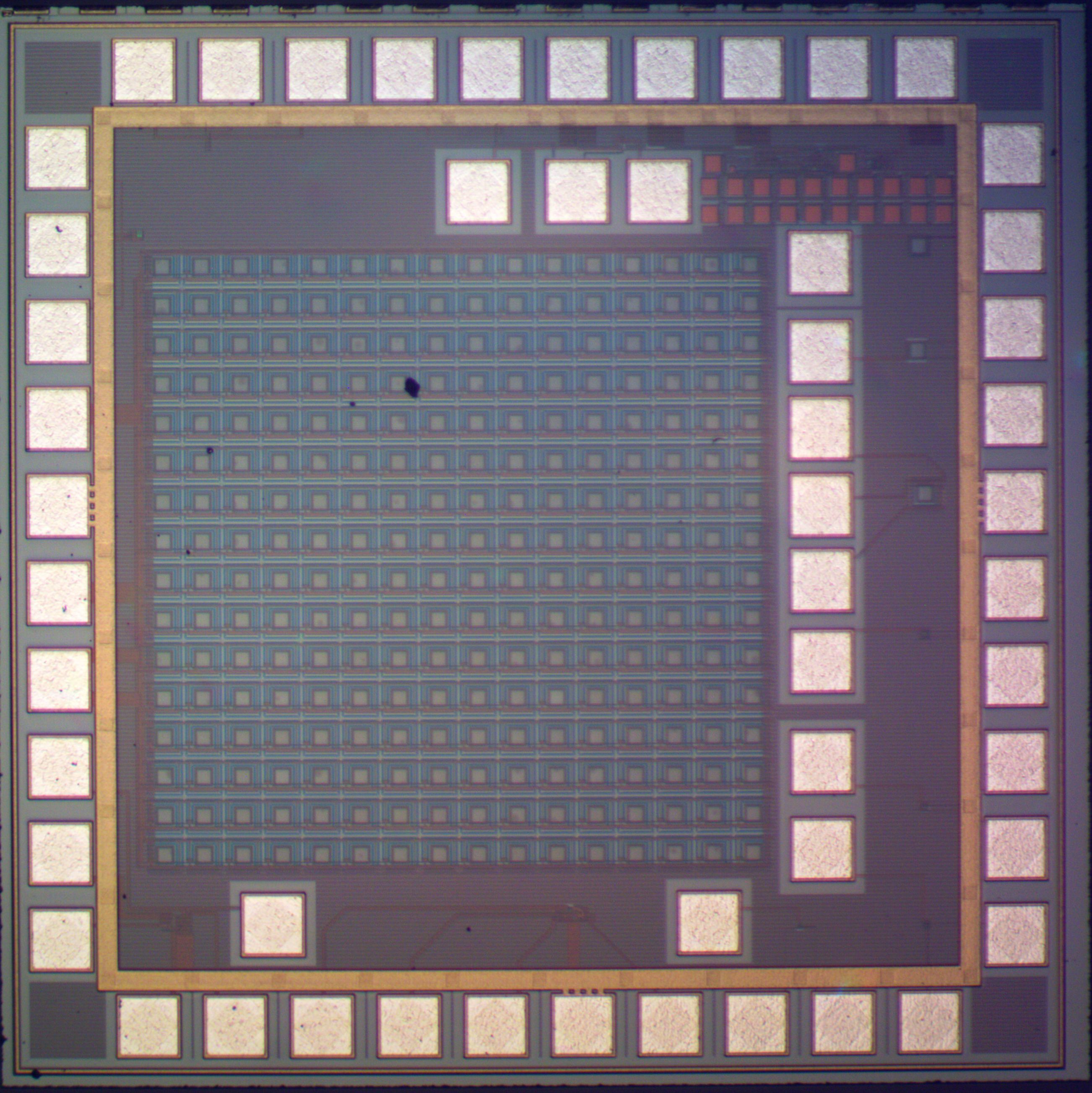
- A few chips from our group: Multi-Channel ROIC, Wide-Swing FTD, Photon Counting, Solar Sailer, Voyager, TDC_chip, and Frank Sinatra
- Information on a SiGe test chip (image)
containing test structures including SiGe APDs, Silicon Photomultipliers,
TIAs, and low-power DSM is found here
- Test results comparing SiGe and Si
APDs are found here
- Chip packaging and bonding to printed
circuit boards, information
on how we package chips at UNLV for Dr. Baker's students
- Design of integrated circuit
electronics and optoelectronics for optical transceivers used in
LIDARs/LADARs, (Vorpal Research Systems, 2017-2019)
- Development of range finders using
LEDs and lasers in compact optical transcievers, (Attollo Engineering,
2016-2019)
- Circuit design for the control, use,
and storage of renewable energy using thermoelectric
generators
- Design of electrical/biological
circuits and systems using electrowetting on
dielectric for automating and controlling biological experiments
- Design and fabrication of
single-photon avalanche diodes (SPADs) and silicon photomultiplier (SiPM)
using Geiger
mode APDs, (Freedom Photonics, 2014-present)
- The design of a transient digitizer
integrated circuit for scientific diagnostic instrumentation, (National
Security Technologies, 2014-2015)
- Design of CMOS imagers, memory,
interfaces, and packaging for commercial CMOS image sensor products, (OmniVision,
2013-2015)
- Design of transimpedance amplifiers (TIAs) in CMOS for
LIDAR/LADAR pulse processing, (Areté Associates, 2013)
- Analog-to-digital converters and
signal processing for capacitive touch displays and pads, (Cirque,
2013)
- Low temperature CMOS circuit design
for infrared focal plane array readouts, (Lockheed Martin Santa Barbara
Focalplane, 2012)
- Laid out a test chip using TowerJazz’s
CA18QD process to characterize APDs and LNAs for
LADAR/LIDAR applications, (USAF, 2012)
- Designed CMOS silicon avalanche
photodetectors (APDs) and laid out a test chip, in On’s
C5 process, to characterize the APDs for use in high-speed imaging and
LADAR/LIDAR applications, (FLIR, 2011-2012)
- Worked on the design of readout integrated
circuits (ROICs) for use with various focal plane arrays (FPAs), (Aerius
Photonics, 2010-2011)
- Design using, and fabrication
of, Memristors to implement reconfigurable
analog electronics with CMOS technology, (AFRL, 2011)
- Designed a Flash LIDAR/LADAR ROIC unit
cell, (Areté Associates, 2010)
- CAD tool development, use and
educational tutorials, see CMOSedu.com
- Worked with Sun, and then Oracle, on
the design and fabrication of memory modules (DRAM, Flash, PCRAM, combinations of various technologies) using proximity
communication, wide IOs, and 3D packaging, (Oracle, Inc.,
2009-2010)
- NMOS voltage and current references,
charge pumps, voltage regulators, and power up/down circuits for
phase-change memory chips, (Contour Semiconductor, Inc., 2009-2010)
- Using the K-Delta-1-Sigma
modulator for Gsample/s data converter design
- Sensing schemes for
new memory fabrication technologies
- Circuit design, fabrication
(chemical-mechanical polishing [CMP] and Bosch etch), and 3D packaging (e.g., flip-chip for solder ball connections to adjacent die or to a carrier or package)
applications of Thru-Silicon
Vias (TSVs), (DARPA, 2000-2011)
- Low-overhead voltage regulators for
DRAM memory chips
- High-speed digital timing circuits
including input buffers, delay-locked loops and comparators
- Chemical and biological sensor
fabrication using nanostructures with CMOS processes, (2007-2009)
- Design of delta-sigma
imager sensors
- Noise-shaping analog-to-digital
conversion
- Layout techniques to improve circuit
performance
- Computer Aided Design (CAD) software
tool development for integrated circuit design and fabrication, (Electric VLSI
and LASI)
- Designed and tested delta-sigma
sensing circuits for drastically improving sensing in Flash memory and
process technology development at the 35 nm node, (Micron
Technology, Inc., 2005-2008)
- MEMS capacitive sensor fabrication and
readout integrated circuit design, (EPA, 2004-2006)
- ChemFET fabrication and Ion Mobility Spectrometers (IMSs) for sensing contaminants, (EPA, 2003-2004)
- Design of array/peripheral circuitry including
pipelined ADCs for CMOS imager chips, (Photobit/Micron, 2001-2003)
- Designed Schottky diodes in a standard
CMOS process for use in radio-frequency applications, (AFRL,
2001-2006)
- A high-speed low-power 10-bit DAC,
(design done at the request of a VC firm, 1999)
- 64 MHz DAC for power line
communications, (ITRAN Communications, 1999)
- High-speed clocked comparator for
spread spectrum communications (ITRAN Communications, 1999)
- Pre-amplifier
with clipped output (ITRAN Communications, 1999)
- Power op-amp for
driving 30 ohm equivalent load (ITRAN Communications, 1999)
- An R-2R type 10-bit
(and an 8-bit version) DAC in 0.18 um CMOS (Amkor Wafer Fabrication
Services, 1999)
- Fabrication and design of a PLL for an
embedded DRAM
chip (Micron Technology Inc., 1999)
- Designs ranging from pipeline ADCs
to switching power supplies in memory chips, (Micron Technology,
Inc., 1998-2008)
- Low-power CMOS crystal oscillator (Tower
RDT ASIC center, Israel, 1998)
- High sensitivity comparator with
0.5 mV hysteresis (Tower RDT ASIC center, Israel, 1998)
- Pixel clock generator
from a PCI clock for a GPU (Rendition, Santa Clara, 1998).
- CMOS PLL design in
submicron CMOS (Amkor Wafer Fabrication Services, 1998)
- Design of double-data rate (DDR)
circuits to transition SDRAM to DDR-SDRAM (Micron Technology, Inc.,
1998-2000)
- High-speed (>500 Mbits/s), low-skew fully-differential digital
receiver/transmitter design
(Micron Technology, Inc., 1998)
- Test
DLL for data rates up to 500 Mbits/s for
high-speed transfer of data (ultimately DDR), (Micron Technology,
1998)
- CMOS precision voltage reference
without substrate injection (Micron Technology, 1997)
- Power up/down
circuit using a bandgap and an MOS voltage reference for
enabling/disabling charging of a battery or super capacitor (Tower
Semiconductor, Israel, 1997)
- Design of USB interfaces using 0.6 um
CMOS technology for consumer products (Tower Semiconductor, Israel, 1997)
- 10 MHz 8-bit D/A converter
that can drive low resistance load used in a modem processor (Tower
Semiconductor, Israel, 1997)
- High-speed receiver for a
modem processor (Tower Semiconductor, Israel, 1997)
- NTSC video circuit design (sync
separator, automatic gain control, etc.) in NMOS, (Micron Technology,
Inc., 1994-1996)
- NMOS-only PLL for a field emitting
display to generate a pixel clock from NTSC horizontal sync, (Micron
Technology, Inc., 1995)
- Integrated circuit fabrication of
field-emitting displays and peripheral video circuits, (Micron Technology,
Inc., 1994-1996)
- Designed the switched-capacitor pixel
driver for a field-emitting display using 5 um NMOS, (Micron
Technology, Inc., 1994)
- 2 kV pulse generator to drive Helmholz coils, (Lawrence Berkeley Labs,
1993-1994)
- Design of time-domain impulse radar
circuits for detection and sensing, (LLNL, 1993)
- Micro-channel plate image intensifiers (MCP) drivers for
high-speed photography, (E.G.& G. and LLNL, 1986-1993)
- Designed all sorts of discriminators and
triggering circuits for nuclear diagnostic instrumentation, (E.G.&
G. and LLNL, 1986-1993)
- HV sweep circuits for streak cameras
and drivers for Pockel’s cells used in femto- and pico-second
electro-optic instrumentation, (E.G.& G. and LLNL, 1986-1993)
- Avalanche and MOSFET transistor pulse
generators for use in high-speed instrumentation, (E.G.& G. and
LLNL, 1986-1993)
- SRAM memory design for storing CCD
data operating at up to 100 MHz, (E.G.& G. and LLNL, 1986-1993)
- Battery charger and back-up system for
a mobile SRAM memory system, (E.G.& G. and LLNL, 1989)
- Hybrid (on alumina) integrated circuit
vertical amplifier design for E.G.& G.’s 10 GHz TWT using HBTs
supplied by TI, (E.G.& G. and LLNL, 1989-1991)
- Design of bit and frame-syncs (SerDes)
for high-speed (90, 180, and 720 Mb/s) communications using board-level
ECL, (E.G.& G. and LLNL, 1988-1991)
- Camera design using E.G.& G. Reticon CCDs, (E.G.& G. and LLNL,
1988-1991)
- Fiber-optic transmitter and receiver
design for 2 km serial links MM and SM fibers at 800 and 1300 nm
wavelengths, (E.G.& G. and LLNL, 1987-1991)
- Equalizer design, DC restore using
envelope tracking, system design for high frequency analog and digital
signal transmission (electrical and optical), (E.G.& G. and LLNL,
1987-1991)
- Writing software (link) to simulate the behavior of short-channel semiconductor devices, (UNLV, 1987-1988)
- Digital-to-analog calibration system
for calibrating ADCs in CCD imaging chips, (E.G.& G. and LLNL,
1986-1987)
- Design of linear and switching power
supplies for more than a dozen diagnostic instruments, (E.G.& G.
and LLNL)
- Design of high-voltage pulse and ramp
generators using planar triodes and krytrons, (E.G.& G. and LLNL,
1986-1987)
- Hand-held battery-operated tunnel
diode pulse generator for checking compensation of oscilloscopes at the
Nevada Test Site, (E.G.& G.
and LLNL, 1985-1986)
- Primary and secondary power system
design, installation and troubleshooting electric motors on mining
equipment, (Reynolds Electrical Engineering Company [REECo], 1985)
Return