Below are the
photos and some other information on the test DLL designed for Micron's Double
Data Rate DRAM. The DLL uses a symmetrical delay line for tight locking on both
the rising and falling edges. The design shown here worked beyond 250MHz (500 Mbits/s for DDR DRAM since we clock data in on both the
rising and falling edges). This design was tested during April of 1998.
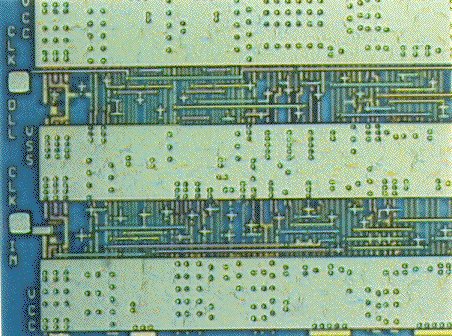
Photo of the phase detector
implemented in a 0.25 um process. This test section was implemented in the
scribe of a development wafer.
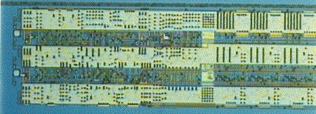
Below is a zoomed out view showing
the phase detector, delay element and control logic. The test circuit contained
48 delay elements and measured 95um high and 1775 um long.
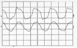
Input (bottom) and output of the
DLL at 200 MHz are shown below (2ns/div). Note how the input looks sinusoidal.
We used a femto probe to make the input/output
measurements where the input was applied through a standard microprobe from a
twin lead clip (not a good high frequency connection!) through a BNC tee where
the other end of the cable was terminated using the 50 ohm input of an o-scope
(and used for a solid scope trigger). A computer program we had for the scope
we were using said that one sigma for a jitter measurement was 79 ps while the range of jitter over 7,000 sweeps was under
+/- 200 ps.