Modem
Receiver Circuit
Designed and
laid out in 1997 by Jake Baker for Tower Semiconductor
The
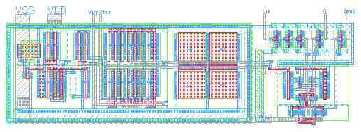
cell pictured above is a Receiver circuit for use in a high speed modem.
Design
Specifications:
- Stage
1
- Differential
Amplifier with linear range of 0.7V - VDD-0.7V
- Offset
voltage of +/- 1.5mV
- VDD=5V
+/- 10%
- DC
Current < 0.3mA
- Amplification
7-15 (typically 10)
- Frequency
response up to 1MHz
- PSRR
> 70dB
- Input
current < 1uA
- Stage
2
- RC
type passive LPF
- Linear
Range of 0V - VDD
- RC
factor > 3uS
- Noise
from VDD or GND is halved at the LPF output
- Stage
3
- S/H
Circuit
- Input
voltage range 1V to VDD - 1V
- Sampling
frequency 0.25uS typically
- Stage
4
- Comparator
- Full
Swing output
- Response
time is 10nS
- VDD
= 5V +/- 10%
- DC
current < 0.3mA
The cell was designed using a 0.6 micron, double metal, single
poly process.