Silicon
APD Test Chip using ON’s C5 Process
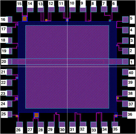
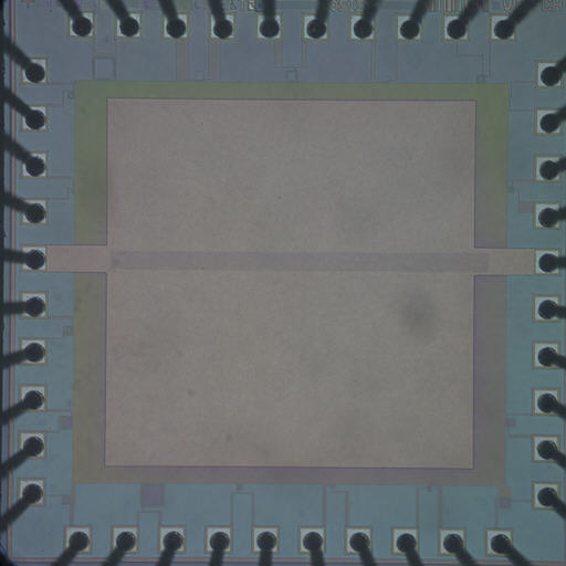
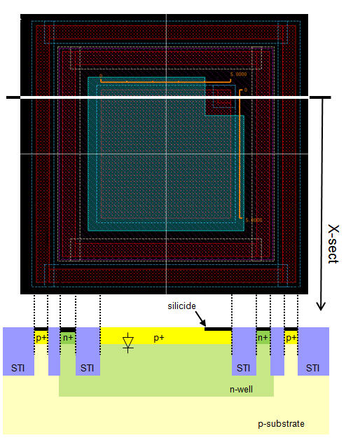
Shown below are images
of a chip laid out by Jake
Baker in 2011 for
measuring the characteristics of CMOS Avalanche PhotoDetectors
(APDs) fabricated in ON’s
C5
process through MOSIS.
It’s important to
ensure neither metal nor silicide (not used in the C5 process) cover
the active
area. It’s also important, for good behavior, to avoid corners or sharp
changes
in the geometry in the pn
junction that is breaking
down (see cross-sectional image below). Click images to enlarge.
Montierth,
D., Strand, T., Leatham,
J., Linder, L., and Baker, R. J., "Performance
and Characteristics of Silicon Avalanche Photodetectors in
the C5 Process,” Proceedings
of the 55th Midwest
Symposium on Circuits and Systems,
August 5-8, 2012. (slides)
Last
Updated (added paper and slides link) Tuesday, August 6, 2012
Updated
Wednesday, December 14, 2011