Using
TSVs (aka Thru-Wafer Vias) to Implement
On-Chip Inductors
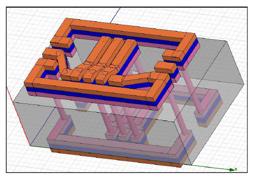
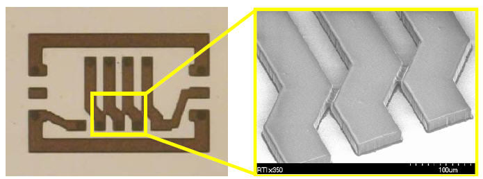
Above
(left) showing the HFSS simulation of an inductor implemented using
Thru-Silicon Vias (TSVs) and (right) an inductor fabricated in the Idaho
Microfabrication lab
using
TSVs.
The
development of TSV technology at Boise State was supported by DARPA and
started
in 2000. While much of our work focused on using this technology for 3D
packaging (e.g., flip-chip for solder ball connections to adjacent die or to a carrier or package),
the implementation of large-value inductors represents a novel use of
the TSV.