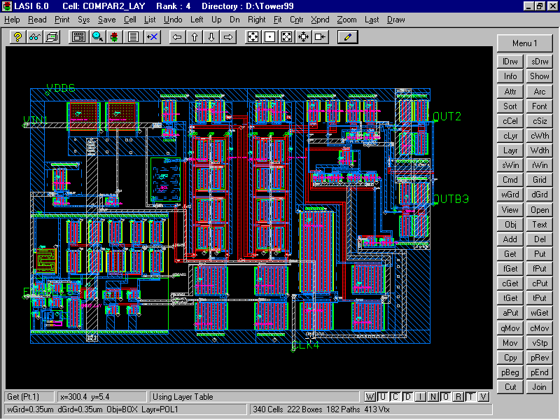
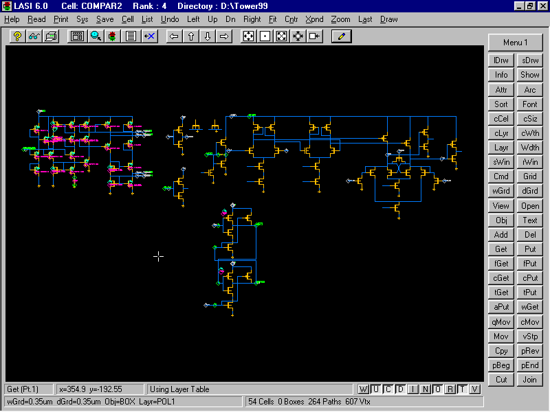
Below are the
schematic and layout of a comparator designed and laid out by Jake Baker in 1999 for a power
line communications chip designed by ITRAN communications. The process used is
Tower Semiconductors 0.35 um process. Since it is a single poly process it is
challenging to design the comparator with some sort of offset storage. Since
the input to the comparator is single ended, and AC coupled, and the comparator
was to be operated as a zero-crossing detector clocked at 64 MHz, we amplified
the single-ended input signal so that it was large compared to the offset
voltage of the second stage diff-amp. The inputs to the second stage diff-amp
are the input and output of the push-pull amplifier on the input of the
comparator. The comparator also has the feature that it can be disabled to
force it into a low-power "sleep" mode.