Phase-Locked
Loop for embedded DRAM/graphics chip
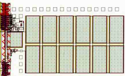
Below is the layout of a PLL designed by Jake Baker for use in an
embedded DRAM/graphics chip during the spring of 1999.
Below is the layout of a PLL designed by Jake Baker for use in an
embedded DRAM/graphics chip during the spring of 1999.