Wide-Swing FTD and a 4
channel Sample & hold array
Contributors
Angsuman Roy (angsumanroy@gmail.com)
Chip Orgainization
This chip is
designed using ON’s 500nm process in 2020. It comprises the following circuits:
1)
A 64 stage wide-swing fast transient digitizer
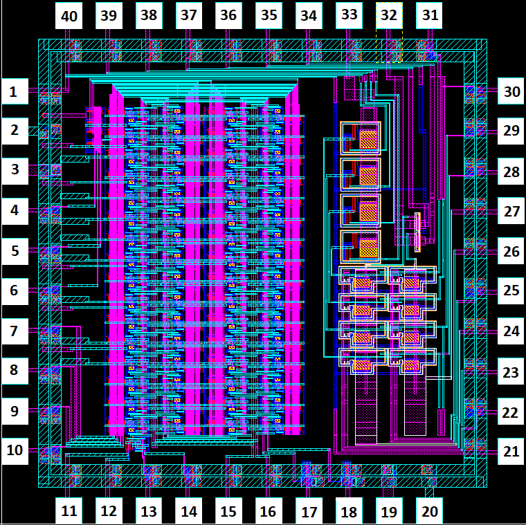
Figure 1.
Complete chip layout
Wide Swing FTD
|
Pin Number |
Signals |
|
4 |
Enable |
|
5 |
F |
|
6 |
E |
|
7 |
D |
|
8 |
C |
|
9 |
B |
|
10 |
A |
|
11 |
Rbias |
|
12 |
Vinvco |
|
13 |
Reset |
|
14 |
Trigger |
|
15 |
In |
|
16 |
Out |
|
17 |
Low_out |
|
18 |
High_out |
Sample and
hold array
|
Pin Number |
Signals |
|
22 |
S1 |
|
24 |
H1 |
|
25 |
S2 |
|
27 |
H2 |
|
28 |
Read_4 |
|
29 |
Read_3 |
|
30 |
Read_2 |
|
31 |
Read_1 |
|
34 |
Source_2 |
|
36 |
Source_1 |
|
37 |
PD1 |
|
38 |
PD2 |
|
39 |
PD3 |
|
40 |
PD4 |
Power Supply
|
Pin Number |
Signals |
|
3,19 |
VDDW, VDDS |
|
2,20 |
GNDW,GNDS |
|
21 |
GNDE(S/H) |
|
23 |
VDD_1(S/H) |
|
26 |
VDD_2(S/H) |
|
32 |
VDD_Buffer(S/H) |
|
33 |
VDD_TIA(S/H) |
|
35 |
Gnd_2(S/H) |
|
1 |
Gnd_1(S/H) |