Packaging
Information for Dr. Baker's Research Group
The following information is intended to inform members of Dr. Baker’s research team how to package a chip/die for testing. Specifically, information on common die sizes, how to layout printed circuit boards (PCBs), fabricating PCBs and choosing the laminate and surface finish, example PCBs, and using the wire bonder, as well as purchasing packages, wire bonding consumables, and other consumables such as surface mount components.
- Common Die Sizes
- Package Information
Commonly Used Packages
SOIC-24, SOIC-28, SSOP-16, SSOP-28, LCC44, LCC64, Cerquad-44
SOIC packages are preferred for easy soldering, but they have more parasitics. SSOP packages have low parasitics and are easy to solder, so they are preferred for high speed applications. LCC44 and LCC64 packages are used if we need to bond out every single pad for a chip, but they are difficult to solder. Cerquad-44 packages (which we have some sockets for) are older, but they are easy to solder with high density.
Information on package parasitics:
Electrical Performance of Packages
Determining the Effects of Package Parasitics
Performance Characteristics of Packages
- Purchasing Packages
Evergreen Semiconductor
For Evergreen Semiconductor, you must send a request email then call them to provide credit card information, for which they charge $5. They sell in surplus, so you must inquire as to what they have in stock. If they do not have the exact package you are interested in, they may have a similar package (say a SSOP-24 instead of a SSOP-28), so you can see if your design can accommodate for a similar package. This is why we always buy the package BEFORE designing the PCB.
Spectrum Semiconductor
For Spectrum Semiconductor, use their online form and wait for them to contact you.
SSOP packages are kind of rare because most companies do prototyping in larger packages then might use a cheap plastic molded SSOP package for production, but we need high performance SSOP packages, so you usually have to request them specifically.
Amkor Technology
Kyocera
o Ceramic Packages
NTK Technologies
Creating PCBs
FreePCB Tutorial
o Design Tutorial
Diptrace Tutorial
Altium Tutorial
Eagle Tutorial
Use calipers to measure packages when creating a custom package footprint in any PCB software.
- PCB Fabrication Information
We've used HASL, OSP, Silver, ENIG, and ENEPIG.
We use HASL for low cost boards for student projects, but then we moved onto OSP because it only adds a small cost and it makes the smoothest surface finish for easy surface mount soldering. It also makes soldering easier because it has flux in the coating. But the disadvantage is the PCBs have to be stored well and the boards should only be handled by edges and should be stacked carefully with paper sheets in between. This is because the OSP coating is very thin. Also the OSP coating degrades after about a year so the boards should be used as soon as possible.
We tried Immersion Silver too because it provides a smooth surface finish and is longer lasting than OSP but costs more too. We don't use silver anymore because it tarnishes easily.
We use ENIG for high quality boards that don't require any chip on board (COB). ENIG is similar to OSP in terms of surface quality but is much more durable and lasts forever. ENEPIG is used for wirebonding directly to the PCB (COB). This is because the gold layer is thicker than ENIG (actually table says ENIG not good for gold wire bonding!). It is also more convenient than the traditional soft-gold coating because that requires electrolytic immersion which changes the PCB design considerably because all the traces have to be electrically connected and then later need to be cut back to the original traces. This is expensive and impractical for us.
To do ENEPIG coating we order OSP boards. Then strip the OSP coating with acetone. We do this instead of ordering bare copper boards because the OSP protects the boards in transit and also we tend to panelize multiple designs onto one board to save money. Non-wirebonded boards are already in the OSP finish and ready to solder. Boards that will be COB are then stripped with a few steps of acetone wash followed by deionized water.
Then they are shipped to Superior Processing, where they apply the ENEPIG coating and ship them back to us.
Information on Surface Finishes
PCB Surface Finishes – Advantages and Disadvantages
PCB Surface Finishes Comparison: HASL, OSP, & ENIG
ENEPIG PCB Surface Finish
Comparison
of Final Finish Performance
Where to Get
Boards FabricatedWe fabricate our PCBs through Gold Phoenix because they allow the ordering of a full 10 in. by 15.5 in. panel (which allows us to order a single panel consisting of multiple PCB layouts) with a wide variety of substrates and options including Rogers 4350 (for high frequency circuits) and FR-4 (for standard boards) laminates.
Cost:
o $180 for a HASL FR-4 board
o $440 for an OSP Rogers 4350 board
Price increases with more options, but we don't go past OSP finishes for the Rogers boards because we'll generally do an extra ENEPIG step for COB boards which tend to be high speed
- Example PCB layouts
o Footprints used
§ Custom footprint for Relay
§ Custom footprint for DCJack
§ RAD-248 for capacitors (C1, C2, C3, C4)
§ TO-220 for regulators (5VReg, 33VReg)
§ TO-92 for transistor (Tran)
§ DO-41 for diode (D1)
§ 8x2HDR-100 for headers (RFID)
§ 28DIP300 for Atmega328P socket (328P)
o Bottom Copper and Top Copper are both connected to “GND” net
o Only two traces were implemented on the bottom copper (red traces)
PCB Layout Fabricated PCB
PCB Layout Fabricated PCB
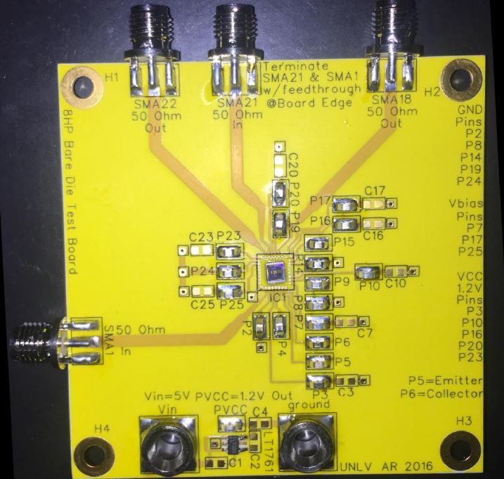
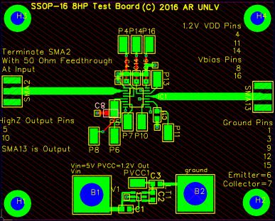
Above is an example of chip-on-board (COB) in which the chip/die is bonded directly to the printed circuit board (PCB).
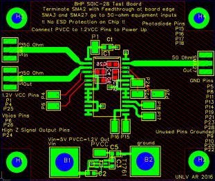
8HP SOIC-28 Test Board (FreePCB)
PCB Layout Fabricated PCB
Above is an example of bonding a chip to a package (SOIC-28) which is surface mount soldered to the PCB.
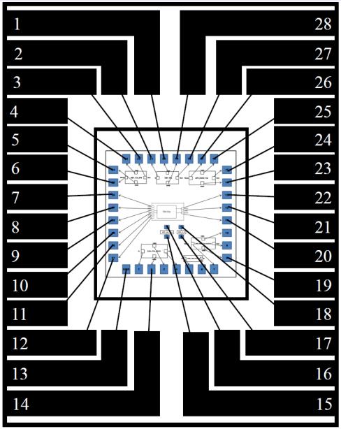
Above is the bonding diagram for bonding the chip/die to the SOIC-28 package.
Both the 8HP Bare Die and 8HP SOIC-28 PCBs were fabricated on Rogers RO4350B laminate, a low loss substrate made from a ceramic-hydrocarbon composite. Both the PCBs incorporate multiple features to facilitate testing. A local 1.2V LDO is used to create a high quality 1.2V supply for the on-chip TIAs. The high-speed inputs are coupled to the chip through 50-ohm SMA connectors and microstrips. The TIA outputs that can drive 50-ohm are also coupled through SMA connectors and microstrips. High-impedance, high-speed outputs from the CMOS TIAs are connected to test points as close to the package pins. A local ground point is located next to each high-speed pin so that an active probe can be easily connected. Finally, DC test points for I-V curves were placed further away as placement is not critical. See Consumables Purchased at Digi-Key below for links to SMA connectors, microstrip calculators, and test points.
Panelized Board – Rogers RO4350B Laminate (Sent in for Fabrication)
The picture above shows the panelized board that was sent in for fabrication on Rogers RO4350B Laminate. The panelized board consists of multiple copies of the 8HP Bare Die and 8HP SOIC-28 layouts as well as a third layout.
- Consumables Purchased at Digi-Key
BNC Connectors (Used for Random Projects)
Surface Mount Adapters (SMAs) (for microstrip)
o For microstrip we have to order a 31 mil thick (1/32nd inch) PCB because otherwise the microstrip has to be too fat. These SMAs only work on a 31 mil thick PCB.
Microstrip Calculator
o Use dielectric constant of 4.3 for FR-4 and 3.6 for Rogers boards
More Advanced Microstrip Calculator
Miniature Surface Mount (SM) Test Points for High-Density DC Tests, I-V Curves, High-Speed High-Impedance Pins
SM Resistors
o 10 – 97.6 ohm
o 100 – 976 ohm
o 1k - 9.76k ohm
o 10k – 97.6k ohm
o 100k – 976k ohm
o ...
o 10 – 910 ohm
o 1k – 91k ohm
o 100k – 10M ohm
SM Capacitors
o General Purpose
§ 1p – 10u farad
§ 10p – 0.22u farad
o RF, Microwave, High frequency
§ 0.2p – 30u farad
o High Voltage
§ 33p – 0.1u farad
o If we don’t have an exact resistor/capacitor value, use a value close to it.
Headers
- Using UNLV's Wire Bonder - Manual
§ Epoxy
§ Wire (gold)
o Quote for Epoxy and Wire
§ Wedges (Info in manual)
§ Bonding Diagrams
§ More Bonding Diagrams
Return


