Power
Up / Power Down Circuit
Using an MOS voltage reference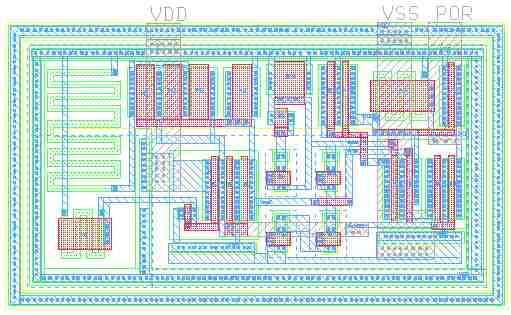
Using a bandgap
voltage reference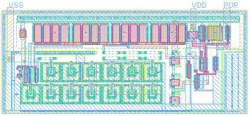
Designed and
laid out in 1997 by Jake Baker for Tower Semiconductor
The cells pictured above are
temperature insensitive Power Up/Power Down circuits.
Design Specifications:
- The inputs to the cell are only VDD and VSS
- The output is less than 0.7V if 0.7V < VDD < 4.1V
+/- 0.25V and is more than VDD-0.2V if VDD > 4.1V +/- 0.25V
- A small hysteresis (100-200mV) is included in the cell
The cells were
designed using a 0.6 micron, double metal, single poly process.