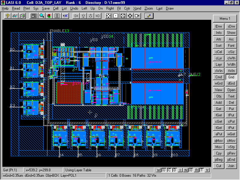
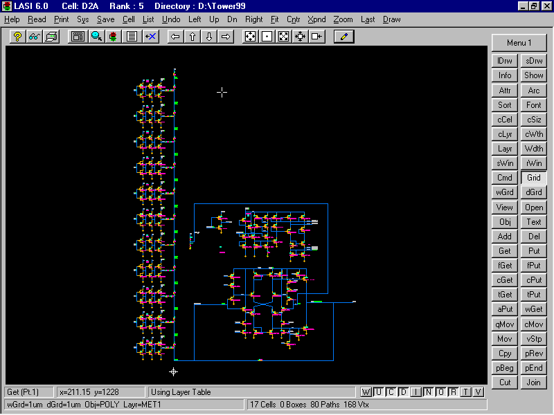
Below are the
schematic and layout of an 11-bit DAC (7-bits monotonic) designed and laid out
by Jake Baker in 1999 for a
power line communications chip designed by ITRAN communications. The process
used is Tower Semiconductors 0.35 um process. The chip uses the power op-amp
discussed here.
This DAC uses a novel R-2R architecture that allows the op-amp inputs to remain
at VDD/2 while allowing the output of the DAC to reach from ground to VDD.