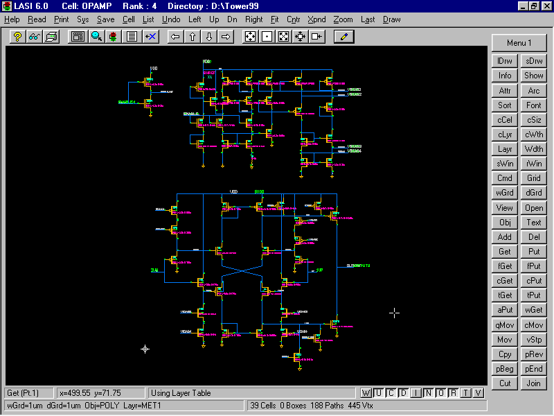
Below is a
schematic of a op-amp designed by Jake
Baker for a power line spread spectrum communications chip designed by
ITRAN communications. The process used is Tower Semiconductors 0.35 um process.
This op-amp is used to drive powerline and filters
with an effective input resistance of 30 ohms. It has the feature that it can
be put into a disabled mode so that it doesn't draw any significant amount of
current. Some interesting features of this design include the use of small
current sources and sinks to lower the quiescent current in the output stage.
This (small bias current in the output stages relative to the diff-amp bias current
and device sizes) causes the stability of the op-amp to become marginal under
certain load conditions. The pole associated with the output stage is
comparable, and under some situations has a value less, than the pole
associated with the output of the first stage. It was decided that this was OK
to minimize quiescent current draw while at the same time having a circuit that
can drive 30 ohms within 150 mV of the ground and 3.3V supplies (drive 100 mA
into the load). Another problem with this topology is that since current source
loads are used on both the top and bottom of the diff-pair the output stage is
not guaranteed to operate