SiGe APD and Various Structures Test Chip
Gonzalo Arteaga (arteag1@unlv.nevada.edu
R. Jacob Baker (rjacobbaker@gmail.com)
Tyler Ferreira (ferret1@unlv.nevada.edu
Dane Gentry (gentryd2@unlv.nevada.edu
James Mellott (
Eric Monahan (
Sachin P. Namboodiri (puruss1@unlv.nevada.edu
Angsuman Roy (angsumanroy@gmail.com
Raheel Sadiq (sadiqr@unlv.nevada.edu
Shada Sharif (sharifs@unlv.nevada.edu
Vikas Vinayaka (vinayaka@unlv.nevada.edu
This
test chip was fabricated using the ams 0.35um SiGe (S35) process and consists of the following circuitry:
·
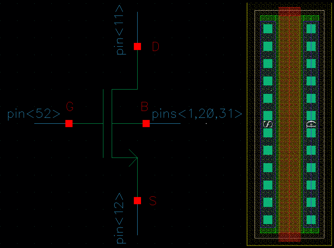
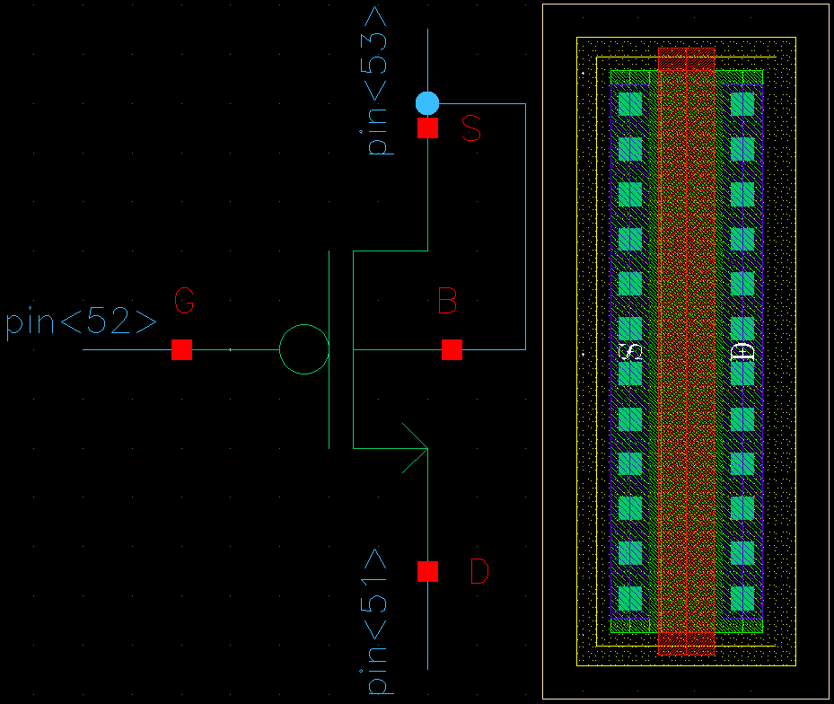
10u/1u NMOS and PMOS
·
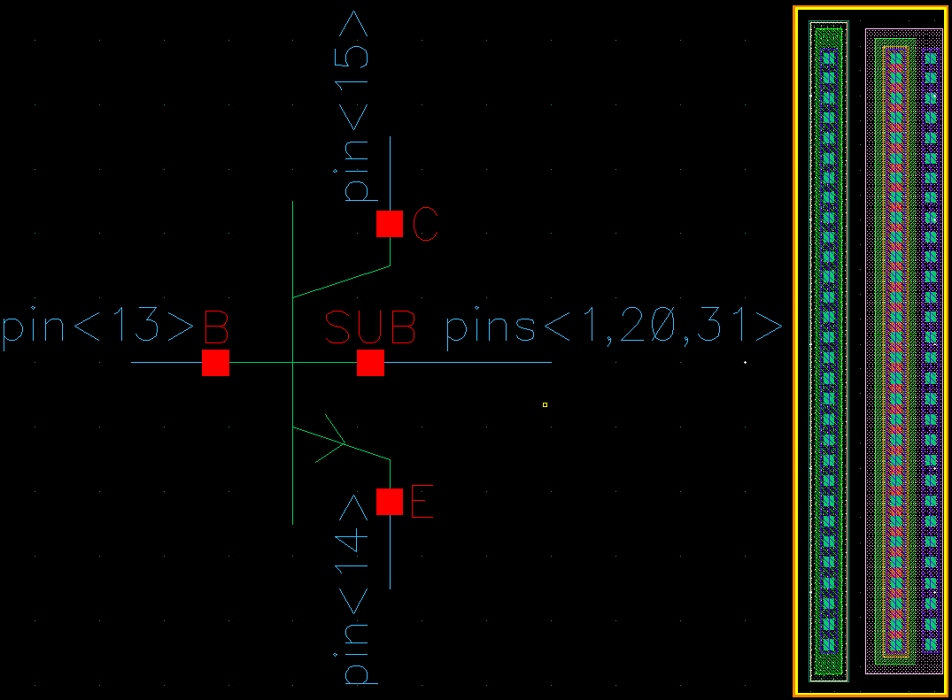
24u Area NPN BJT
(Bipolar Junction Transistor)
·
Single APD’s (Avalanche
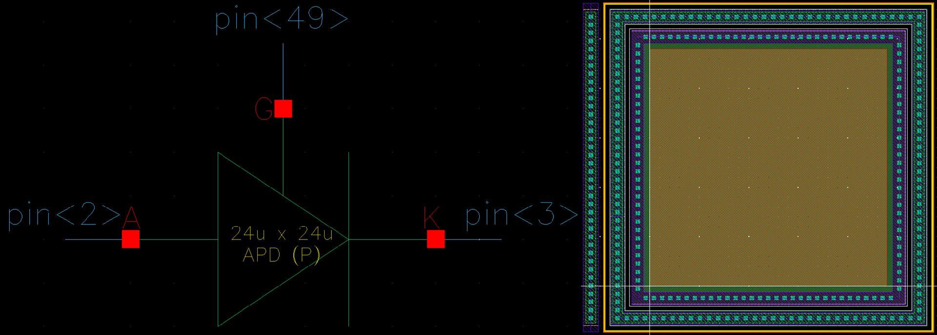
Photo Diode) with partial guard rings of the following sizes: 24u x 24u, 5u x
5u, 0.4u x 0.8u
·
Single APD’s with full
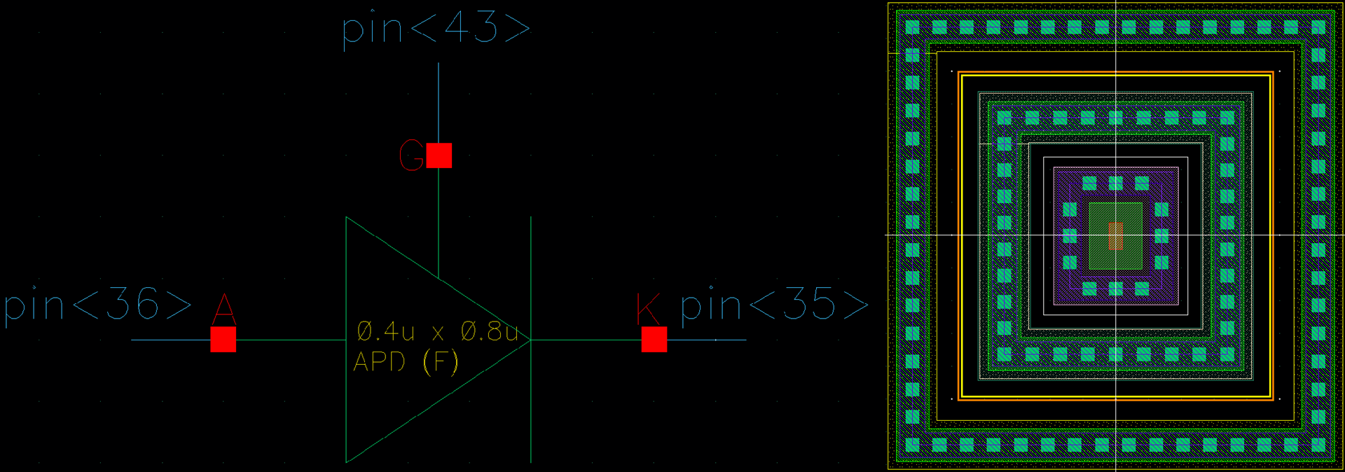
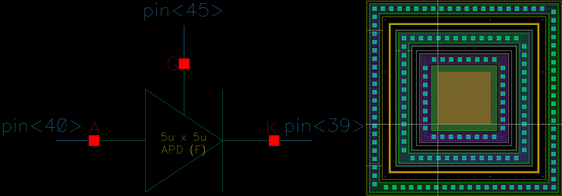
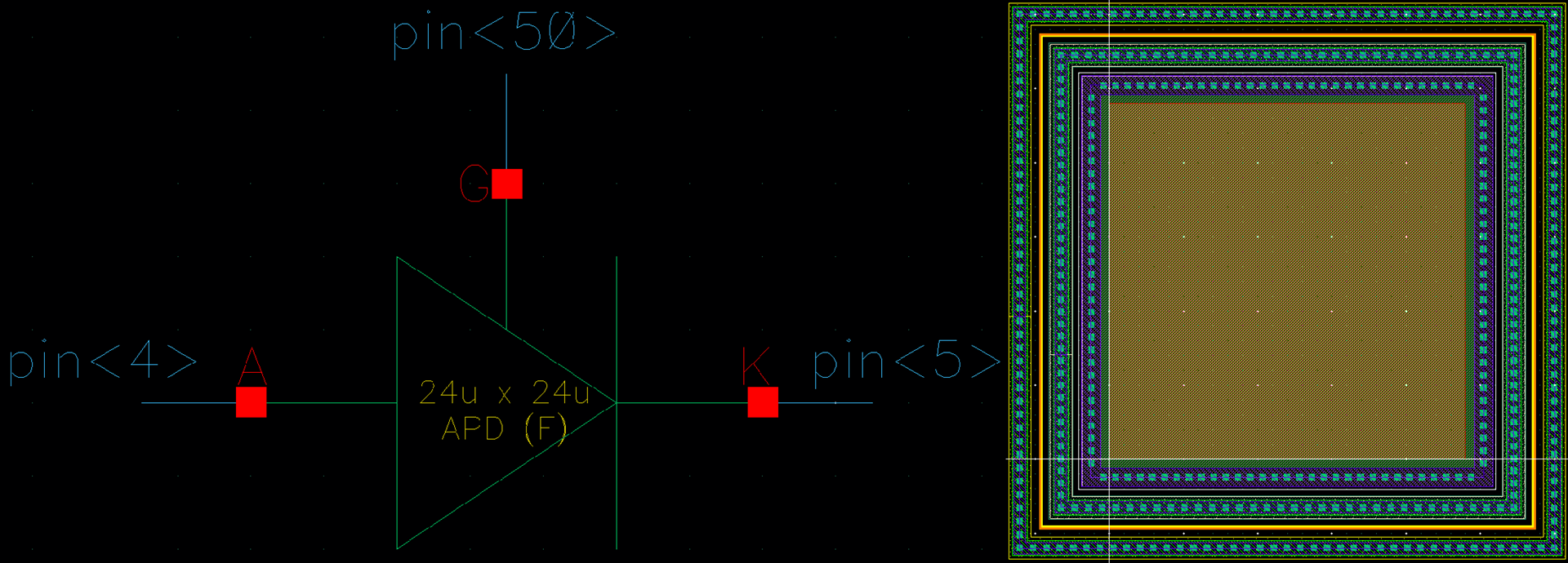
guard rings of the following sizes: 24u x 24u, 5u x 5u, 0.4u x 0.8u
·
Single 24u x 24u APD
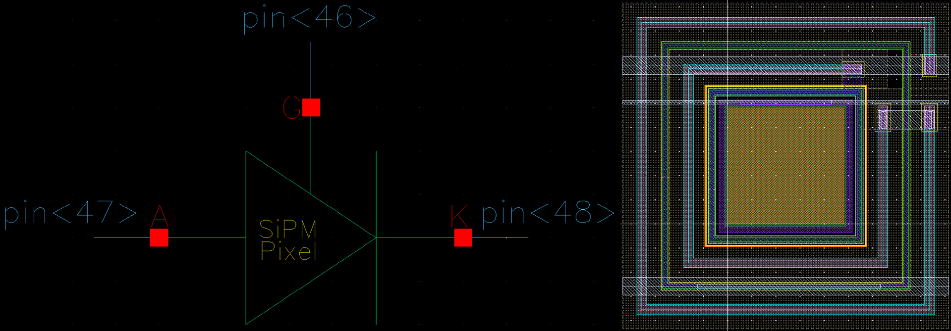
with resistor – SiPM (Silicon Photomultiplier) Pixel
·
16x16
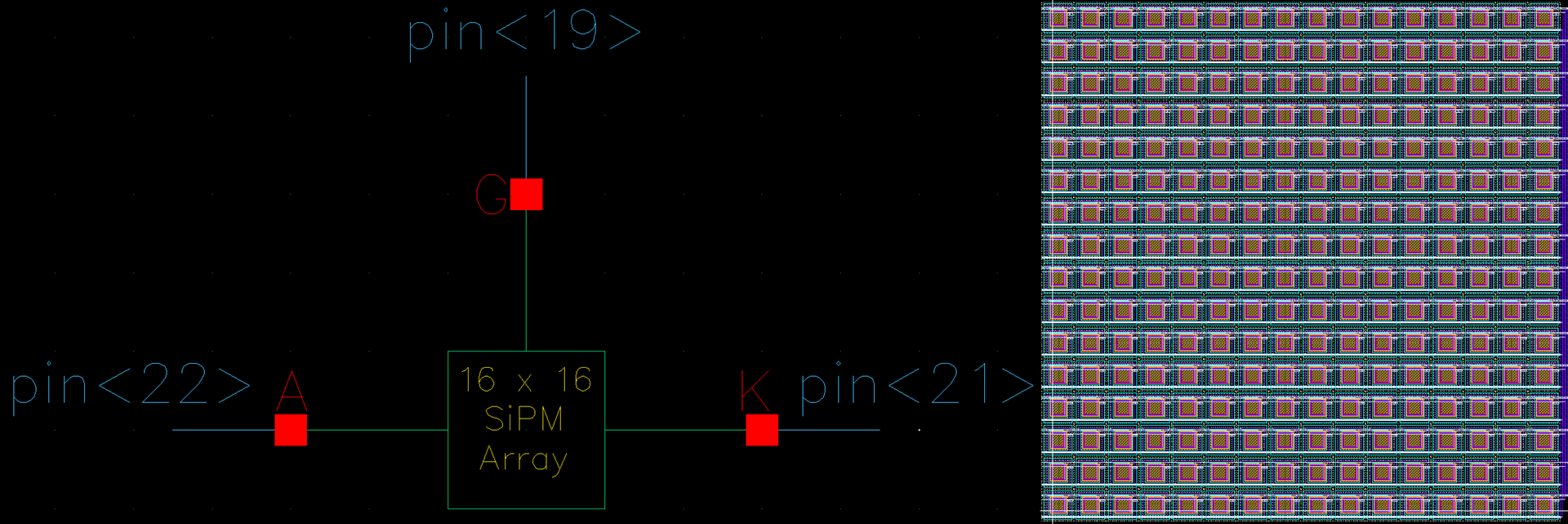
SiPM array of the 24u APD with resistor (SiPM Pixel)
·
Single
output stage of FTD (Fast Transient Digitizer)
·
TIA
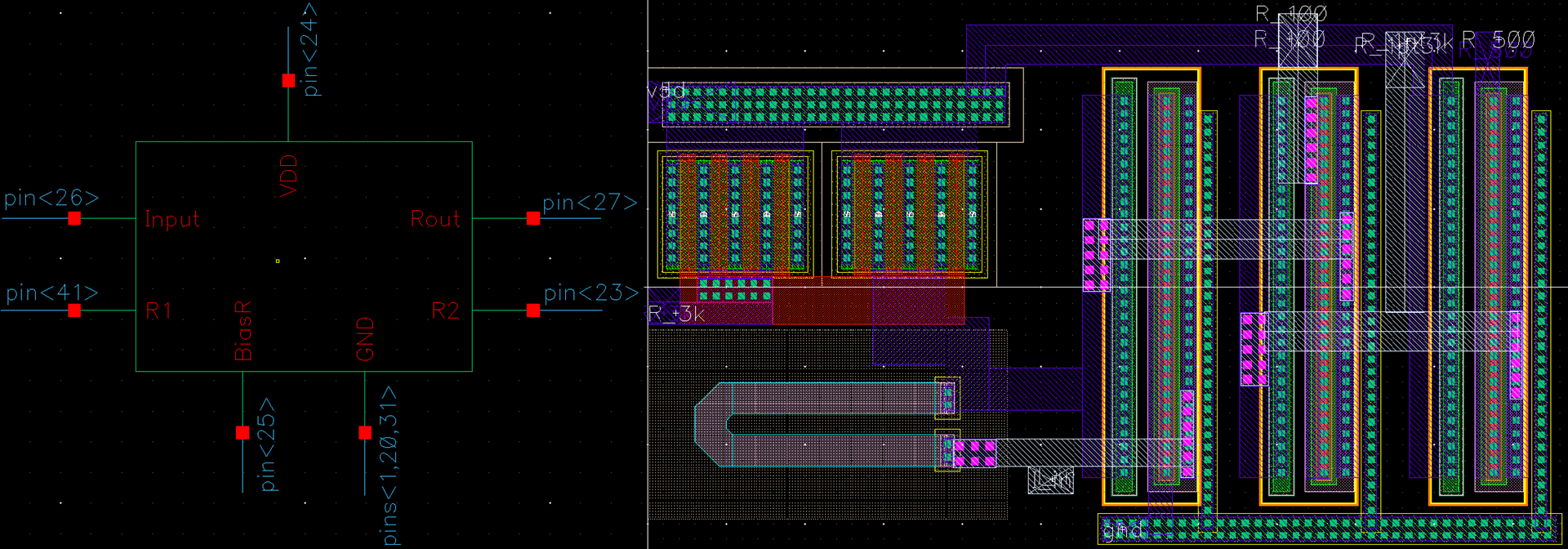
(Transimpedance Amplifier) with source follower
output
·
TIA
with BJT output
·
Low
power DSM (Delta-Sigma Modulator)
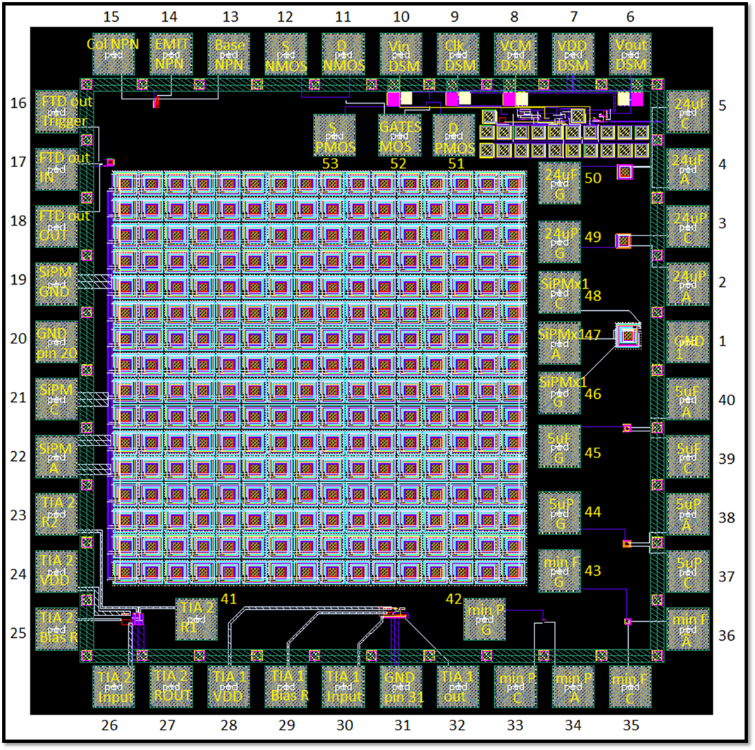
Pad Frame/Key (click for a larger image)
Pin Table
|
Pin # |
Name on Pad Key |
Pin Description |
|
1 |
GND 1 |
Ground |
|
2 |
24uP A |
24u x 24u (Maximum Size)
Partial Guard Ring APD – Anode (A) |
|
3 |
24uP C |
24u x 24u (Maximum Size)
Partial Guard Ring APD – Cathode (K) |
|
4 |
24uF A |
24u x 24u (Maximum Size) Full
Guard Ring APD – Anode (A) |
|
5 |
24uF C |
24u x 24u (Maximum Size) Full
Guard Ring APD – Cathode (K) |
|
6 |
Vout DSM |
DSM - Output
Voltage |
|
7 |
VDD DSM |
DSM - Supply
Voltage |
|
8 |
VCM DSM |
DSM - Common Mode
Voltage |
|
9 |
Clk DSM |
DSM – Clock |
|
10 |
Vin DSM |
DSM - Input Voltage |
|
11 |
D NMOS |
10u/1u NMOS – Drain |
|
12 |
S NMOS |
10u/1u NMOS –
Source |
|
13 |
Base NPN |
NPN BJT – Base |
|
14 |
EMIT NPN |
NPN BJT – Emitter |
|
15 |
Col NPN |
NPN BJT – Collector |
|
16 |
FTD out Trigger |
FTD – Trigger |
|
17 |
FTD out IN |
FTD – Input |
|
18 |
FTD out OUT |
FTD – Output |
|
19 |
SiPM GND |
16x16 SiPM Array -
Guard Ring / Substrate |
|
20 |
GND pin 20 |
Ground |
|
21 |
SiPM C |
16x16 SiPM Array - Cathode
(K) |
|
22 |
SiPM A |
16x16 SiPM Array - Anode
(A) |
|
23 |
TIA 2 R2 |
TIA 2 – Resistor
(R2) |
|
24 |
TIA 2 VDD |
TIA 2 – Supply
Voltage |
|
25 |
TIA 2 Bias R |
TIA 2 – Bias
Resistor |
|
26 |
TIA 2 Input |
TIA 2 – Input |
|
27 |
TIA 2 ROUT |
TIA 2 – Output
Resistor |
|
28 |
TIA 1 VDD |
TIA 1 – Supply
Voltage |
|
29 |
TIA 1 Bias R |
TIA 1 – Bias
Resistor |
|
30 |
TIA 1 Input |
TIA 1 – Input |
|
31 |
GND pin 31 |
Ground |
|
32 |
TIA 1 out |
TIA 1 – Output |
|
33 |
min P C |
0.4u x
0.8u (Minimum Size) Partial Guard Ring APD – Cathode (K) |
|
34 |
min P A |
0.4u x 0.8u (Minimum Size)
Partial Guard Ring APD – Anode (A) |
|
35 |
min F C |
0.4u x 0.8u (Minimum Size) Full
Guard Ring APD – Cathode (K) |
|
36 |
min F A |
0.4u x 0.8u (Minimum Size) Full
Guard Ring APD – Anode (A) |
|
37 |
5uP C |
5u x 5u Partial Guard Ring APD
– Cathode (K) |
|
38 |
5uP A |
5u x 5u Partial Guard Ring APD
– Anode (A) |
|
39 |
5uF C |
5u x 5u Full Guard Ring APD –
Cathode (K) |
|
40 |
5uF A |
5u x 5u Full Guard Ring APD –
Anode (A) |
|
41 |
TIA 2 R1 |
TIA 2 – Resistor
(R1) |
|
42 |
min P G |
0.4u x 0.8u (Minimum Size)
Partial Guard Ring APD - Guard Ring / Substrate |
|
43 |
min F G |
0.4u x 0.8u (Minimum Size) Full
Guard Ring APD - Guard Ring / Substrate |
|
44 |
5uP G |
5u x 5u Partial Guard Ring APD - Guard Ring / Substrate |
|
45 |
5uF G |
5u x 5u Full Guard Ring APD - Guard Ring / Substrate |
|
46 |
SiPMx1 G |
SiPM Pixel - Guard Ring / Substrate |
|
47 |
SiPMx1 A |
SiPM Pixel – Anode (A) |
|
48 |
SiPMx1 C |
SiPM Pixel – Cathode (K) |
|
49 |
24uP G |
24u x 24u (Maximum Size)
Partial Guard Ring APD - Guard Ring / Substrate |
|
50 |
24uF G |
24u x 24u (Maximum Size) Full
Guard Ring APD - Guard Ring / Substrate |
|
51 |
D PMOS |
10u/1u PMOS – Drain |
|
52 |
GATES MOS |
10u/1u NMOS/PMOS –
Gate |
|
53 |
S PMOS |
10u/1u PMOS –
Source |
* NOTE: all gnd! connections for non-APD structures are connected to
pin<1>, pin<20>, and pin<31>.
Pin Tables
NMOS/PMOS
|
Component |
Drain |
Source |
Gate |
Body |
|
10u/1u NMOS |
Pin 11 |
Pin 12 |
Pin 52 |
Ground Pins 1, 20, 31 |
|
10u/1u PMOS |
Pin 51 |
Pin 53 |
Pin 52 |
Source Connected |
NPN BJT
|
Component |
Base |
Emitter |
Collector |
Substrate |
|
24u Area NPN BJT |
Pin 13 |
Pin 14 |
Pin 15 |
Ground Pins 1, 20, 31 |
APD’s
|
Component |
Anode (A) |
Cathode (K) |
Guard Ring /
Substrate (G) |
|
0.4u x 0.8u (Minimum
Size) Partial Guard Ring APD |
Pin 34 |
Pin 33 |
Pin 42 |
|
0.4u x 0.8u (Minimum
Size) Full Guard Ring APD |
Pin 36 |
Pin 35 |
Pin 43 |
|
5u x 5u Partial Guard Ring
APD |
Pin 38 |
Pin 37 |
Pin 44 |
|
5u x 5u Full Guard Ring APD |
Pin 40 |
Pin 39 |
Pin 45 |
|
24u x 24u (Maximum
Size) Partial Guard Ring APD |
Pin 2 |
Pin 3 |
Pin 49 |
|
24u x 24u (Maximum
Size) Full Guard Ring APD |
Pin 4 |
Pin 5 |
Pin 50 |
|
SiPM Pixel |
Pin 47 |
Pin 48 |
Pin 46 |
|
16 x 16 SiPM Array |
Pin 22 |
Pin 21 |
Pin 19 |
* SiPM Pixel comprised of 24u x 24u Full Guard
Ring APD w/ a serpentine poly-resistor
* 16 x 16
SiPM Array comprised of 256 SiPM Pixels
FTD
|
Component |
Trigger |
In |
Out |
Ground |
|
FTD |
Pin 16 |
Pin 17 |
Pin 18 |
Ground Pins 1, 20, 31 |
TIA 1
|
Component |
VDD |
Bias R |
Input |
Out |
Ground |
|
TIA w/ Source
Follower Output |
Pin 28 |
Pin 29 |
Pin 30 |
Pin 32 |
Ground Pins 1, 20, 31 |
TIA 2
|
Component |
R2 |
VDD |
Bias R |
Input |
Rout |
R1 |
Ground |
|
TIA w/ BJT Output |
Pin 23 |
Pin 24 |
Pin 25 |
Pin 26 |
Pin 27 |
Pin 41 |
Ground Pins 1, 20, 31 |
DSM
|
Component |
Vout |
VDD |
VCM |
Clock |
Vin |
Ground |
|
DSM |
Pin 6 |
Pin 7 |
Pin 8 |
Pin 9 |
Pin 10 |
Ground Pins 1, 20, 31 |
NMOS/PMOS
10u/1u NMOS
10u/1u PMOS
NMOS/PMOS
|
Component |
Drain |
Source |
Gate |
Body |
|
10u/1u NMOS |
Pin 11 |
Pin 12 |
Pin 52 |
Ground Pins 1, 20, 31 |
|
10u/1u PMOS |
Pin 51 |
Pin 53 |
Pin 52 |
Source Connected |
NPN BJT
24u Area NPN BJT
NPN BJT
|
Component |
Base |
Emitter |
Collector |
Substrate |
|
24u Area NPN BJT |
Pin 13 |
Pin 14 |
Pin 15 |
Ground Pins 1, 20, 31 |
APD’s
0.4u x 0.8u (Minimum Size) Partial Guard Ring APD
0.4u x 0.8u (Minimum Size) Full Guard Ring APD
5u x 5u
Partial Guard Ring APD
5u x 5u
Full Guard Ring APD
24u x 24u (Maximum Size) Partial Guard Ring APD
24u x 24u (Maximum Size) Full Guard Ring APD
SiPM Pixel
16 x 16 SiPM Array
APD’s
|
Component |
Anode (A) |
Cathode (K) |
Guard Ring / Substrate (G) |
|
0.4u x 0.8u (Minimum Size) Partial Guard Ring APD |
Pin 34 |
Pin 33 |
Pin 42 |
|
0.4u x 0.8u (Minimum Size) Full Guard Ring APD |
Pin 36 |
Pin 35 |
Pin 43 |
|
5u x 5u Partial Guard Ring APD |
Pin 38 |
Pin 37 |
Pin 44 |
|
5u x 5u Full Guard Ring APD |
Pin 40 |
Pin 39 |
Pin 45 |
|
24u x 24u (Maximum Size) Partial Guard Ring APD |
Pin 2 |
Pin 3 |
Pin 49 |
|
24u x 24u (Maximum Size) Full Guard Ring APD |
Pin 4 |
Pin 5 |
Pin 50 |
|
SiPM Pixel |
Pin 47 |
Pin 48 |
Pin 46 |
|
16 x 16 SiPM Array |
Pin 22 |
Pin 21 |
Pin 19 |
* SiPM Pixel comprised of 24u x 24u Full Guard
Ring APD w/ a serpentine poly-resistor
* 16 x 16
SiPM Array comprised of 256 SiPM Pixels
FTD
Fast Transient Digitizer
FTD
|
Component |
Trigger |
In |
Out |
Ground |
|
FTD |
Pin 16 |
Pin 17 |
Pin 18 |
Ground Pins 1, 20, 31 |
TIA 1
TIA w/ Source Follower Output
TIA 1
|
Component |
VDD |
Bias R |
Input |
Out |
Ground |
|
TIA w/ Source
Follower Output |
Pin 28 |
Pin 29 |
Pin 30 |
Pin 32 |
Ground Pins 1, 20, 31 |
TIA 2
TIA w/ BJT Output
TIA 2
|
Component |
R2 |
VDD |
Bias R |
Input |
Rout |
R1 |
Ground |
|
TIA w/ BJT Output |
Pin 23 |
Pin 24 |
Pin 25 |
Pin 26 |
Pin 27 |
Pin 41 |
Ground Pins 1, 20, 31 |
DSM
Delta-Sigma Modulator
DSM
|
Component |
Vout |
VDD |
VCM |
Clock |
Vin |
Ground |
|
DSM |
Pin 6 |
Pin 7 |
Pin 8 |
Pin 9 |
Pin 10 |
Ground Pins 1, 20, 31 |
Last Updated Wednesday, June 15, 2017
