Email and Errata for CMOS Circuit
Design, Layout, and Simulation
Errata
Typos found in the 4th Edition of CMOS Circuit Design, Layout, and Simulation, ISBN–13: 9781119481515, published July, 2019.
page 30 - problem 1.22 "amplitude" is spelled wrong
page 88 - second line from the bottom of the page change "fin's height plus two times the fin's width." to "fin's width plus two times the fin's height."
page 265 - above Eq. (8.80) change "see pages 792-793" to "see pages 821-822"
page 305 - arrow in Fig. 9.32 should be brought to the front
page 308 - middle of the page change "pages 151 and 297" to "pages 154 and 304"
page 349 - change the beginning of the last sentence from "when the input is VIH and" to "when the input is VIL and"
page 470 - end of first paragraph, change "3.125" to "3.25"
page 499 - change, just above Example 17.1, "function" to "functions"
page 509 - second line from the bottom of the page change "37 mV" to "39.6 mV"
page 510 - 9th line down M should be 50, not 36, as seen in the following equation
page 515 - third line in third paragraph, last word, change "successful" to "successive"
page 525 - in the caption for Fig. 17.37a change "M = 98" to "M = 97"
page 535 - 7th line from the bottom change "0.25 V" to "0.28 V"
page 541 - Figure 18.13 the "out2" arrow is pointing to the wrong trace
page 554 - change MN to MN+1 in Fig. 18.38
page 959 - change "wth" to "with" in the caption for Fig. 28.6
page 1126 - the label for Eq. (31.22) should be shifted to the right a little
page 1177 - second line from the bottom change "capacitor" to "capacitors"
page 1178 - change, in the line above Eq. (32.8) "know" to "knowing"
page 1187 - 7th line from the bottom, the sentence starting "The current flowing in the inductor....returned to the power supply." is misleading. While the current flowing in the inductor, due to the energy stored in the inductor, is returned through the diode to the power supply node, this current does not charge (return energy to) the power supply.
page 1189 - 12th line from the bottom change "form" to "from"
A
few of the email questions, and responses, received for the third edition are
listed below.
1. How do you calculate the
channel-length modulation parameter, λ,
for a 180 nm process?
2. Is gm (and thus device fT) independent of overdrive voltage in
nanometer CMOS?
3. In Ch. 20, on page 629 in Fig
20.22, I am unclear of the reason Vreg…
4. Why do you call the reference
in Fig. 20.14 a Beta-Multiplier Reference (BMR)
5. Reading about "hot
carriers" I found your explanation that this had to do…
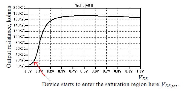
6. On pages 144 and 145 you
discuss how VDS,sat is not
exactly VGS - VTHN.
8. How do we define VDS,sat for short-channel MOSFETs?
9. SF gain calculations on page
670 and 691
10. In Fig. 26.41 it says this is
NOT the way to implement GE in ...
11. In Fig. 26.16 can’t we remove
the φ2 switches on the
bottom of C2 for better operation?
12. I tried to hand calculate the
values in Table 9.2 using the short channel equations...
13. I had a quick question on
deriving voltage gain on common-source amp with source degeneration.
14. Are the PMOS loads in Fig.
24.21 called "composite cascodes?"
15. What does "feature size"
mean?
16. Would you provide a reference
for the Miller Effect?
17. Why does the spectrum
analyzer block diagram...?
18. In the square-law equation
you use (VDS - VDS,sat)
while others...
19. On page 1146 in the third paragraph
you indicate you can't use the
...
20. What is the layer "elec" in the NCSU setups for the C5 process?
21. I have several questions
about the voltage regulator presented in Sec. 24.5.
22. Please comment on the
definition of VOH and VOL for the inverter, Ch. 11?
23. The value of e (=2.718) is used to size up the widths
in the cascade of inverters for...
24. When I simulate an analog
circuit using LTspice I get jagged sinewaves. What’s going on?
25. I have one question...you
designed all of your circuits for nominal process variations.
26. Is there a way to speed up LTspice
simulations?
27. What is the best thing for me
to focus on to improve the matching of two components?
28. I copied the op-amp in Fig.
24.44 but using a 130 nm process...
30. On page 525, Eq. (18.3), you
assume M1 is in saturation when the Schmitt trigger switches...
31. How would
one implement a current mirror with a non-integer ratio and good matching?
32. I have a
question about the MOS switching resistance in Sec. 10.1.
34. In the
indirect compensation scheme used in the book you use 1 capacitor...
35. Would you show how to take the
derivative of Q'b0 to get Q'b0/2T as seen in Sec. 9.1.3?
37. The
equation for the bandgap energy of Si given by Eq. (23.21) is a little...
38. You mention that to improve the CMRR of a diff-amp the capacitance...
39. Would you show the detailed algebra resulting in Eqs. (30.31) and (30.32)?
41. If I use LTspice do I have to
modify the SPICE models that I download from MOSIS?
43. Would you please show how to derive the lock time, pull-in time, etc. for the charge pump PLLs in Ch. 19?
Typos found in the
third edition of CMOS Circuit Design, Layout, and Simulation, ISBN–13: 978-0-470-88132-3, published August, 2010.
How to tell the
printing number is found here.
Typos found in the
4th, and later, printings of the 3rd Edition
pages 18-19 – the netlists in Figs. 1.21
and 1.22 changed from .tran 10u 30m to .tran 10u 16m
page 25 – the netlist describes a circuit where the position of the switch and resistor, in Fig. 1.31, are swapped (same results since they are in series)
page 187 – third line from the
bottom change Sec. 2.5 to Sec. 2.6
page 256 – the last term in Eq.
(8.69) should be multiplied by Rs
page 282 – 15th line
from the bottom change mag(vd34) to
mag(vd24)
page 298 – in Fig. 9.32 move the arrow head a little to the right (to VDS = 50 mV)
page 299 – in Fig. 9.34 the later versions of the BSIM4 model simulations result in an fT of 3.7 GHz rather than 6 GHz
page 447 – change 8,192 to 4,096
page 531 – in Fig. 18.11 modify the waveform sketch to have cleaner exponential shapes between the switching times
page 543 – fourth line from the top change Fig. 18.13 to Fig. 18.33
page 545 – in Fig. 18.38 change CN-1 to CN and CN to Cload then the top of (new) CN swings between (N + 1) ·VDD – N·VTHN and N ·(VDD – VTHN). The final output voltage across Cload is then (N + 1)· (VDD -VTHN )
page 579 – Eq. (19.59) isn't correct. See the correct equation from the derivation found here. Also see email question 43 seen above.
page 649 – change, in Fig.
20.45’s caption, “the current sourced by the
NMOS.” to “the current sunk by the NMOS.”
page 775 – Fig. 24.3
change caption from "(b) its gain (the derivation
of (a))" to "(b) its gain (the derivative
of (a))".
page 780 – second line from the bottom change 1/gmn to 1/gm2
page 782 – fourth line down change (Rz = 1/gm1) to (Rz = 1/gm2 = 1/gmp in Fig. 24.8), and for rest of the page change gm1 to gm2
page 803 – last line of the
second paragraph change M11 to M12
page 851 – fourth line from the top change "(as discussed in Ch. 6)." to "(as discussed in Ch. 5)."
page 1044 – in Fig. 30.19 change 2-4, 2-8, and 2-16 to 2-3, 2-4, and 2-5
page 1096 – top of the page, change Problems to PROBLEMS
page 1172 – change the entry "Twin tub, 31" to "Twin well, 31, 52-55"
Typos
fixed in the 4th printing of the 3rd Edition
front inside cover – in
the Multipliers table add “exa” (= 1015)
and “peta” (= 1018), remove the comment that “atto”
or “a” isn’t used in SPICE (it is used in modern simulators), change the
spelling of “terra” to “tera”, change the
relative dielectric constant of Si02 from 3.97 to 3.9, and change the listing of SiN3 to Si3N4
(silicon nitride) with a relative dielectric constant of 7.5.
page xxx – move
the “……” between Sec. 31.9.2’s title and page number to between Sec. 31.9’s
title and page number
page 26 – change
the sign of the phase shift in Eq. (1.16) as seen fixed here
page 107 – in Fig. 5.2 swap
values for L and W (two places) and then remove the “10k” in the SPICE
statement for r1 as seen fixed here
page 114 – tenth line
down change 3.97 to 3.9
page 132 – the line below Eq.
(6.2) change 3.97 to 3.9
page 215 – fourth line in the
second paragraph from the bottom of the page change “…DC source, VDC , is VDC ” to “…DC
source, VDC , is V 2DC
”
page 221 – second line from the
bottom change “tan-12ðf/f3dB”
to “tan-1f/f3dB”
page 250 – near the middle of
the page change “1018” to “10–18”
page 287 – change “constan” to “constant” at
the end of Eq. (9.26)
page 346 – in the first
sentence, last word, change “seven” to “nine”
page 835 – the + and –
terminals of A1 in both Figs. 25.9 and 25.10 should be swapped
page 952 – Figure 28.23b the
decimal in .5 is spaced too far away from the “5”, it’s under the “s” in LSBs
(yes, very minor ;-)
page 1076 – in Fig. 30.54 change, above
caption, Vout to vout
page 1077 – in Fig. 30.55 change Vin+,
Vin–, Vout+,
Vout–, Vouta, Vouth,
and Vavg to vin+,
vin–, vout+,
vout–, vouta, vouth,
and vavg respectively
page 1101 – fifth line down
change “…will be used later sections…” to “…will be used in later sections…” and tenth line down remove “reducing the effects of noise, ”.
While it is true that feedback reduces an amplifier’s output noise it also
reduces the desired output signal by the same amount, as discussed in Sec.
8.3.2, so no improvement in SNR is realized using feedback.
page 1119 – below the middle of
the page change 1.002 ohm to 1.002 kohm,
second line from the bottom Rbo should be infinite,
not zero (Rbi
and Rbo
are both ideally infinite)
page 1149 – Figure
31.55c and (d) should have the gate of the second transistor moved down to the
drain of the first PMOS as seen fixed here
Typos
fixed in the 3rd printing of the 3rd Edition
page 5
– move the bold line in Fig. 1.5 to the
front to show the location of the cross-sectional view
page 38 – 9th
line from the bottom change "n+ and p+ implants" to "n+ and p+ field implants"
page 65 – first
equation change (2,000·4) to (2,000 + 0.4)
page 144 – third line below Eq.
(6.41) add to the end of the sentence “…over smaller distances, see LDD discussion on the bottom of page 151.”
pages 154-157 – minor modifications to the
BSIM4 models for better modeling of the S/D parasitics, see fix here
page 236 – fix "0" at the
end of Eq. (8.43). The “0” is partially cut-off (yes, very minor ;-).
page 251 –
some changes to make the example clearer are seen here
page 302 – fifth line from the
bottom change RCH to Rch
and then adjust position of Eq. (9.63) label
page 578 – change the (1 + sRC1)
in the numerator of Eq. (19.56) to (1 + sRC1)/C1
page 621 – seventh line down
change “900 mV to 1 V.” to “900 mV to 1.1 V.”
page 625 – last paragraph
change, in two places, “closed loop gain”
to “loop gain”
page 704 – on the right side of
Eq. (21.123) the “1” should also, in addition to the gmnRncas,
be multiplied by ron||rop
page 759 – 7th line
from the bottom change “and that is why the…” to
“and this, combined with the more dominant increase in
the scale current, Is, with temperature, is why the…”
page 767 – add note to Fig.
23.29 reminding that circuits that use feedback can become unstable, see
addition here
page 871 – 8th line
from the bottom change Ac to Acm
page 882 – second line in the
second paragraph change vop,n
to vop,m
page 913 – change, in Fig.
27.6a, “2.4 to 2.6” to “2.48 to 2.52” and in Fig. 27.6b change “2.4” to “2.48”.
page 1013 – shift
(29.104) to the right so it’s aligned with the other equation numbers
page 1065 – fifth and sixth lines in first
paragraph change 30.30 and 30.37 to 30.34 and
30.35 respectively
page 1069 – line below Eq. (30.60) change (VCM
< vin < 3VCM /2) to (VCM /2 < vin < 3VCM /2)
page 1071 – 9th line down change
“weighting, Eq. (30.27),” to simply
“weighting”
page 1113 –
four lines above Eq. (31.28) change “…amplifier, AOL, and the…” to “…amplifier
and the…”
pages 1115, 1116, 1118, 1122, 1123, 1130,
1131, and 1132 – change the figures and equations to use vsg
for the PMOS instead of vgs (flip current sources and the +
and – around). It’s correct the way it is but it’s inconsistent with the rest
of the book, see changes here.
page 1134 – M1 in Fig. 31.37a should be a
PMOS device, remove ro3/ro4
in two places in the first equation
page 1140 – first
and second equations on the page change RI to Ri
page 1141 – 9th line
from the bottom change "closed gain, ACL" to
"closed-loop gain, ACL
"
page 1143 – line below heading Amplifiers
with Gain change “Figs. 31.46 or 31.47” to “Figs. 31.45b or 31.47”
page 1144 – in
Fig. 31.48 change Vbias2 to Vbias4 in two places
page 1147 – 5th
line down the reduction in W doesn’t affect (ideally) AOL
(see Eq. [9.61]) but reducing W does reduce the noise in the drain
current (as indicated).
page 1163 – add
“Feature size, F, 444” to the index
Typos
fixed in the Revised 2nd Edition, ISBN–13:
978–0–470–22941–5, published November, 2007.
Typos
fixed in the 4th printing of the Revised 2nd Edition
page 3 –
the words “die” and “dice” should be swapped in
the sentence at the top of Fig. 1.2
page 26 – Vin
and Vout are transposed in Eqs. (1.14) and (1.15)
pages 154, 156 – for the
BSIM4 models change level=14 to level=54. Not an error but rather an update.
Note that older SPICE simulators still require Level=14 when using the BSIM4
model
page 244 – 2nd
line from the bottom. Change "pronouced" to
"pronounced"
page 251 –
bandwidth for the op-amp’s contribution to noise should be 2 MHz not 1.59 kHz,
see fix here
page 261 – third
line down change 8.5 pA/root(Hz) to 0.85 pA/root(Hz)
page 348 – the term
in Eq. (11.28), (r*l)(Cload) should be 2*(r*l)(Cload)
page 362 – 12th
line down change “then” to “than”
page 500 – Eqs.
(17.17) and (17.18) were derived where M represents the number of times the
feedback path is enabled (as stated). There is an inconsistency, an inversion,
between the two sentences following Eq. (17.18) and the schematic seen Fig.
17.18. Since the feedback path controls a PMOS device this path is enabled when
the DSM output, Q, goes low (so M would represent the number of times Q goes
low). To eliminate the inconsistency we could add an inverter to the output of
the DSM in Fig. 17.18 so that M represents the number of times the DSM output
goes high and thus the number of times M3 is enabled. the right side of Eq.
(17.21) should not have the Ccup in it since M4 is a
source follower and isolates the two capacitors. Eq. (17.22) should be modified
accordingly.
page 600 – 3rd
line from the bottom change the sentence “Notice that the static phase error.”
to “Notice the static phase error.” (Remove “that”).
page 703 – remove
the extra period at the end of Figure 21.54’s caption.
page 840 – in Fig.
25.16 swap the op-amps’ + and – inputs so there is negative feedback.
page 866 – 5th
and 6th lines down change “current variations vary” to “how the
current varies”
page 870 – 9th
line down change “M1” to “the 200/1 PMOS”
pages 879, 881, 883, and
885 – Figures 26.22, 26.26, 26.29, and 26.33 remove the wire shorting the op-amp’s
+ and – inputs
index
– the index entry Decoder, 329,
43-34, 447, … should be changed to Decoder, 329, 430, 433, 447, …,
Typos
fixed in the 3rd printing of the Revised 2nd Edition
page 411 –
second paragraph, second sentence change “The dark dots indicate and, thus, a
failing chip.” to “The dark dots indicate defects and thus bad chips.”
page 486 – Figure
17.3 the word “add” should be “remove”
page 917 – eighth
line down change 2.49–2.51 V to 2.45–2.55 V
page 928 – fifth
line, second paragraph, the x–input is 0.25 not 0.5 as indicated (the
calculation for the location of point A is correct). In the same paragraph,
seventh line, point B is at -1.8V not 1.8 V
page 950 – Fig.
28.21b the decimal point is missing in front of the ½ LSB DNL, that is, 5
should be .5
index
– the index entry for
Saturation region is listed twice, separated by Salicide
Typos
fixed in the 2nd printing of the Revised 2nd Edition
page 18 –
bottom of the page replace: - 0.294
with - 0.119, - 16.85 with - 6.82, and the time delay in Eq. (1.9), - 234 us
with - 95 us
page 42 –
second paragraph, second line “determining” is misspelled
page 53 –
the triple–well figure should be 2.24d (not 2.24c), change
in first paragraph “can be used, Fig. 2.24c.” to “can be used, Fig. 2.24d.”
page 54 –
replace “Being able use the” with “Being able to use the”
page 61 –
second line change “capacitance for metal1” to “capacitance
for metal2”
page 77 –
Fig. 3.23 should only have 6 pads on a side not 7 (so the
total number of pads is 24 not 28)
page 686 – 14th
line down change “and to eliminate the” to “and to eliminate, or more correctly
to reduce, the”
page 687 – in Eq.
(21.78) Av1 should be - gm1*ro/2. This means, in Ex. 21.12, that Av1 = - 3.75, tau_in = 1.16 ns, and thus fin = 137 MHz.
Typos fixed during the 2nd, 3rd,
and 4th printings of the 2nd Edition, ISBN–13: 978–0–471–70055–5,
published November, 2004.
page 25 –
swap vin and vout in Fig. 1.25 (vout < vin)
page 66 –
the pulse delay in the SPICE netlist should be 50p not 5n
page 85 –
Figure 4.2(f) subtitle should indicate (e) not (g)
page 86 –
last line in second paragraph change "select" to
"active"
page 88 –
figure 4.4, there shouldn't be an oxide above the silicided
MOSFET S/D
page 91 –
there shouldn't be an oxide above the silicided MOSFET S/D
in (h)
page 97 –
in the ninth line from the bottom change "are" to
"area"
page 99 –
the rules show the minimum poly gate extension is 1 where it
should be 1.25.
page 108 – Ex. 5.2
should be a 10k resistor not 50k
page 136 – two
lines above Eq. (6.8) should be changed from "inversion and depletion
cases." to "inversion and accumulation cases."
page 139 – Equation
(6.17) the term Vfb should be Vfp
page 150 – a
parentheses around nkT in Eq. 6.48
page 153 –
indicate, in the last paragraph, that hot indicates carriers with higher than
thermal equilibrium energy
page 174 – change
the spinning direction of the wafer (not wrong just more common)
page 214 –
capitalize Joules in four line
page 216 – modify
figure 8.4 to show the power meter measures V^2,RMS
and that the PSD is this power divided by the resolution of the spectrum analyzer
page 228 – second
line, the word SPICE should be moved to above the figure
page 246 – ninth
line down change 8.50 to 8.51
page 272 – third
line down change series to parallel
page 273 – swap the
+ and – in Fig. 9.6b
page 275 – add 1 uA next to the current source in Fig. 9.9
page 284 – add t
(time) to the bottom two equations (the sinusoids) on the page
page 285 – add a –
in front of 0.5 mV third line down
page 289 – fix
partially hidden VDS on the x–axis in Fig. 9.24
page 295 – indicate
that the temperatures are in Kelvin for Eq. (9.52)
page 297 – indicate
velocity overshoot and other effects cause the gm to increase with vgs
page 309 – problem
9.26 change the 9.1 to 9.2
page 311 –
sixth line from the bottom change "is a 0 V" to "is at 0 V"
page 312 – change
the direction of the pulse in Fig. 10.3b
page 327 – last
line change "fetoprobes" to "femtoprobes"
page 341 – eighth
line down change 11.13 to 11.15, above this change "Latch–Ip" to
"Latch–Up"
page 348 – remove
the 2 at the beginning of Eq. 11.28, and change comments describing RC line
delay and the delay associated with the resistance driving the load C
page 376 – first
line change Evaluating to Increasing
page 380 – Figure
is spelled wrong in Figure 13.9
page 395 – first
line change 13.5ps to 15.75 ps
page 446 – remove
the word trench from the third line
page 447 – 9th line
down change 8–Mbit to 16–Mbit
page 450 – 16th
line down change "VDD is large" to "VDD is small", change
the figure caption to 16.26 instead of 16.27
page 451 – 11th
line from the bottom of the page change "power" to
"current"
page 460 – last
line change "(ideally) ,to" to
"(ideally), to"
page 466 – fix the space
after the word higher in Fig. 16.53
page 468 – change
the direction of electron flow in Fig. 16.56
page 471 –
capitalize NAND in the figure caption of Fig. 16.61
page 488 – fourth
line from the bottom change "constant ,we"
to "constant, we"
page 495 – fourth
line from the bottom should be 17.11b not 17.11a
page 500 – first
line change 17.15 to 17.16
page 513 – Eq.
17.42 the (N – M)/M should be M/(N – M) also change
N/2<=M<=N to 0<=M<=N/2
page 517 – second
paragraph from bottom change “The thermal noise from the capacitors is” to “The
input–referred thermal noise is set by the sampling capacitors and is…”
page 518 – Fig.
17.38 flip the polarity of the offset and first line of second paragraph change
17.33 to 17.36
page 545 – second
to the last line should be (N+1)*VDD – N*VTHN and
N*VDD – N*VTHN
page 546 – fourth
line from the bottom in first paragraph change "A larger capacitor is used
on node A" to "A larger capacitor is used on node B"
page 553 – fourth
line down capabilities is spelled wrong
page 554 – seventh
line down add an s to continue
page 564 – fifth
line from the bottom of the page change 1 mV to 10 mV
page 604 – first
line change 10k to 5k
page 608 – problem
19.04 change "that it" to "that it is"
page 615 – fig.
20.4 change the 210k resistor to 200k
page 620 – tenth
line down change 0.2 to 0.1
page 625 – write
Eq. (20.23) in terms of the overdrive voltage as well (IREF=
and Vov=)
page 637 – second
line from the bottom change "drain" to "drain voltage" also
change the MOSFET references to they refer to the correct MOSFETs
page 639 – Fig.
20.31b change the VGS on the gate of M4 to simply VG
page 649 – Fig.
20.45b fix typo of MB7 to MB6 (second row of PMOS)
page 651 – fourth
line down change Vbias2 to Vbias4
page 657 – eighth
line from bottom fix space in "common– source". In the last line
change from 21.1 to 21.1a
page 667 – remove
square–root brackets in Eq. (21.21)
page 674 – first
line of second paragraph add extra parentheses so they are balanced
page 686 – Eq.
(21.75) should be “V^2inoise =…” instead of “V^2onoise =…”
page 687 – take the
magnitude of the second to the bottom equation
pages 688-690 – equations (21.84)
and (21.85) are only valid when the drain of M2 is connected to a low
impedance. Also, remove noise from M2/M3 in Eqs. (21.79) and (21.80) See here for updated
pages.
page 692 – second
line from the bottom change 600 mV to 500 mV, last paragraph change
all 250 mV to 280 mV
page 694 – remove
M2’s noise contributions in Eq. (21.99), show why in Fig. 21.44
page 697 – replace
the W in Eq. (21.108) with K and indicate K=12.5 (the gm scales linearly with
the MOSFET’s width) and change 530 uA/V to 1.875
mA/v. Change, in the next equation, 1.88k to 533 and 0.84 to 0.95, two lines
below that change 500*0.84 = 420 ==> 52.5 dB to 500*0.95 = 425 ==> 53 dB
pages 697-703 – the
symbols RL and Rload are used interchangeably.
Should, to be consistent, just use Rload.
page 702 – first
equation, move the 1k out of the brackets for a Pload
of 125uW, the Psupply becomes 325uW, the PCE becomes
38%, without bias circuit current PCE is 68%
page 715 – 11th line from
the bottom change “folded– cascode” to “folded–cascode”
page 717 – fix the
formatting of the Iss in Eq. 22.15
page 718 – Ex. 22.4
add an s to components, remove the s on drains, add the word current after
drain, and change 150 uA/V^2 to simply 150 uA/V
page 719 – change,
in Fig. 22.10's caption, 22.10 to 22.4, two lines above Eq. (22.20) change “the
AC current flowing in ro4 is id1.” to “the AC current flowing in M4 is id1.”
(change ro4 to M4)
page 726 – eq.
(22.32) the output noise is divided by A^2d (not the input noise), change the
label on the noise source for M3 in Fig. 22.20 from 6 to 3
page 735 – should
be 3.6 V not 3.65 V and 4.4 V not 4.45 V in Ex. 22.9
page 746 – fourth
line down should indicate Ch. 5 not Ch. 7
page 749 – remove
VSS from Eq. (23.8)
page 762 – Ex. 23.4
should say using Eq. (23.23) not (23.22)
page 765 – add a
start–up circuit to Fig. 23.27
page 766 – change
the simulation and discussion to include the start–up circuit added on the
previous page
page 769 – change
figs. 23.31 and 32 as seen at: http://cmosedu.com/cmos1/book.htm
page 774 – fifth
and seventh lines from the bottom change 900 mV to 930 mV
page 785 – indicate
equation (24.19) is an approximation for |K*Cc/gm1| >> Cc/gmcg
page 790 – Eq.
24.27 should have Acm not Ac
page 791 – fourth
and first lines from the bottom change 20.21, 21.21 to 23.21
page 792 – Eq.
(24.31) should indicate open loop gain AOL not just A
page 793 – last
line remove the square–root bracket can change the gain
to –31.6
page 794 – first
line change gain from 5,000 to 15,600 and gain from 74 dB to 84 dB, also remove
square–root in fourth line down
page 795 – first
line remove the word "and"
page 800 – last
line in second paragraph change fig. 24.38 to fig. 24.39
page 802 – fig.
24.40 shift vm down a little
page 817 – after
equation (24.76) should say CLmin not CLmax
page 820 – fourth
line in second paragraph fix space in "common– source"
page 822 – fourth
line from the bottom should be 2400 fF not 2400 pF
page 851 – fix
caption for Fig. 25.29a
page 873 – change
caption for Fig. 26.14
page 880 – second
line from the bottom fix space in "common– mode"
pages 897-898 – change 10f
to 50f and the 25f to 10f in Fig. 26.50 (not wrong just a little more robust)
page 908 – change
the word edition to volume in problem 26.19
page 919 – fix
space in "cross– coupled" sixth line from top, fix fig. 27.16 caption
page 950 – third
line from the bottom change 011 to 100
page 1018 – problem 29.6
change "Fig. P29.6" to "Fig. 29.52"
page 1019 – problem 29.7
change "5 mA" to "5 uA"
augmented index in second
and later printings
Sorry,
no typo list for the 1st Edition, ISBN–13: 978-0-780-33416-8,
published August, 1997.
However,
the 1st Edition’s supporting material is available in CMOS_1e.zip or CMOS_1e.rar