The
value of e (=2.718) is used to size
up the widths in the cascade of
inverters for driving large load capacitance with minimum delay
in
Ch. 11. However, I have seen others
use 3.59 as the ideal multiplication factor. Would you please comment?
Yes,
let’s look at the SPICE simulated
delays of the buffers seen in Fig. 11.20 (A
= e) from Ex. 11.8 and Fig. 11.21 (A = 8) from Ex. 11.9.
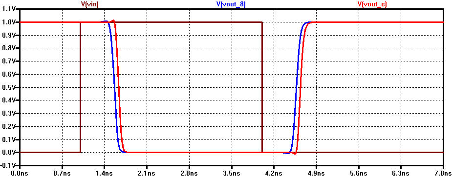
The
hand calculations in these examples
indicated that using an area value, A,
of e should result in less delay
than
using a value of 8.
However,
as seen above this isn’t the
case. We have the constraint that the number of inverters used is an
integer
which affects the
selection
of A. Again, simulations are
invaluable for estimating delay. Hand
calculations only get the designer near a good design.
Okay,
let’s compare the above results
to a buffer design using an area factor of 3.59 with N
= 7. The value of 3.59 results from not
assuming
that the first term in Eq.
(11.25) is small, and thus negligible, when solving for N
(more exact but more useful??? See
comments
below.).
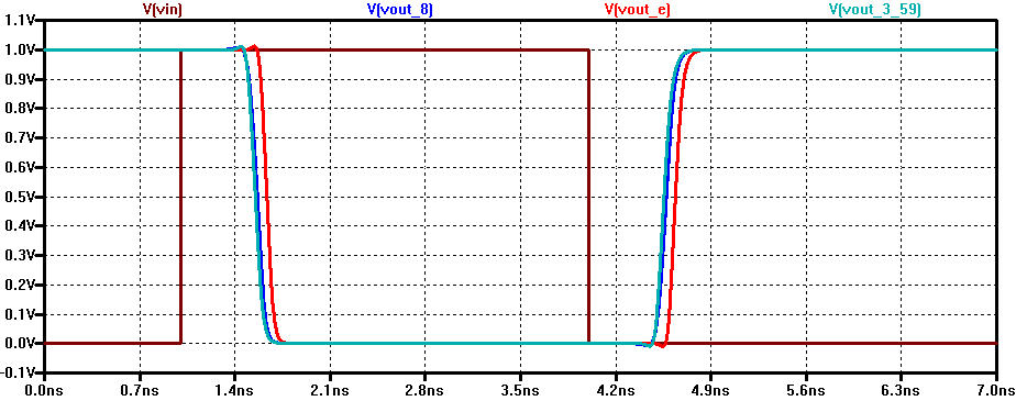
As
can be seen we get a small reduction
in delay using 3.59. However, let’s see what happens if we reduce the
last
inverter’s widths in
Fig.
11.21 by 4, that is, from
81,920/40,960 to 20,480/10240.
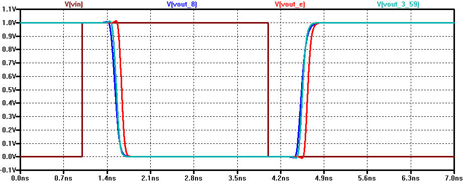
We
get a much smaller buffer and even
slightly less delay than when A =
3.59!
Why?
As mentioned above we have a
constraint to use an integer number of inverters. This affects the
ideal
selection of A. We can,
however,
simply reduce the widths of
the last inverter to compensate for this constraint (reducing the
layout size
without much change
in
delay). In any case it’s academic to focus on
a specific optimum area
factor for a buffer design since a wide range will give very
similar
performances. Again, layout
size is often an important factor.
So,
why was e derived as the optimum A
in Ch. 11? Why not derive 3.59? The derivation using e
is clean and we arrive at equations,
e.g.,
Eq. (11.25), that can be directly
applied to buffer design. Again, as mentioned in Ch. 11, small A values (say < 4) are rarely used
in
buffer designs.
Additional
Reading
Hedenstierna,
N. and Jeppson, K. O.,
“CMOS Circuit Speed and Buffer
Optimization,” IEEE Trans. on CAD,
Vol. CAD-6, No. 2, pp. 270-281, March 1987.