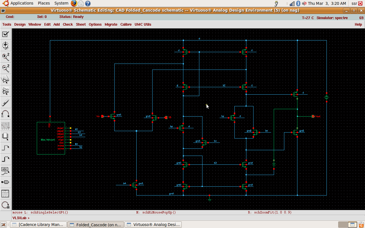
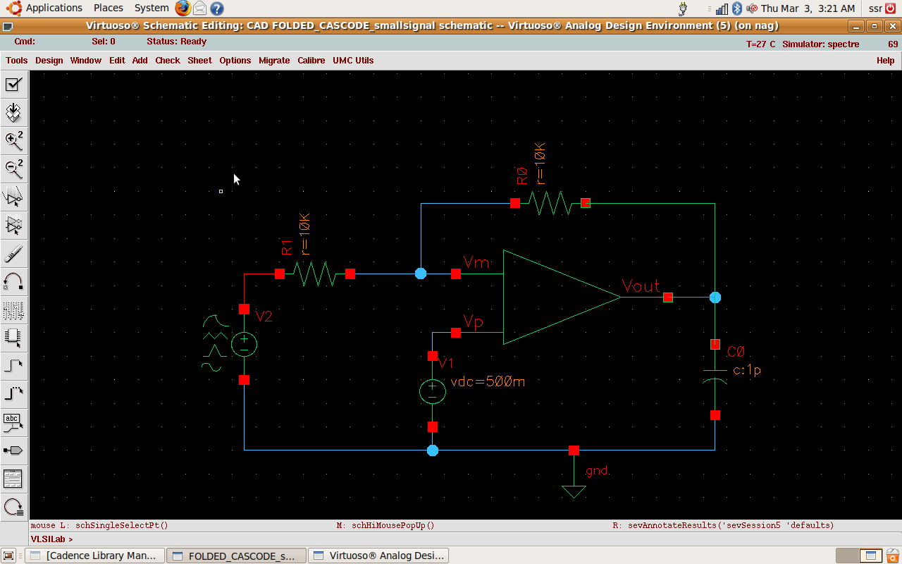
I
copied the op-amp in Fig. 24.44 but
using a 130 nm process. I get a gain margin of 7 dB and a phase margin
of 54
degrees using Cc
= 250 fF
and Cload
= 1 pF. My problem is I
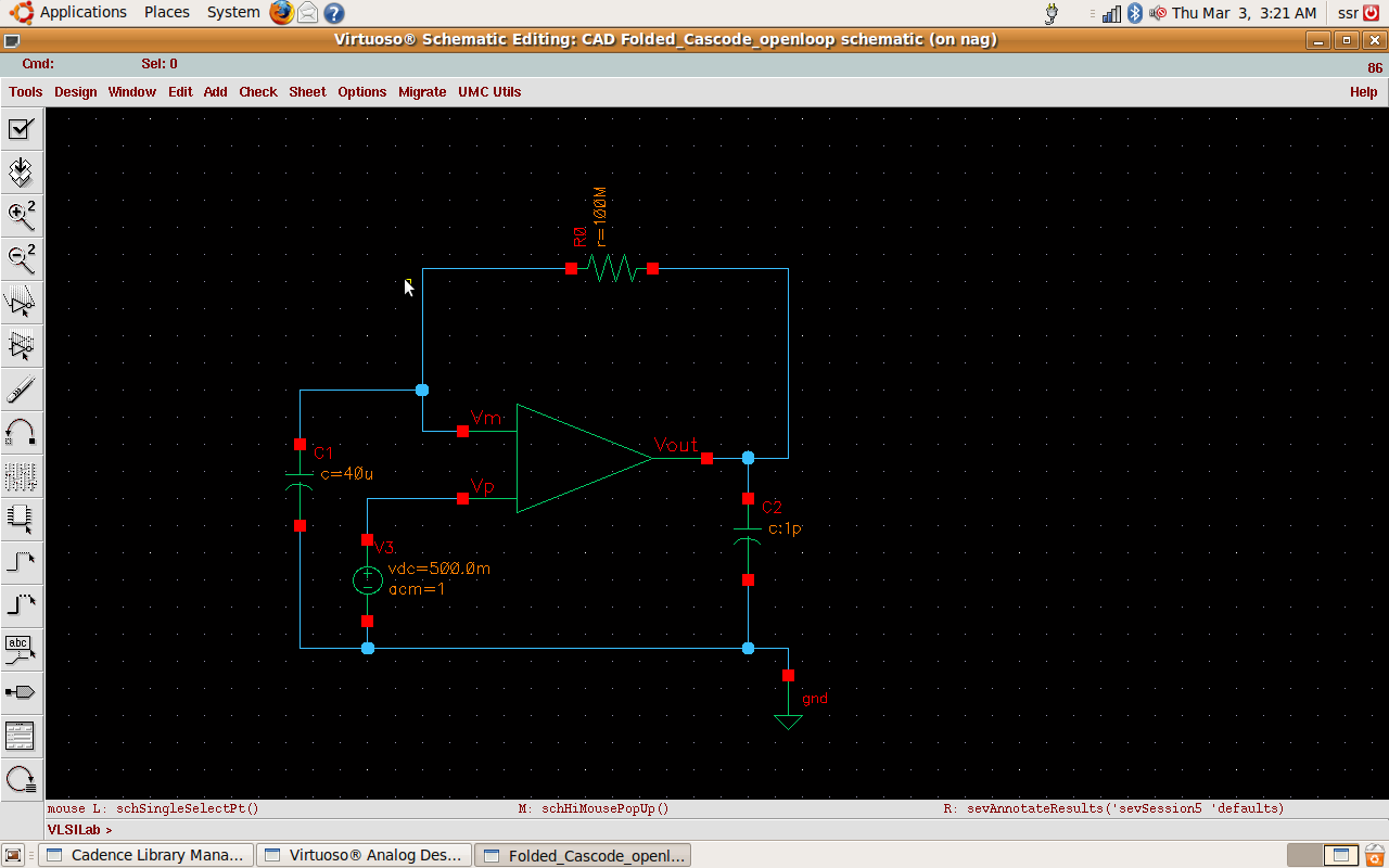
use Fig. 24.39 as a test bench but my output
is oscillating. I don’t understand why. Would you please shed
some
light on what’s going on? Images
of my design and simulation results are seen below (click for a larger
image).
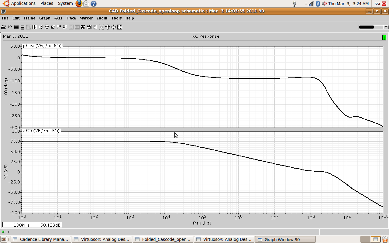
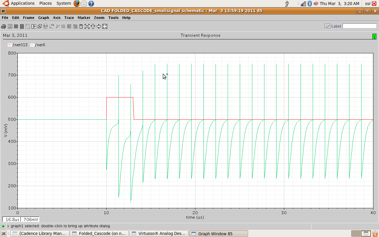
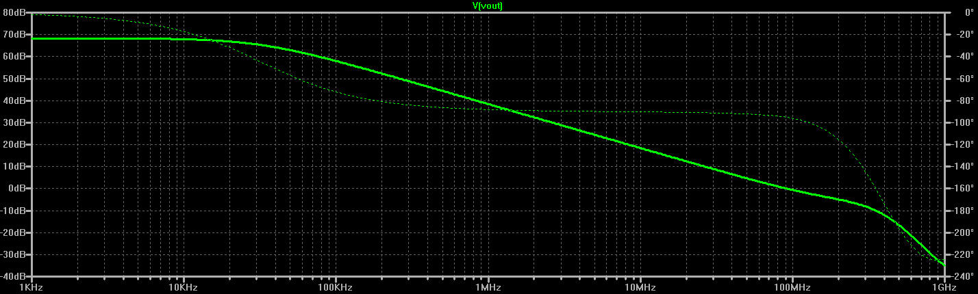
Looks
to me like your phase margin is around
30 degrees, not 54 degrees. This is way too low. Also, you are using
500 mV for
the common-mode
voltage.
While this is the right value,
VDD/2, for the op-amp in Fig. 24.44
since it’s designed in a 50 nm process, I doubt that it’s correct for a
130
nm process. This could lead to the
input diff-pair shutting off and instability.
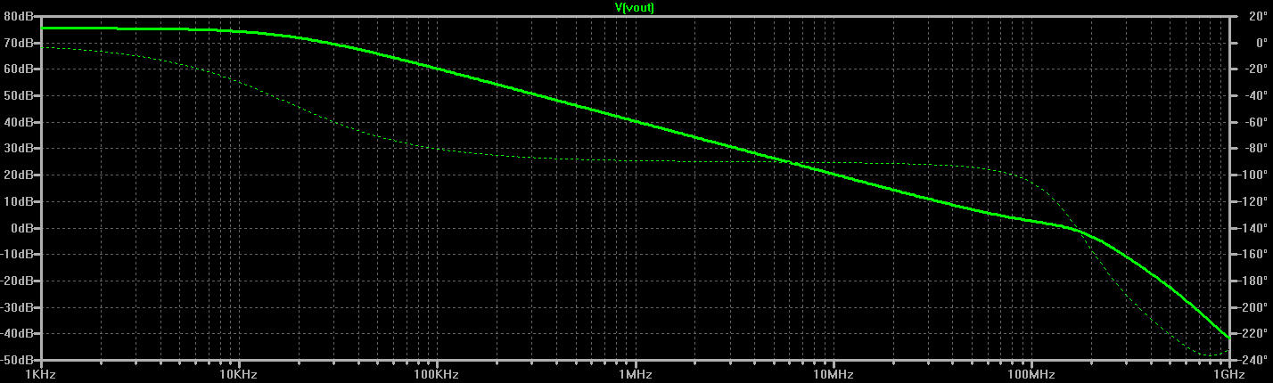
The
phase margin seen in Fig. 24.45 is
about 50 degrees, below.
So,
how do we increase the phase margin
and make the op-amp more stable (and stop the oscillations)? Of course
if we
could reduce the load that would make the design
more
stable but this usually isn’t an
option.
The
answer is that we either increase
the compensation capacitor’s value, Cc,
which lowers the unity-gain frequency, fun,
or we push the pole associated with the output, f2,
out by increasing the
transconductance,
gm2,
of the output stage, see Eq. (24.24).
Since we generally don’t want to slow down the op-amp let’s push out f2. Increasing the
widths of
MON and MOP in Fig. 24.44 by
a
factor of 10 gives the following
results. The unity-gain frequency remains 100 MHz and the phase margin
improves
to roughly 90 degrees. Note that we increase gm2
by increasing the current
in
the output stage (we don’t change
the overdrive voltages of MOP and MON). See comments here
for additional information.