Electric
VLSI Tutorials from CMOSedu.com
Electric
at CMOSedu.com
(examples, downloads, links, etc.)
- Tutorial
1 – Layout and simulation of a resistive voltage divider – electric_tutorial_1_video.mp4 (27:57)
- Tutorial
2 – Layout and simulating the IV curves of PMOS and NMOS
devices – electric_tutorial_2_video.mp4 (33:57)
- Tutorial
3 – Design, layout, and simulation of a CMOS inverter – electric_tutorial_3_video.mp4 (27:45)
- Tutorial
4 – Design, layout, and simulation of a CMOS NAND gate – electric_tutorial_4_video.mp4 (42:25)
- Tutorial
5 – Design, layout, and simulation of a ring oscillator – electric_tutorial_5_video.mp4 (22:41)
- Tutorial
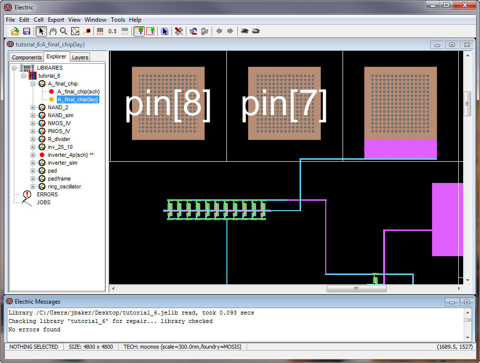
6 – Placing circuit layouts in a padframe
for fabrication – electric_tutorial_6_video.mp4 (33:50)
- Layout of a bandgap
reference – bandgap_video
(69:10) and bandgap.jelib
- PMOS_Body (6:59) – making PMOS body connections, PMOS_divider.jelib and C5_models.txt
- Edit–in–place
(2:58) – very quick introduction to edit–in–place
Below
is tutorial material that was generated with an older version of
Electric that
may still be useful.
Videos introducing
both layout and Electric:
Electric_video_1
(17:42) – drawing a basic inverter schematic, CMOSedu_1.jelib,
inv_20_10.spi,
and inv_20_10.sp
(HSPICE)
(save MOSFET
models, C5_models.txt,
to the C:\Electric directory)
Electric_video_2
(23:38) – more inverter schematic drawing, CMOSedu_2.jelib,
inv_sim_1.spi,
and inv_sim_2.spi
Electric_video_3
(34:55) – layout of an inverter (DRC, ERC, LVS [NCC]), CMOSedu_3.jelib,
Inv_20_10_sch.spi,
inv_sim_lay.spi,
and inv_sim_lay_no_parasitics.spi
Electric_video_4
(15:09) – adding separate connections for power and ground, CMOSedu_4.jelib
and inv_sim_conn_1.spi
Electric_video_5
(09:52) – drawing the schematic of a 21–stage ring oscillator, CMOSedu_5.jelib
and ring_osc_sim_sch.spi
Electric_video_6
(19:06) – lay out of a 21–stage ring oscillator, CMOSedu_6.jelib,
ring_osc_sim_lay.spi,
and ring_osc_sim_lay_with_parasitics.spi
Electric_video_8
(18:30) – lay out a poly1–poly2 capacitor and an RC circuit, CMOSedu_8.jelib,
RC_sim_sch.spi,
and RC_sim_lay.spi
Electric_video_9
(24:25) – drawing the schematic and icon of a NAND gate, CMOSedu_9.jelib,
NAND_2_sch.spi,
and NAND_sim_sch.spi
Electric_video_10
(28:33) – lay out of a NAND gate, CMOSedu_10.jelib
Electric_video_11
(28:15) – drawing the schematic and laying out a NOR gate (no
talking, just
music and the sound of connections!), CMOSedu_11.jelib
Electric_video_12
(10:50) – brief introduction to IRSIM and ALS (asynchronous logic
simulator), CMOSedu_12.jelib
Electric_video_13
(11:33) – brief introduction to using HSPICE
and LTspice
with Electric, CMOSedu_13.jelib
Some
random videos; the jelib
used
in these videos is here.
Electric_4_1
(3:52) – Setting the right scale factor when opening libraries
Electric_4_2
(2:54) – Create new libraries using objects (schematics/layout/icons)
from
other libraries. Moving objects between libraries.
Electric_4_3
(15:33) – How to create and use icons and use them in schematics/SPICE.
Electric_4_4
(4:50) – How to create a new version of a cell
Electric_5_1
(6:04) – Layout of an n–well diode and making an icon view
Electric_5_2
(11:09) – Schematic and simulation of an RC circuit using an n–well
resistor
Electric_5_3
(12:15) – Layout of the metal layers and a pad
Electric_6_1
(2:51) – Layout of a pad that contains metal2 and metal3
Electric_6_2
(2:33) – Layout of a padframe
Electric_6_3
(9:04) – Layout of metal1, metal2 pad and overglass
Electric_7_1
(11:26) – Making substrate connections
Electric_8_1
(10:20) – Layout of an n–well resistor and sizing it for specific
resistance
Electric_8_2
(11:37) – Layout of a poly1 resistor with contacts to a resistor using bondpads
Electric_8_3
(5:28) – Layout of a p+ resistor
Electric_8_4
(2:20) – Layout of NMOS and PMOS transistors
Electric_8_5
(7:26) – Connecting transistors together
Electric_9_1
(15:54) – Schematic and layout of an inverter
Electric_9_2
(5:04) – Layout of an ring oscillator
Electric_9_3
(5:27) – Layout of a long L MOSFET
Electric_10_1
(4:26) – Quick guide to laying out a long–L device without LVS error by
creating an icon
Electric_10_2
(2:13) – How to layout a 4–to–1 divider using four 10k n–well unit
cells
Electric_10_3
(22:26) – Layout of a poly1–poly2 capacitor, icon, an RC circuit
Electric_19_1 (11:50) – 3 terminal and 4 terminal MOSFET symbols, when to use, some SPICE simulations
Return
to:
