Electric
VLSI Design
System
Tutorials
from CMOSedu.com (Return)
Tutorial
5 – Design, layout, and simulation of a ring oscillator
In this tutorial
we’ll design, layout, and simulate the operation of a ring oscillator
using the
setups, and C5 process, from earlier tutorials.
To begin this tutorial, use Electric to open the jelib we created in tutorial 4, tutorial_4.jelib (right click to save to C:\Electric).
Save this library
as tutorial_5.jelib, again in C:\Electric.
Next ensure that
the C5_models.txt are
saved in C:\Electric for SPICE simulations.
One
of the goals of this tutorial is to learn about arrays and buses.
In
this newly saved tutorial_5.jelib library create a schematic view of a
cell
called inverter_4p (4p indicates four inverters in parallel)
In
this cell instantiate 4 inv_20_10 cells as seen below (place the cell 4
times)
You
can go to the arrowhead on the Cell menu item and select/instantiate
this cell
4 times or place it once then use Ctrl+C
and Ctrl+V.
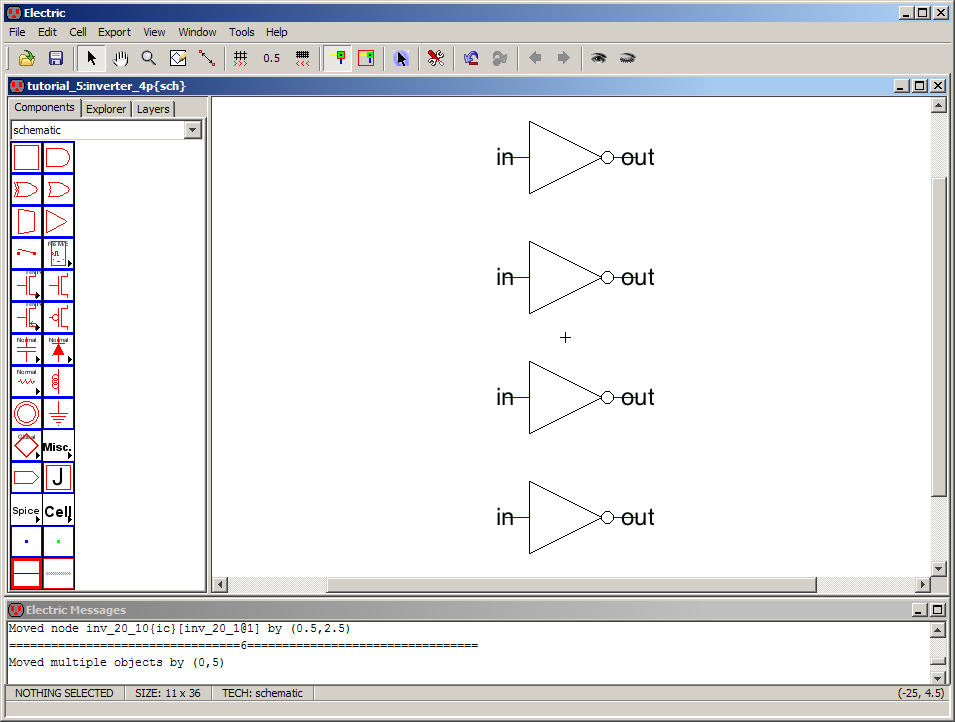
While
this is one way to place inverters in parallel there are other ways
that are
useful.
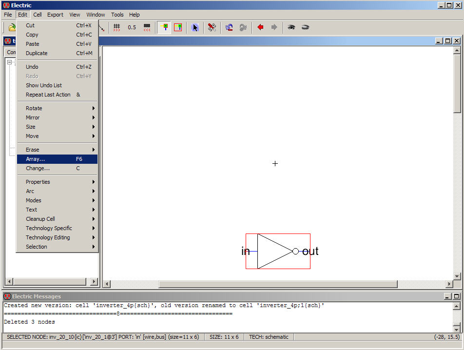
Let’s
Create a New Version of this Cell as seen below.
Note
this is very useful when “trying something out” since the earlier
version is
still present.
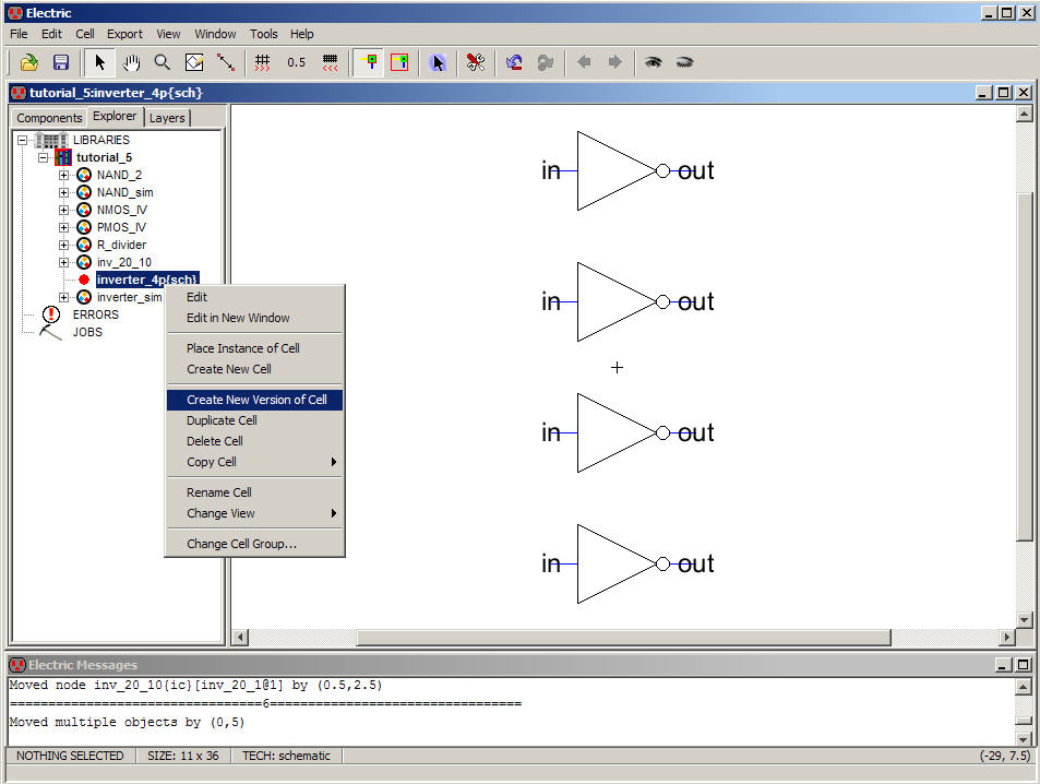
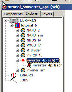
A
screen shot of the Explorer is seen below.
Both
inverter_4p cells contain the same contents right after creation.
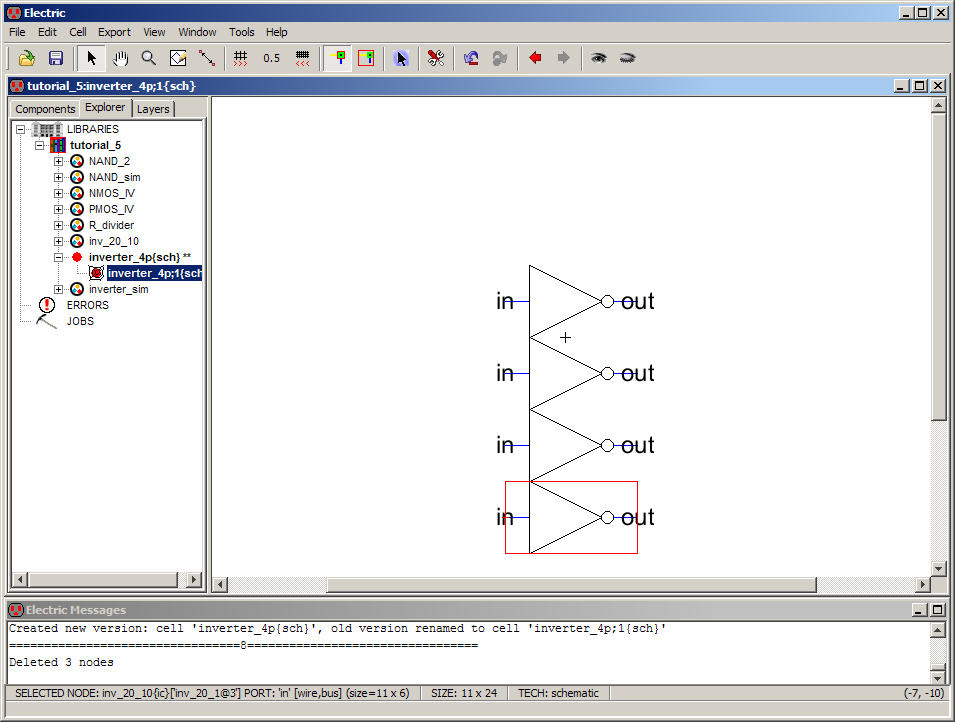
Open
inverter_4p;1 and delete the top 3 inverters as seen below.
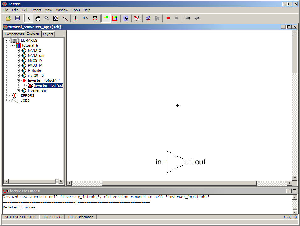
Next
select this inv_20_10 Node (the only thing left in this cell) and the
menu Edit
-> Array (or just press F6).
Set
the X repeat factor to 1 and the Y repeat factor to 4.
Keep
the edge overlaps at 0 as seen below.

And
we get the following.
Since
we didn’t specify an overlap the icons abut
each
other.
Arraying
is most useful in layout, as we’ll see in a moment, since other
“tricks” are
used for schematics.
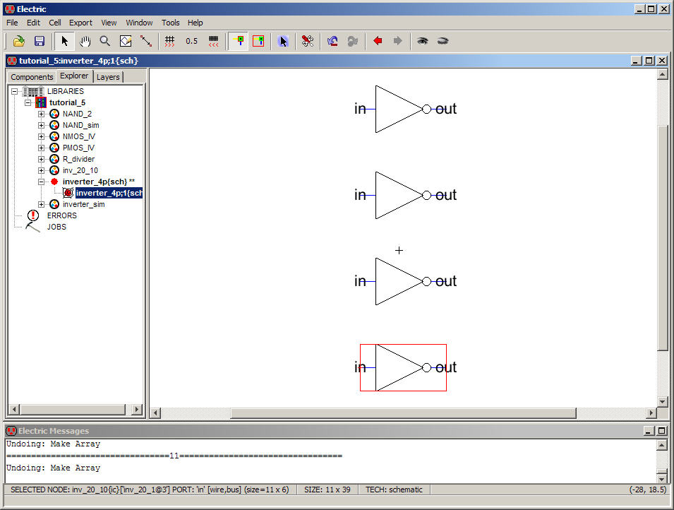
Press
Ctrl+Z to undo the Array
command and go back to the
single inverter.
Press
F6, again with the single icon selected, and set the Y edge overlap to
-5.
Note
that using a negative number indicates that the icons are spaced apart.

The
result is seen below.
As
mentioned a moment ago the Array command (F6) is most useful when doing
layout.
We’ll
use it later in the tutorial when we layout the ring oscillator.
The
concise way of generating the above schematic of 4 inverters in
parallel is to
indicate the array by renaming the icon.
Let’s
demonstrate this now.
Go
to the Explorer and right+click
on the inverter_4p
cell and use the Create New Version of Cell command again.
Since
there are two versions of the inverter_4p cell the contents of the
newly
created cell will be dependent upon (copied from) which cell you right+click on.
It
doesn’t matter at this point since we’ll modify the contents so Create
the New
Version from any view of inverter_4p.
Next
delete three of the inverters Nodes and center the remaining inverter
Node
around the origin as seen below.
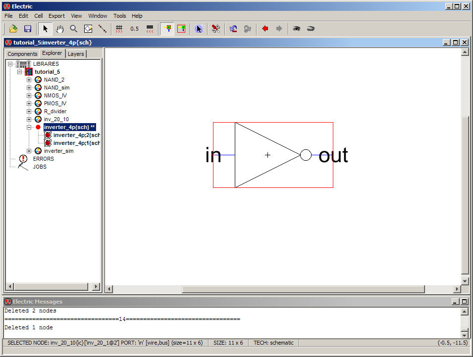
Next
Edit the object’s properties (Ctrl+I)
and change the
name to something ending in [0:3] (indicating 4 icons).
Below
is an example.
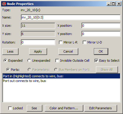
Hitting
OK we get the following.
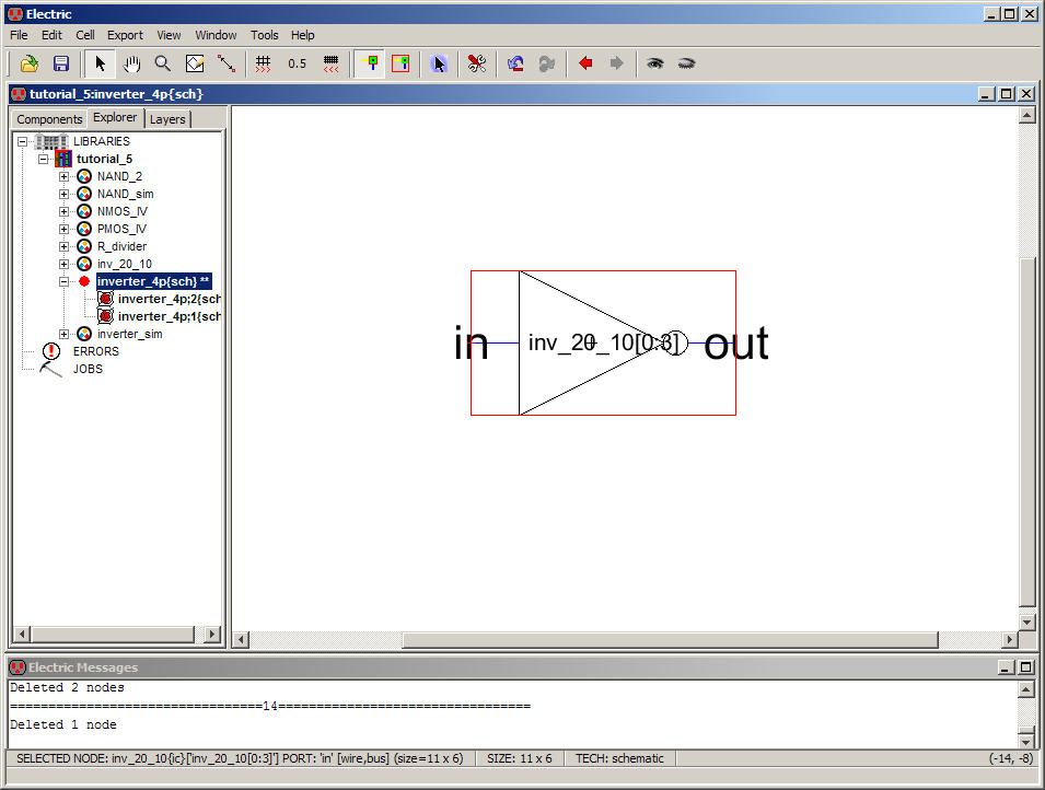
This
schematic is equivalent to placing 4 inverters icons in the cell.
Use
Ctrl+click to select and
move the icon’s name as seen
below.
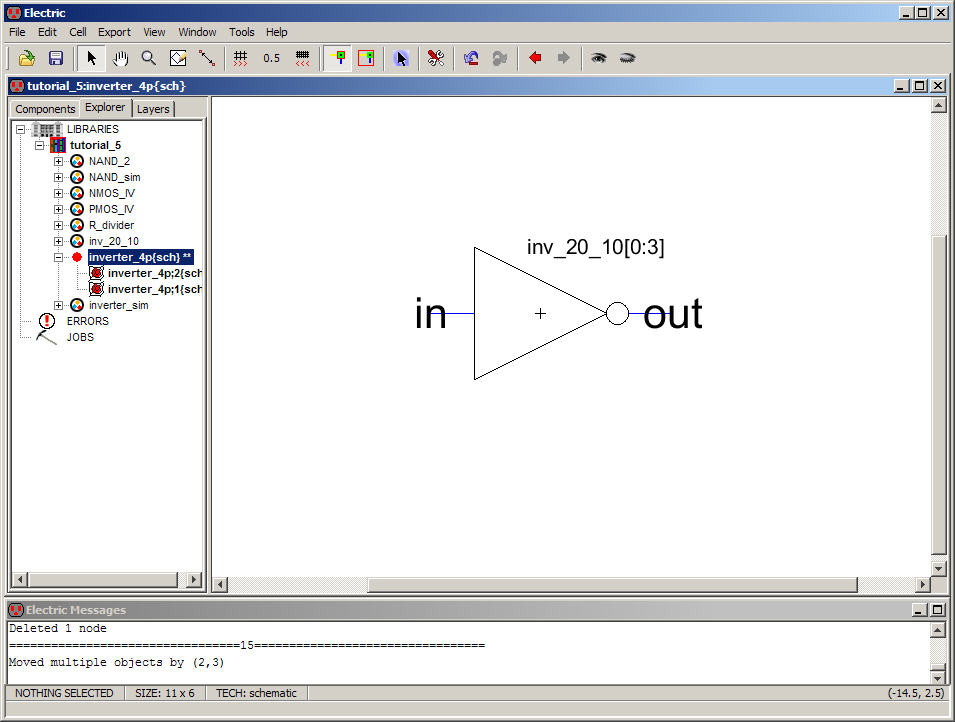
The
next question is “How do we connect wires to these icons?”
If
we connect a wire Arc to the input, as seen below, then all 4 inverter
inputs
are shorted together.
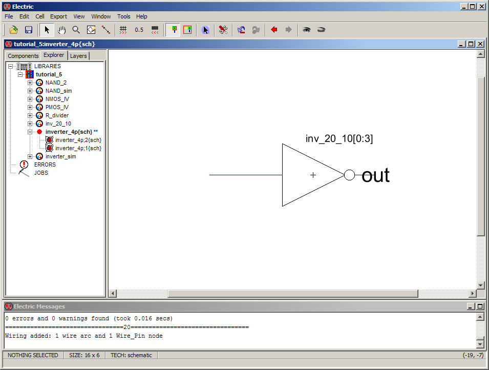
This
may or may not be desirable.
Perhaps
it’s undesirable and we want to have access to each inverters input. In
this
case we can use a bus Arc.
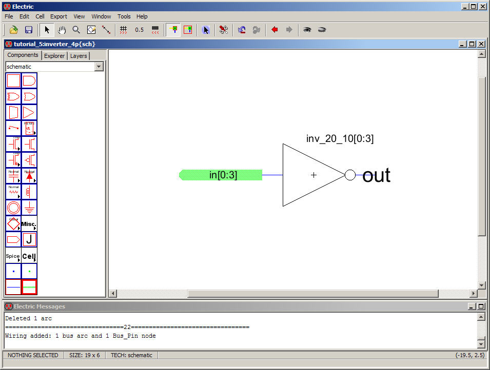
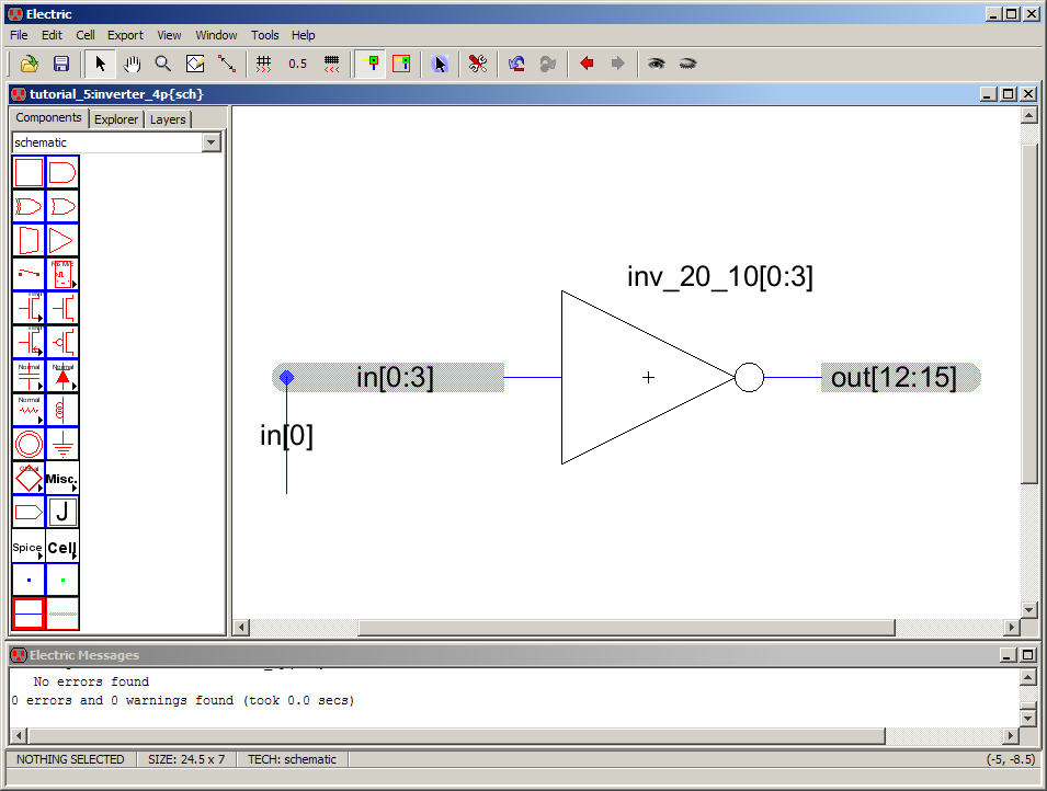
Let’s
name the bus in[0:3] using Edit -> Properties -> Object
Properties (Ctrl+I)
so
that in[0] corresponds to the input of inv_20_10[0], in[1] to
inv_20_10[1] etc.
Let’s
connect the outputs of the inverters to a bus too but let’s do this a
little
differently.
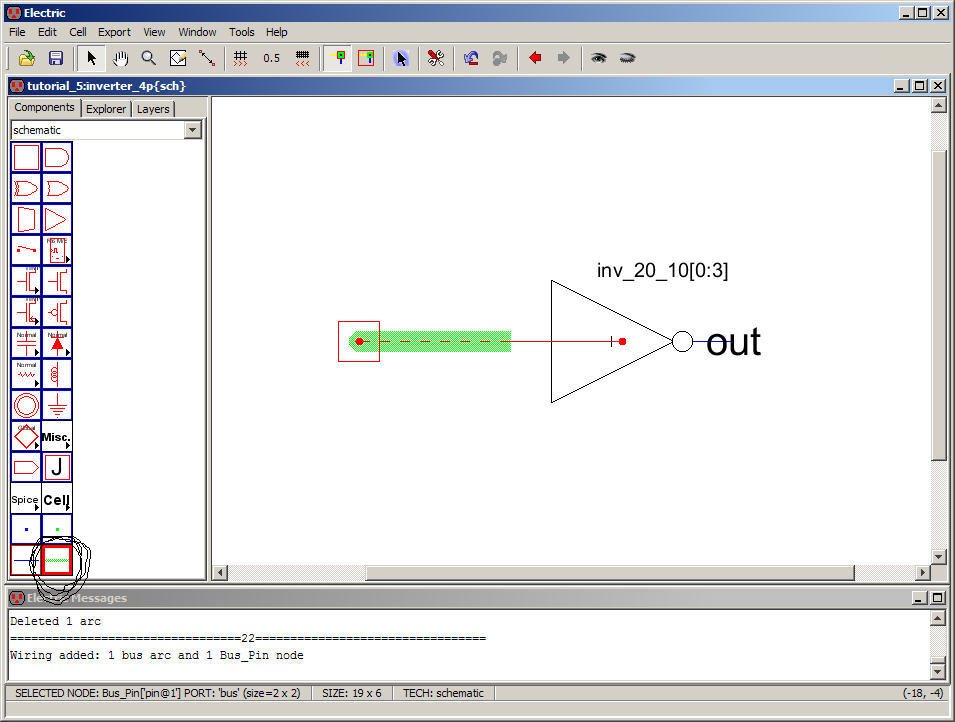
Select
the Bus Pin and place as seen below.
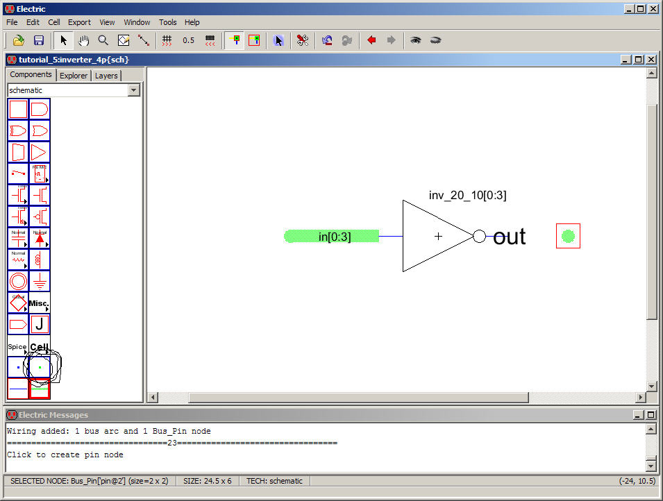
Next,
with the Bus Pin active, right+click
on the output of the inverter icon to connect the bus to the four icons.
Name
the bus out[12:15] as seen below (some arbitrary name
that is 4 long).
Check
your schematic (by pressing F5).
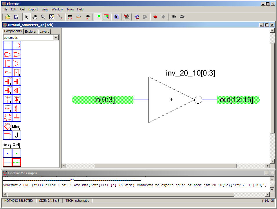
inv_20_10[0]’s
input is in[0] and its output is out[12] and,
as another example,
inv_20_10[3]’s
input is in[3] and its output is out[15]
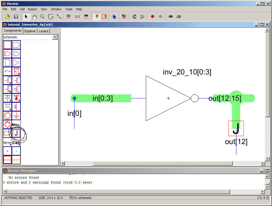
The
next question we need to answer is how do we connect a
wire to the bus?
This
connection can be done by connecting the wire to a Bus
Pin, below
Note
that the schematic doesn’t check (F5) without errors
unless we specify the name of the wire Arc.
The
other way to connect a wire to a bus is to use the Wire
Con Node as seen below.
We
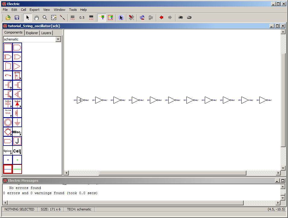
are now ready to draw the ring oscillator schematic.
Create
the schematic view of a cell called ring_oscillator
and place an inverter in the cell.
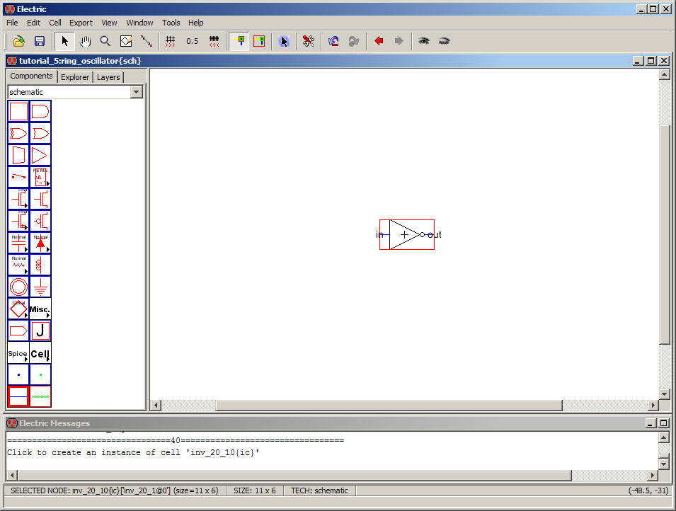
Next
use Cell -> Array (or press F6) with the following
parameters (11-stage ring oscillator)
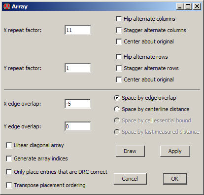
Generating,
after filling the window, the following display.
Next
we need to wire the circuit together.
We
could do this for each stage or turn on the Enable
Mimic-Stitch feature.
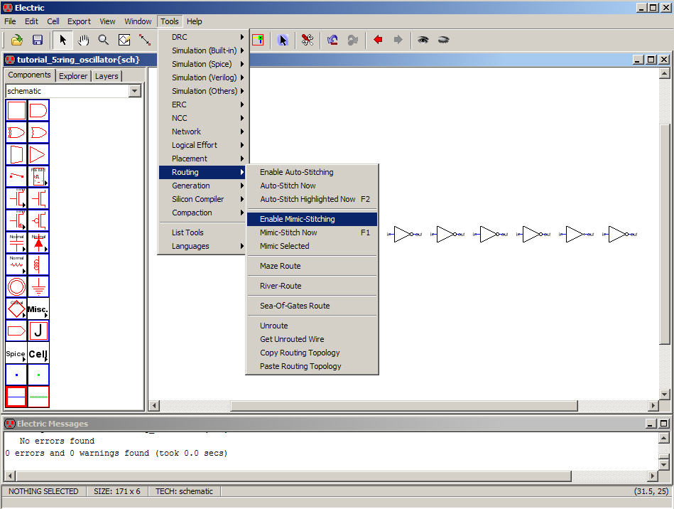
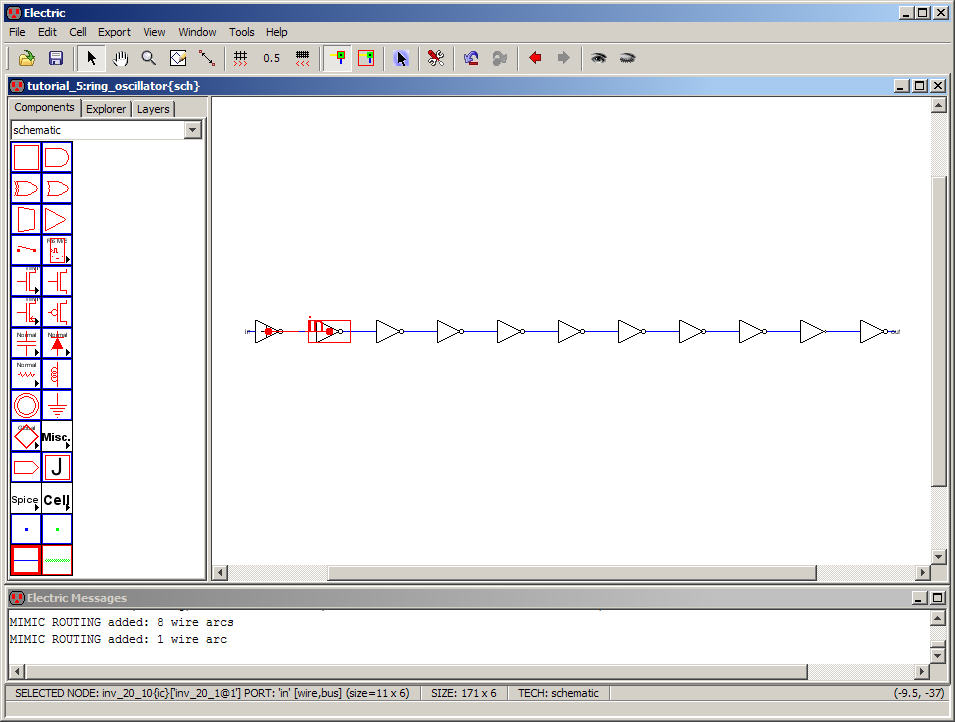
Wiring
the left two inverters together results in the
following.
It’s
very important to go back and turn this feature off
(else unwanted behavior may occur which is a big problem if you forget
this
feature is on ;-)
Disable
the Mimic Stitching now (use the same menu items as
used to enable mimic stitching above).
Add
the last wire Arc and label it osc_out
(and change its text size to 5) as seen below.
Next
add the Spice code, seen below, and change its size to
5.
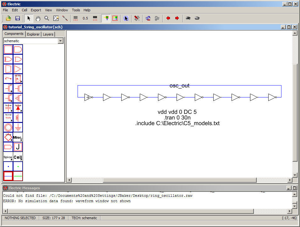
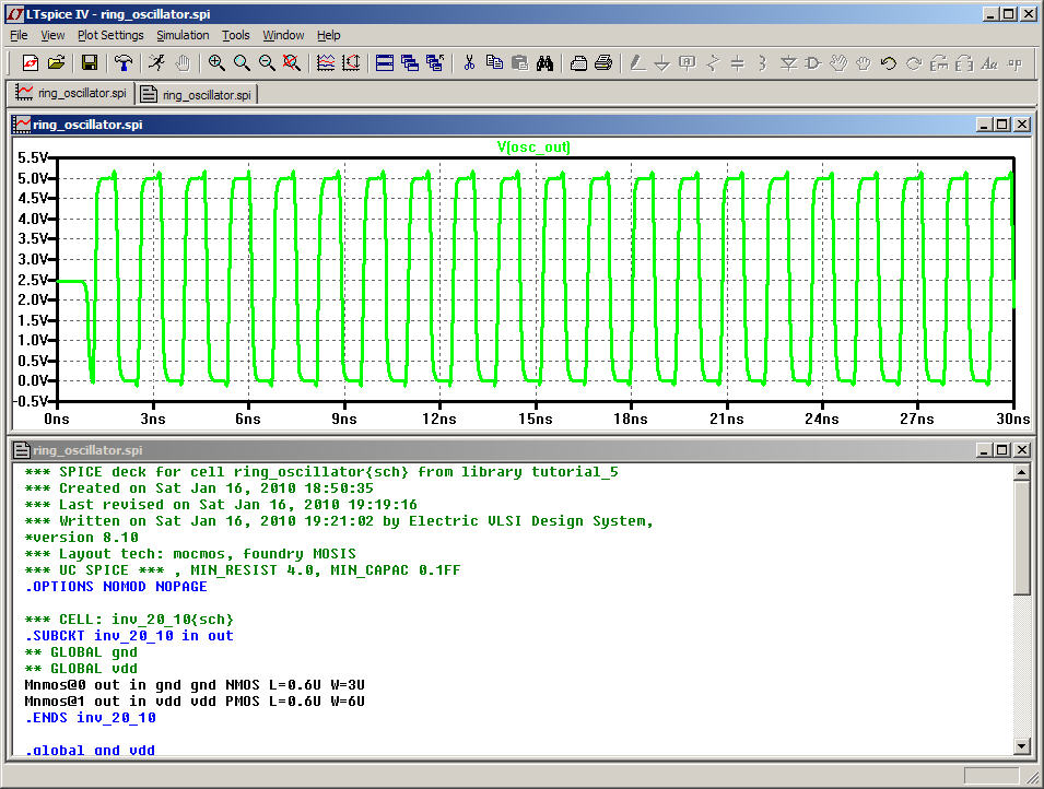
Simulating
this circuit with LTspice gives the following.
If
the circuit doesn’t oscillate add a UIC to the end of the
.tran statement, .tran 0 3n
UIC to “use initial conditions” (set all nodes to zero volts to start)
Using
Electric’s waveform we get the following.
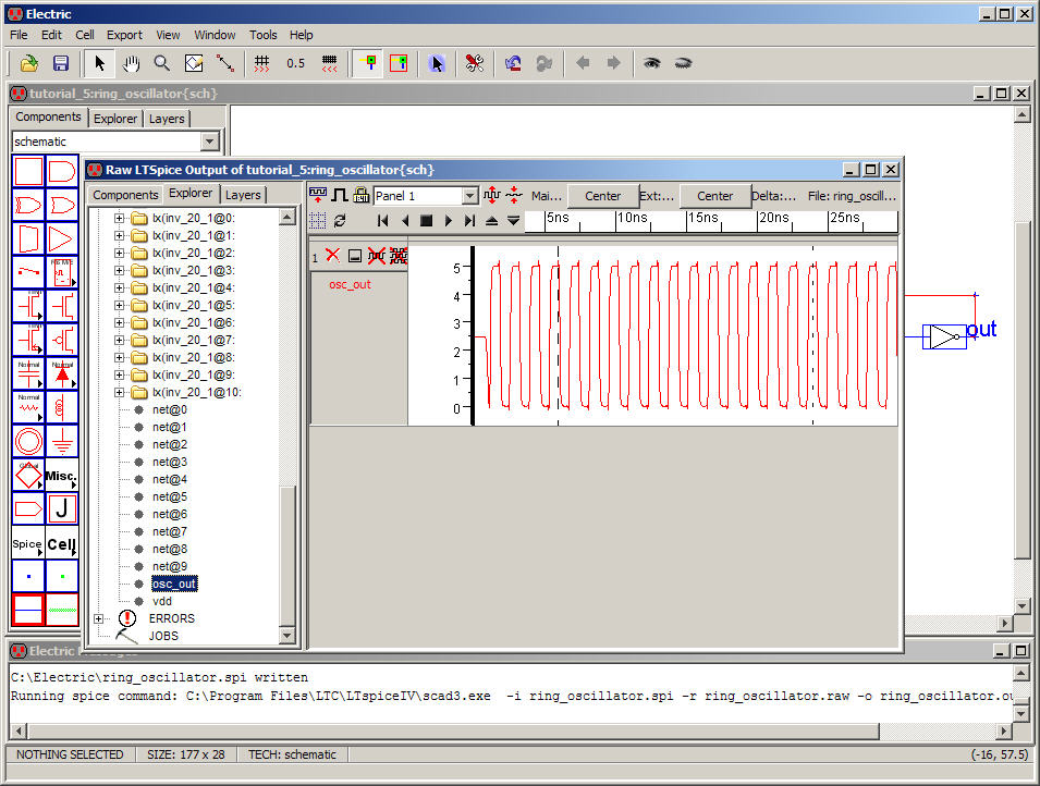
Note,
in the above ring oscillator schematic, the input of
the first inverter and the output of the last inverter is osc_out.
Make
a new version of the ring oscillator cell.
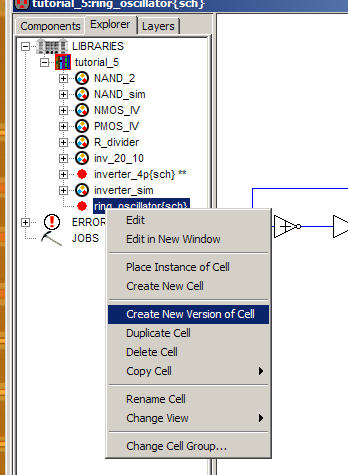
In
this version delete all inverter icons but one and change
the Spice code text size from 5 to 2.
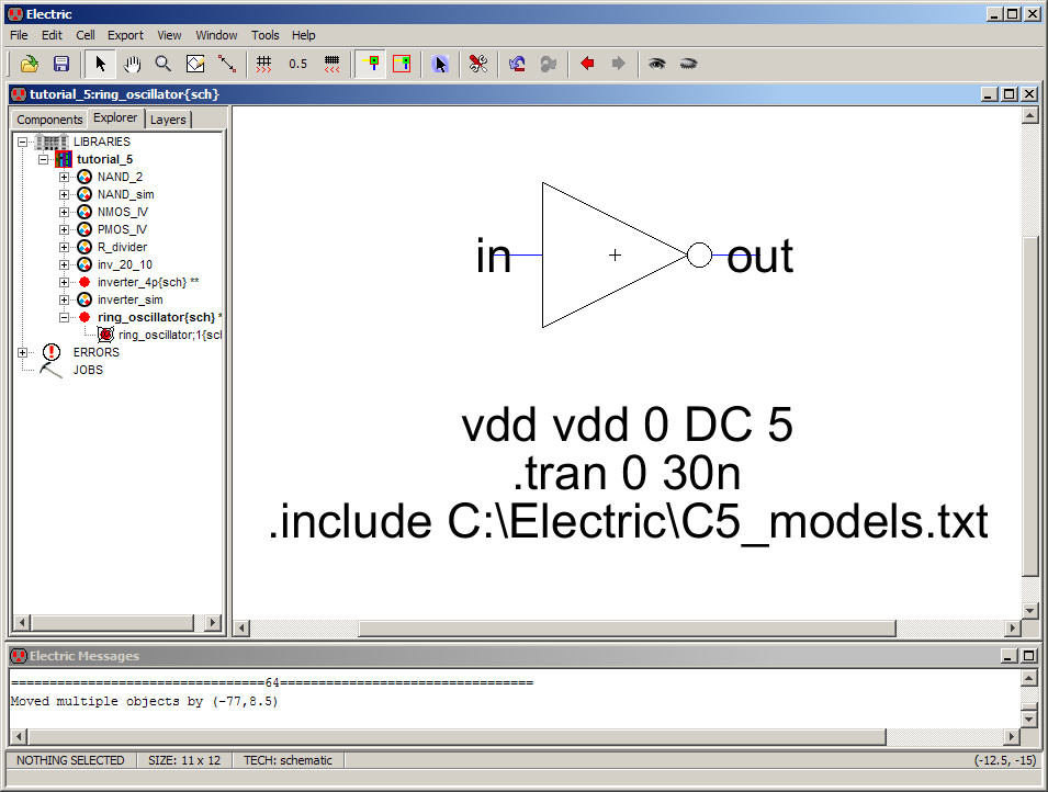
Change
the icon’s name so that it’s inverter[0:10] and
reposition.
Next
add buses to the input and output.
Finally,
name the bus Arcs as seen below.
inverter[0]’s
input is osc_out and
its output is out[0]
inverter[1]’s
input is out[0] and its output is out[1]
inverter[10]’s
input is out[9] and its output is osc_out
This
schematic is equivalent to the ring oscillator seen
above but, obviously, much more concise.
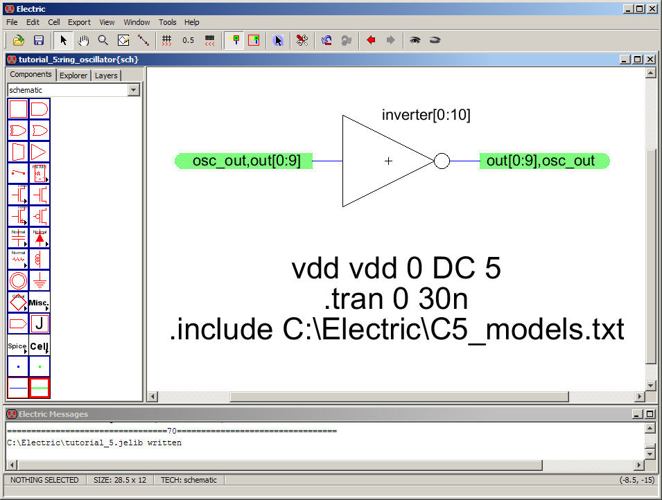
Go
ahead and simulate this circuit.
Next
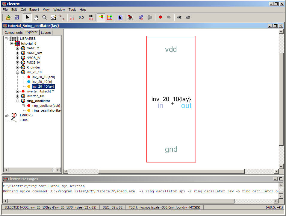
let’s layout this ring oscillator.
Make
a layout view of the ring oscillator and place the
layout of the inv_20_10 in this new cell.
With
this cell selected use F6 (the Array command) with the
following parameters.

The
result, after filling the window, is the following.
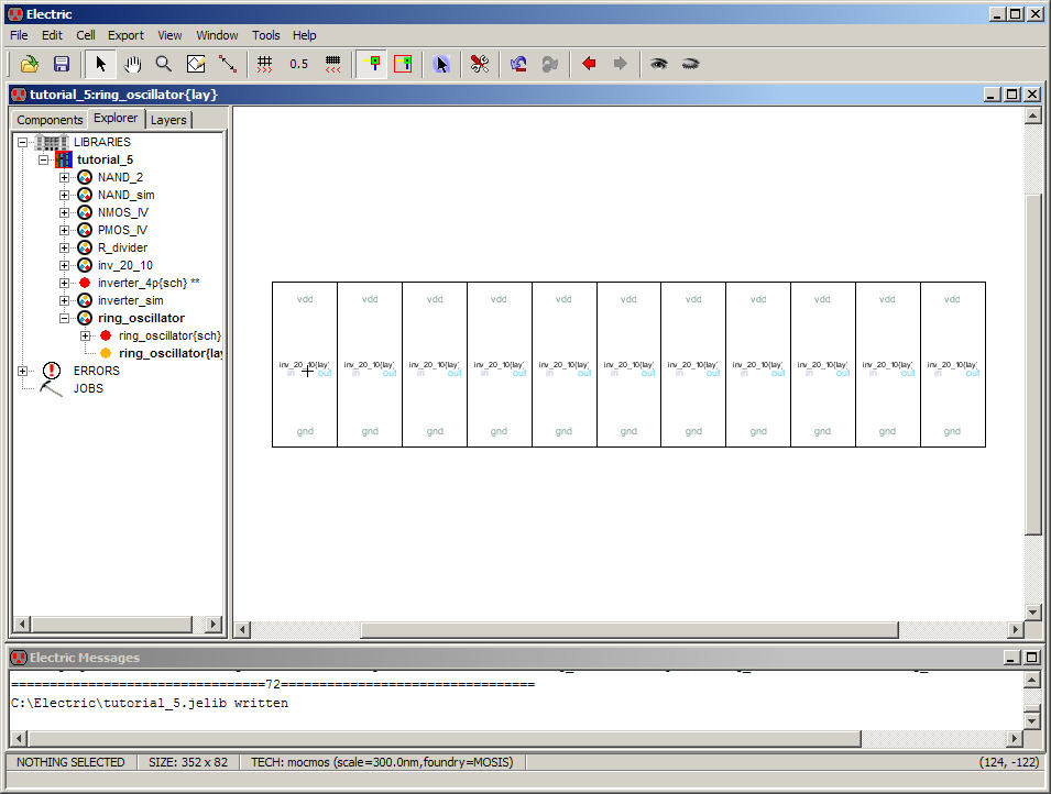
DRC
the layout to see that there aren’t errors.
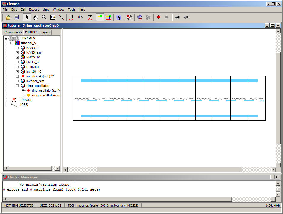
Next
connect adjacent vdd, gnd, and in/out to get the
following.
DRC
the layout.
Next
add metal1-metal2 Nodes at the ends as seen below.
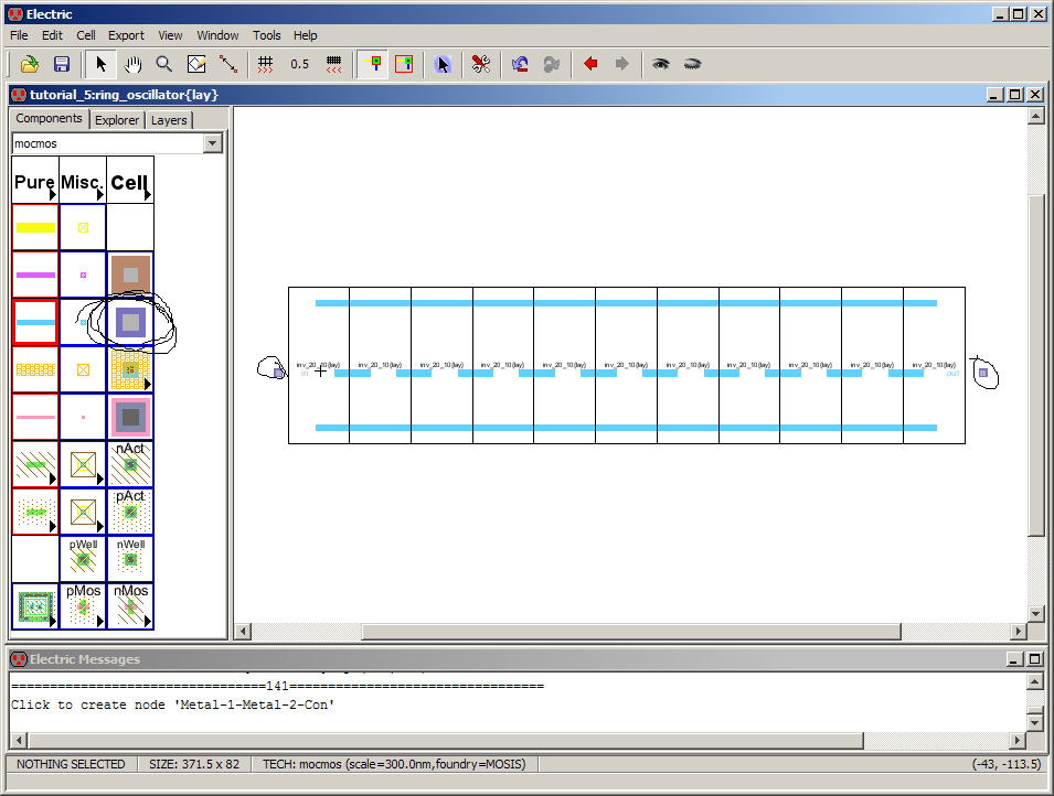
Use
the metal1 Arc to connect the metal1-metal2 Nodes up to
the input and output of the string of inverters as seen below.
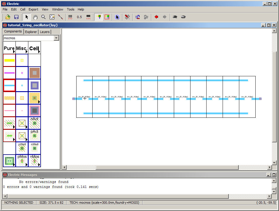
Next
select the metal2 Arc from the menu and connect the
output of the inverter string back around to the input.
Name
this metal2 Arc osc_out
and
change its size to 10 (using Ctrl+click
is useful to
cycle through the selections).
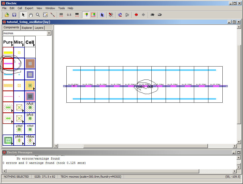
DRC
your design to ensure there aren’t errors.
Finally,
we need to export vdd
and
gnd.
Select
the top metal1 connection on right-most inverter and
export vdd (see below).
Repeat,
using the bottom metal1 connection to export gnd.
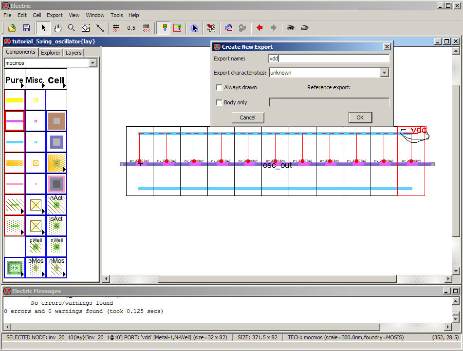
Add
the Spice code from the schematic views.
Change
the text size of the Spice Code and the vdd
and gnd Exports to 10.
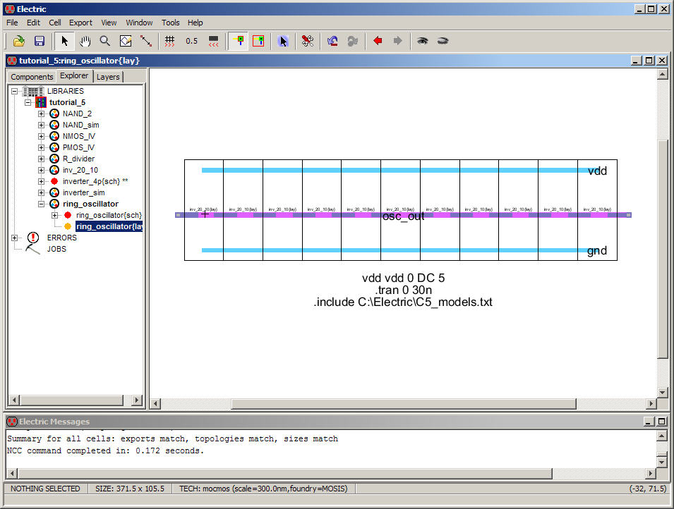
At
this point the layout and schematics match (verify with
NCC), DRC and Well Check correctly.
Select
everything in this cell and press the open eye on the
right top of the menu to see the entire layout.
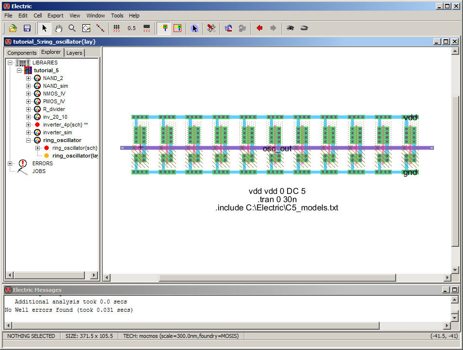
Let’s
simulate the operation of this cell before quitting.
Using
the Preferences -> Tools -> Spice Parasitics we
can simulate using transistor source/drain areas (only) or using models
of the
wires (poly, metals).
In
any case we expect the oscillation frequency of the ring
oscillator to be lower than the simulated value from the schematic
because of
these parasitics.
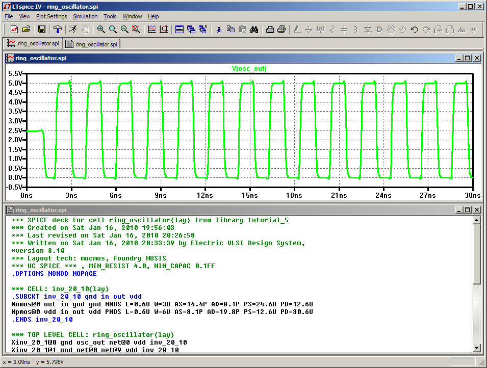
Below
is the LTspice simulation results for the layout
(compare with the schematic simulation results seen above).
Save
the library.
This
is the end of the fifth tutorial.
For
your reference the final jelib
used in this tutorial
is located in tutorial_5.jelib