Electric
VLSI Design
System
Tutorials
from CMOSedu.com (Return)
Tutorial
4 – Design, layout, and simulation of a CMOS NAND gate
In this tutorial
we’ll layout and simulate the operation of a CMOS NAND gate using the
setups,
and C5 process, from Tutorial 1.
To begin, use Electric to open the jelib we created in tutorial 3, tutorial_3.jelib (right click to save to C:\Electric).
Save this library
as tutorial_4.jelib, again in C:\Electric.
Next ensure that
the C5_models.txt are
saved in C:\Electric for SPICE simulations.
Next
right click on the cell group inv_20_10 and select Duplicate Cells in
Group as
seen below.
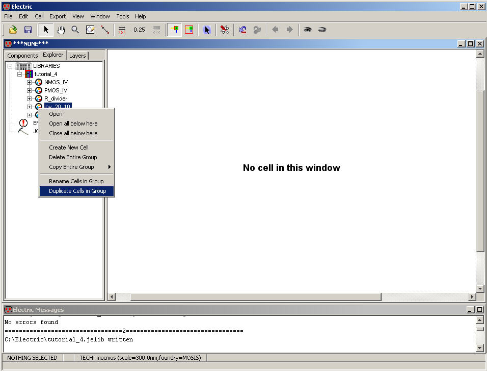
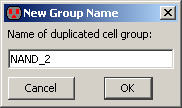
Name
the new cell group NAND_2 (where the 2 indicates two
inputs).
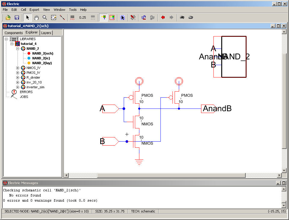
Open
the schematic view of this cell and delete the wire
Arcs, Off-Page Nodes, and the icon view.
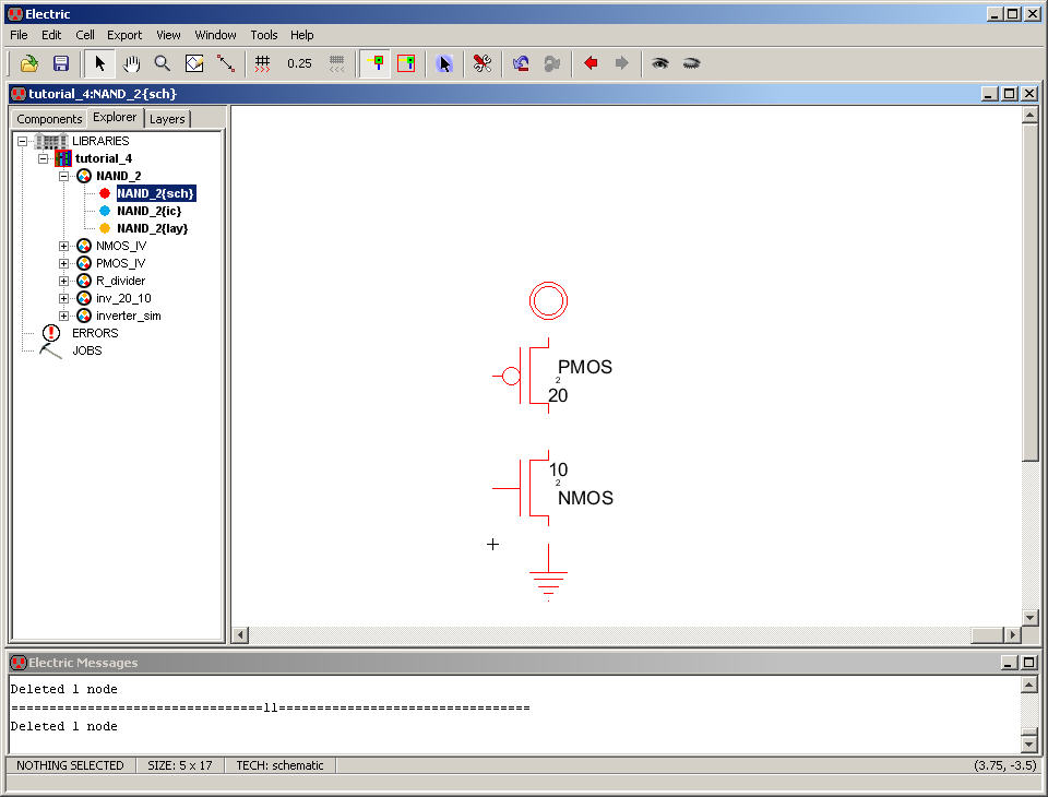
Change
the width of the PMOS from 20 to 10.
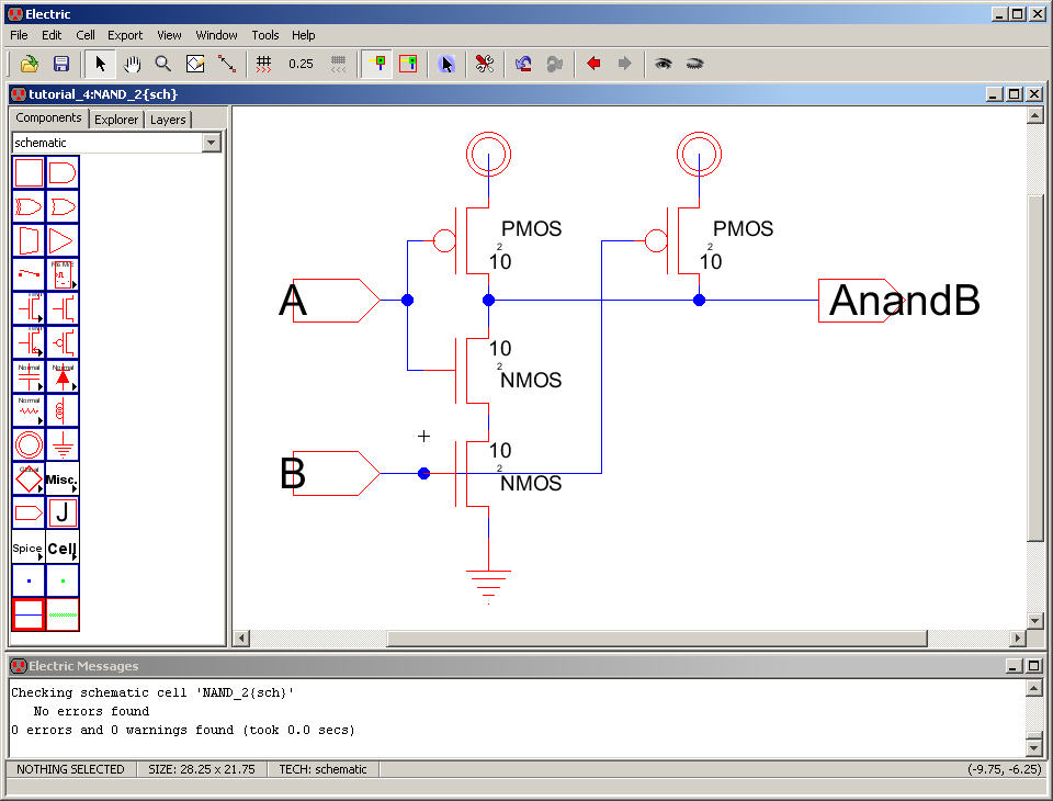
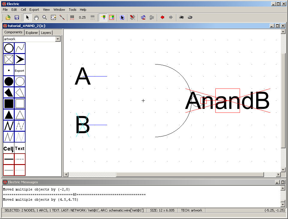
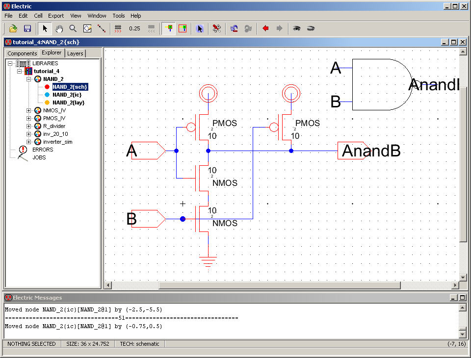
Copy
the PMOS and NMOS Nodes then wire the NAND gate together
as seen below.
Make
sure to Export the off-page nodes as seen below (note
that if you don’t understand how to do this then go back through Tutorial
3)
Get
into the habit of checking your schematics, F5, and using
Edit -> Cleanup Cell -> Cleanup Pins Everywhere (I bound
the F4 key to
this command, see Tutorial
1 for information on key bindings)
Delete
the icon view of this cell using the Explorer.
Then
use View -> Make Icon View to make a new icon view.
Remember
that this view will be instantiated in the schematic
as seen below.
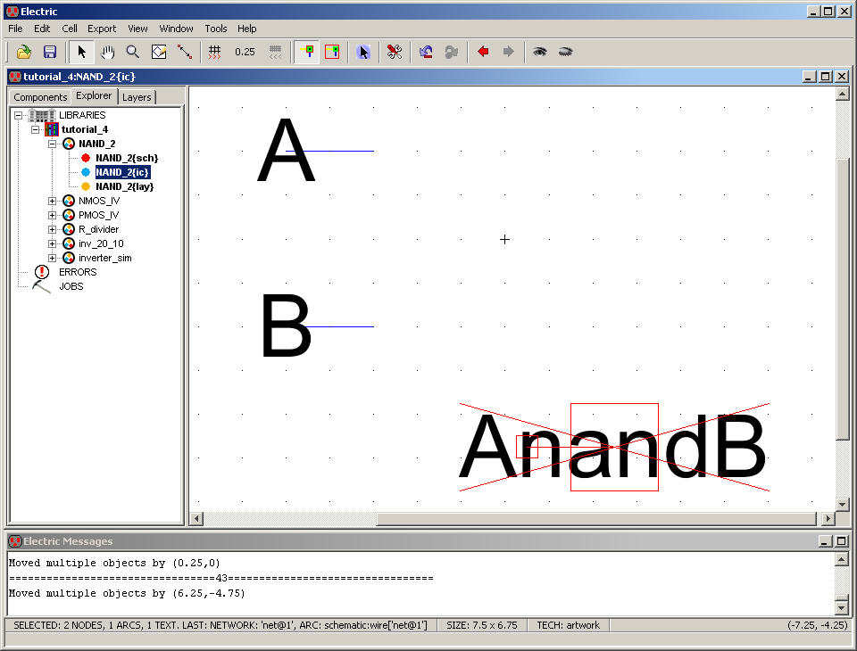
Go
into the icon view and delete the box.
Show
the grid (Ctrl+G).
Rotate
and move the AnandB
Pin/Arc
as seen below.
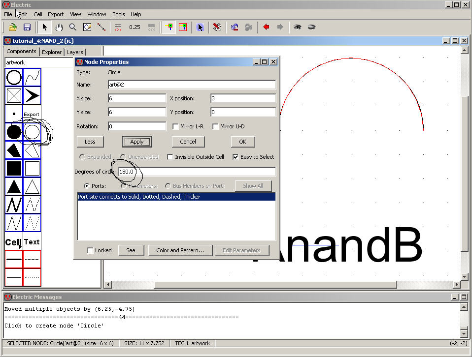
Next
add a circle and change its properties so that “Degrees
of circle” is 180 as seen below.
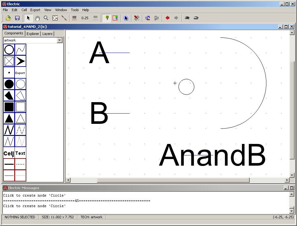
Rotate
this semicircle and add another circle.
Change
this added circle so that both its x and y sizes are
1.
Move
the objects to start forming the icon of the NAND gate.
Next
add the Opened-Polygon Node to the icon.
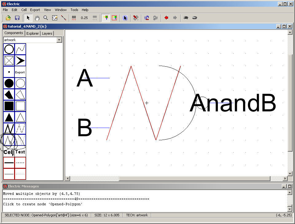
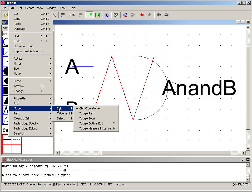
With
the Node selected use Edit -> Modes -> Edit ->
Toggle Outline Edit (or just press Y) to change the shape of the Node.
This
one is very important and perhaps a little hard to
remember until you’ve used it a few dozen times.
When
in this mode the mouse pointer changes to a pencil.
To
add a vertex to the Polygon right click the mouse button
in the same manner as adding to an Arc.
To
exit press Y again or use the menu Edit -> Modes ->
Edit -> Toggle Outline Edit.
Adjust
the shape of the polygon until it looks like the
following.
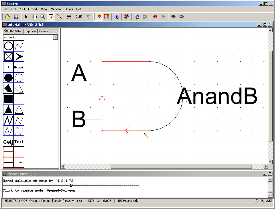
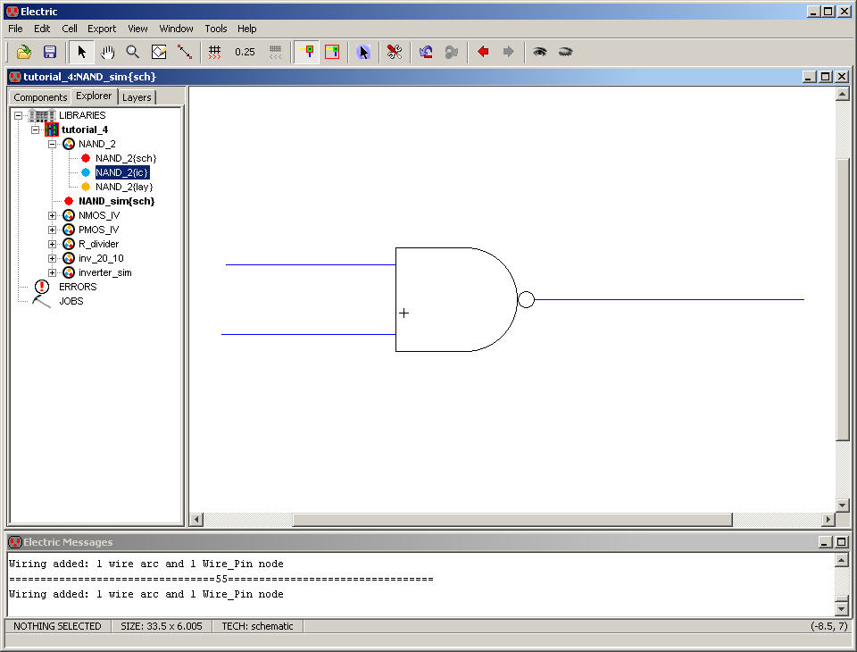
Go
back to schematic view and move the instantiation of the
icon until the contents of the cell look similar to the following.
Turn
off the grid and save the library.
Before
moving on to the layout let’s simulate the operation
of this NAND gate.
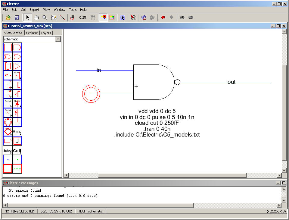
Make
schematic view of a cell called NAND_sim
Place
the NAND_2 icon into this cell and connect Arcs to the
inputs and output as seen below.
Label
the Arcs and add Spice Code and power as seen below.
Spice
code is found under the arrowhead on the Misc. menu
item.
Make
sure to check your design, F5.
Use
Tools -> Simulation (Spice) -> Write Spice Deck to
run an LTspice simulation.
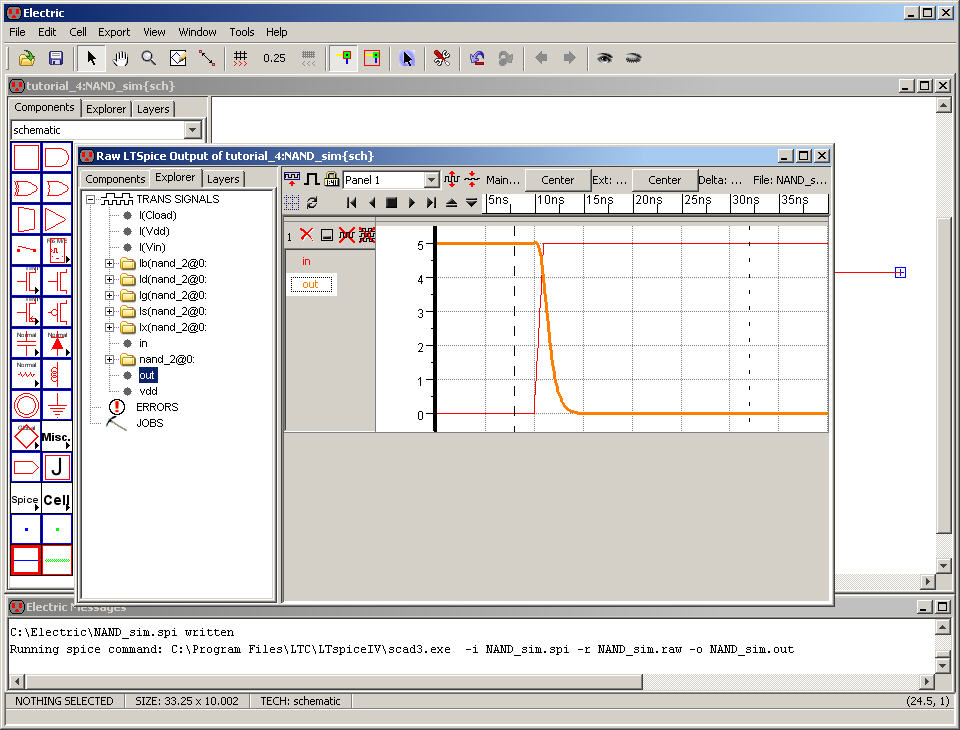
Plot
the input and output signals using LTspice as seen
below.
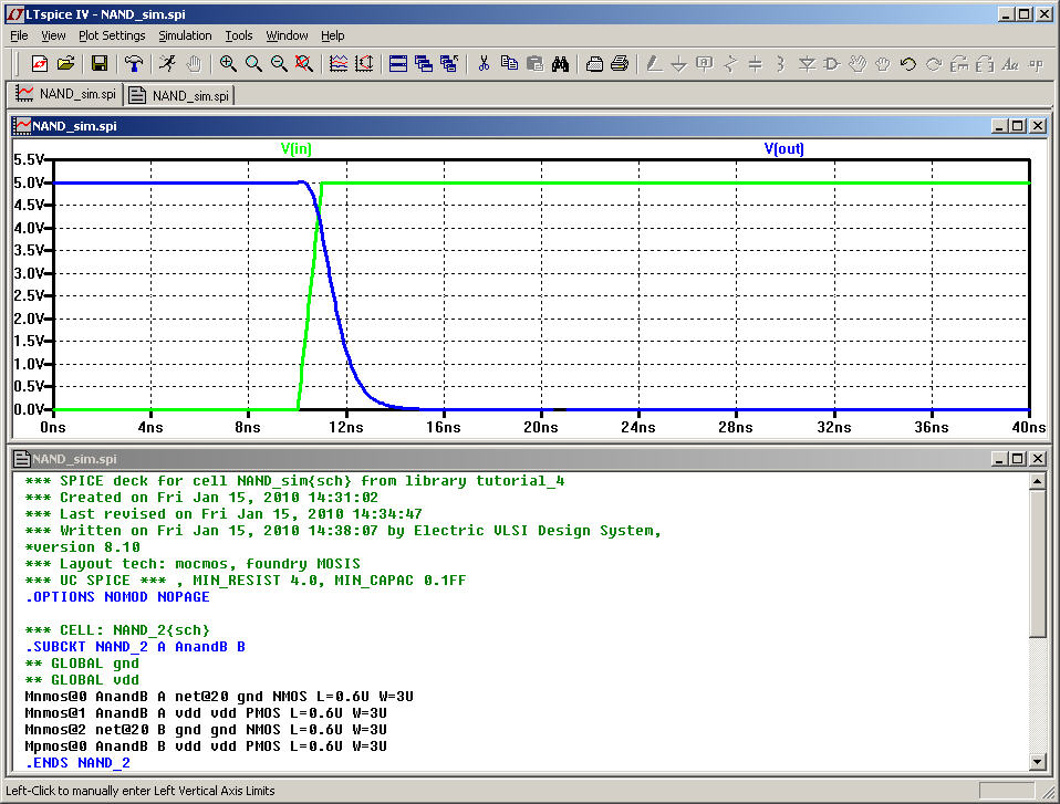
Closing
LTspice (and ensuring via LTspice’s
Tools -> Control Panel -> Operation that the raw files
are not
automatically deleted) allows us to use Electric’s waveform viewer.
Let’s
move on to laying out the NAND gate.
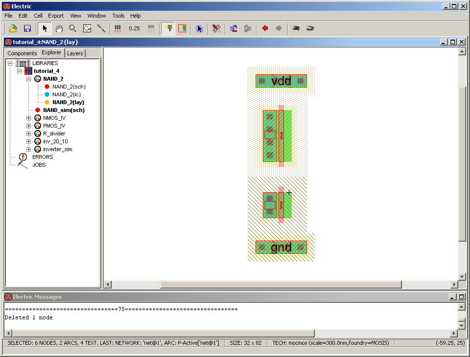
Open
the layout view of the NAND_2 cell.
This
cell contains the layout of the inverter we did in
Tutorial 3.
Delete
the Arcs, Pins, and Exports until you get the
following.
Next
move the pAct and nAct Nodes away from the
transistor Nodes as seen below.
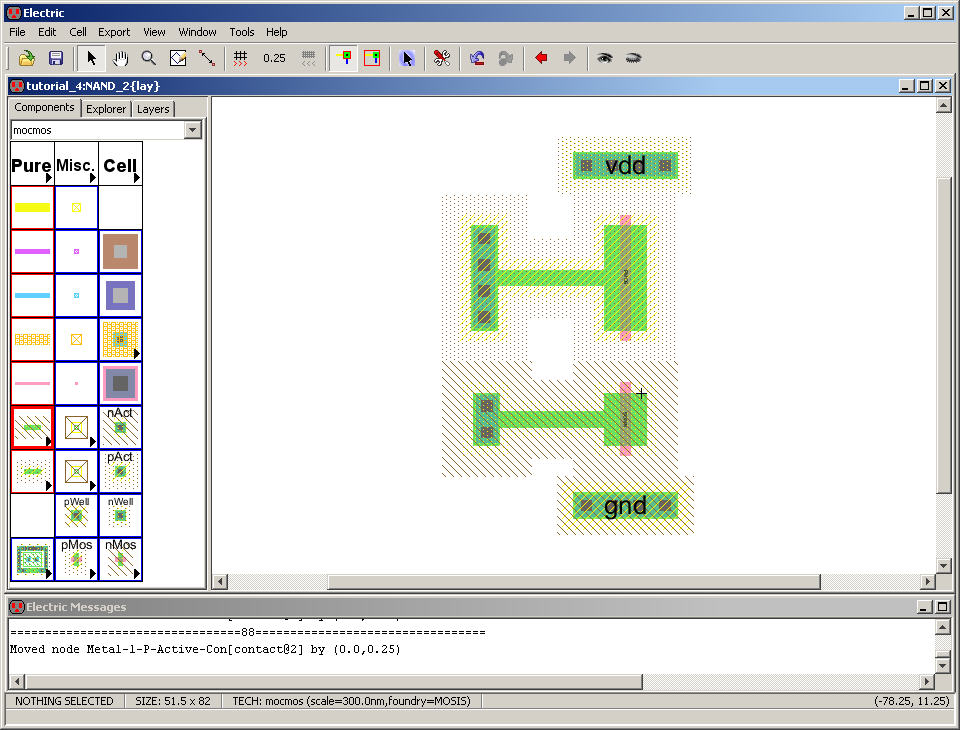
Change
the width of the pMos
Node
and the y-size of the pAct
Node to 10.
Copy
the pAct Node twice,
the pMos Node once, the
nAct Node
once, and the nMos Node
once and place as seen below.
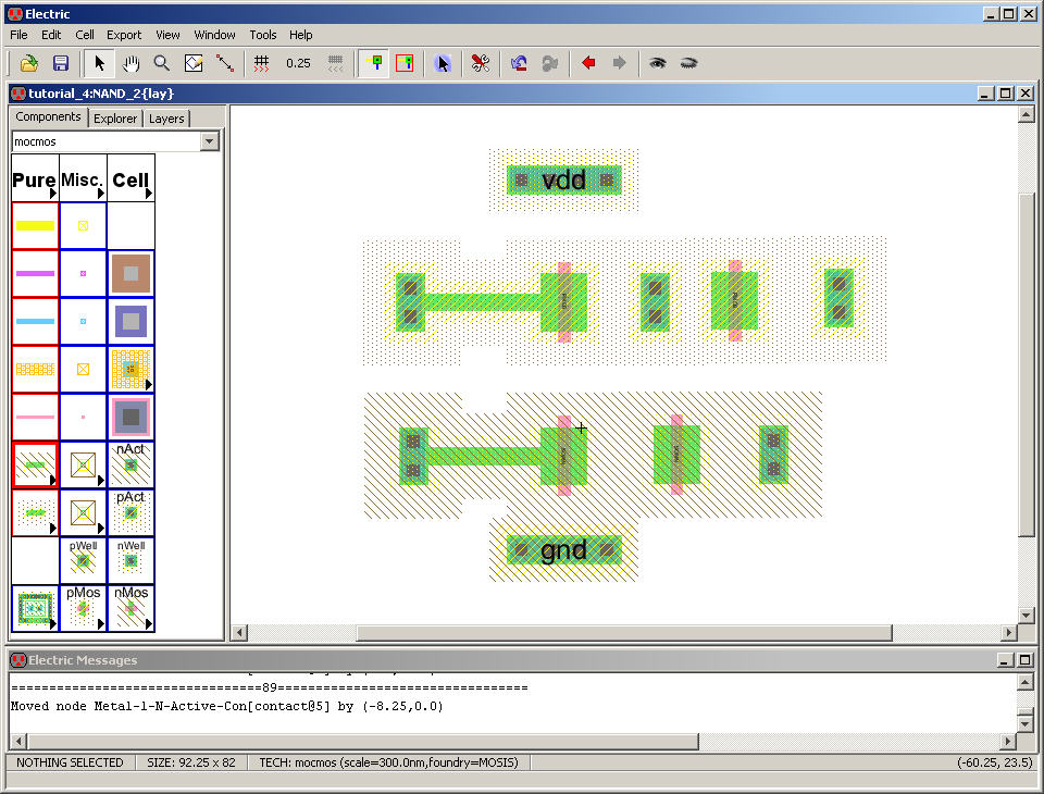
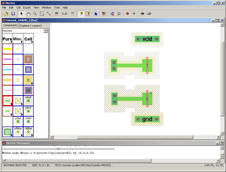
Next
add Arcs as seen below.
Next
move the Nodes together.
DRC
the layout to ensure no errors.
Increase
the x-size of the pWell
and nWell nodes to 30.
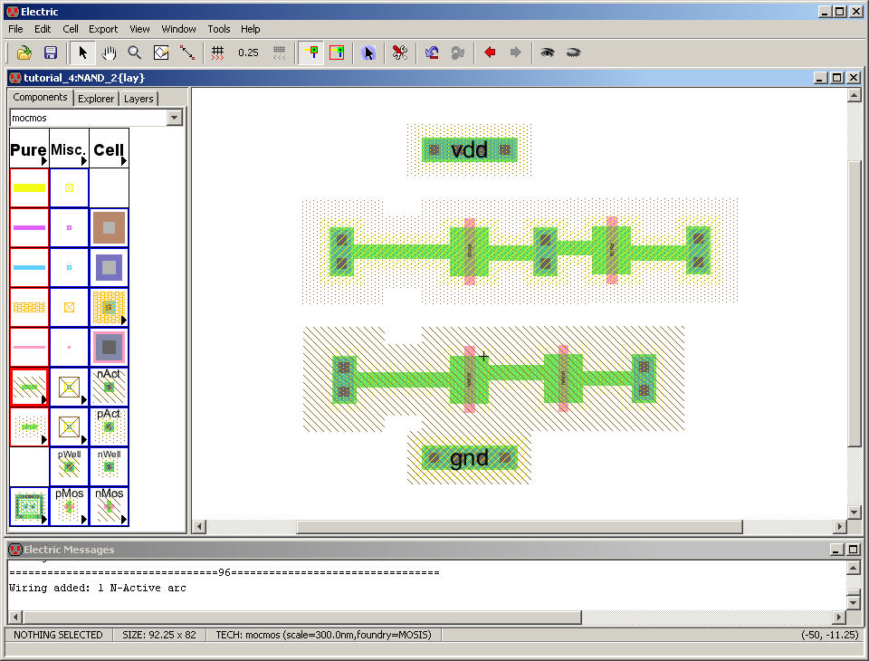
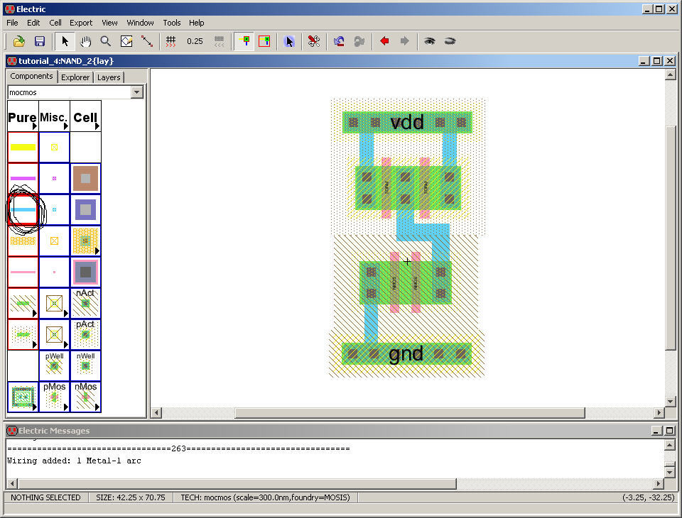
Connect
metal1 Arcs as seen below.
Ensure
that the metal1 Arc is selected.
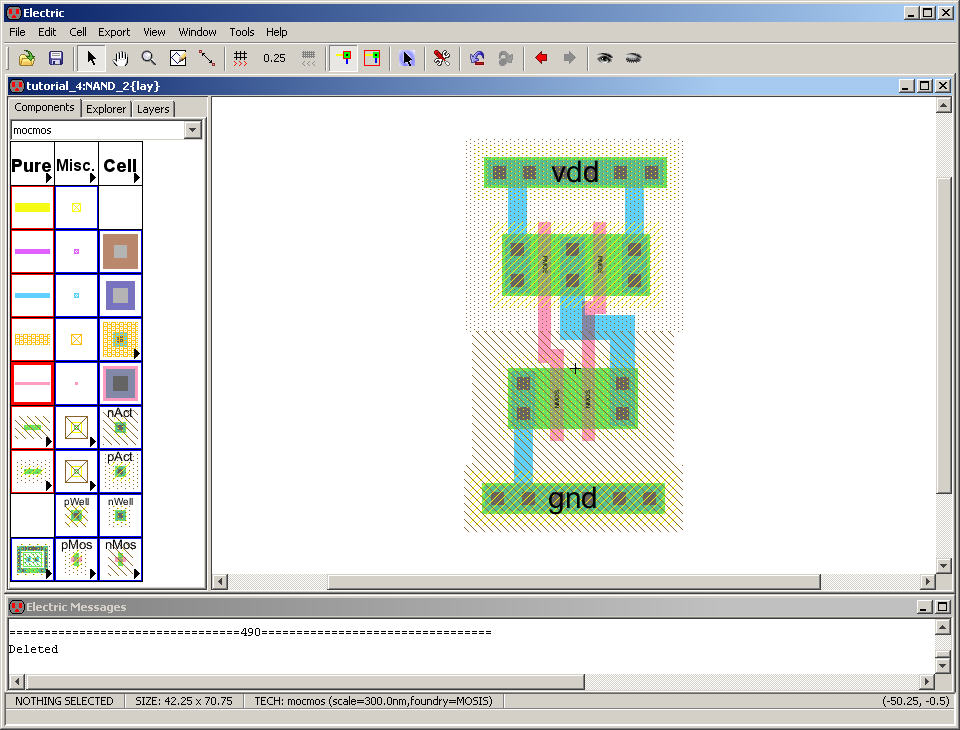
Connect
the gates of the Nodes together as seen below.
DRC
your layout to ensure that there aren’t errors.
Add
metal1-poly1 contact Nodes.
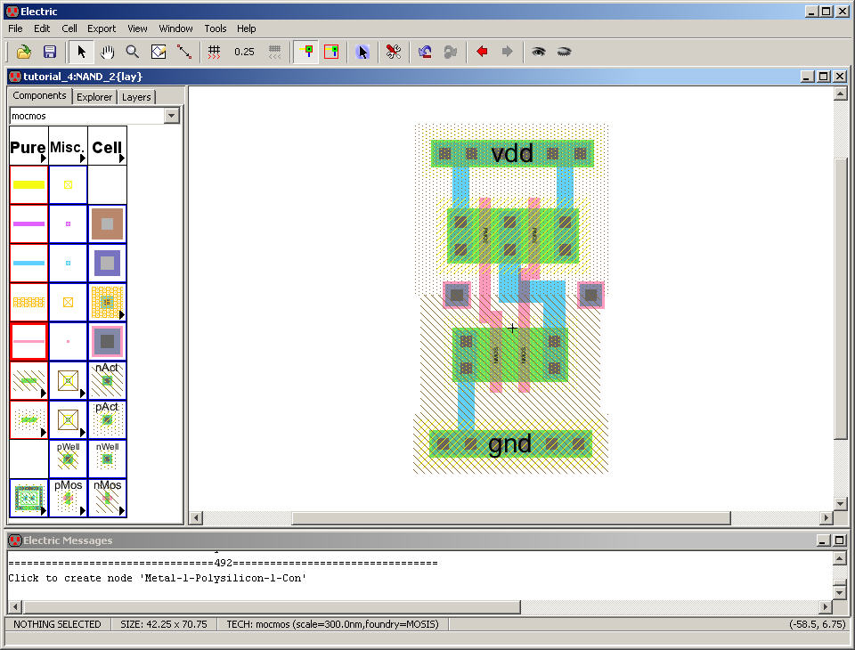
Add
poly1 Arcs to get the following.
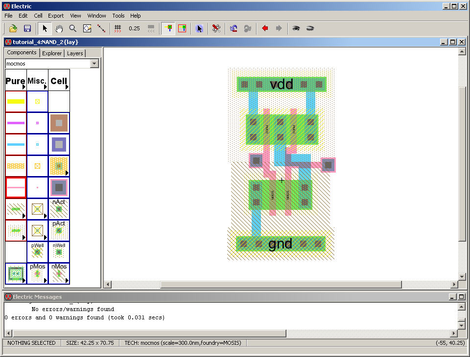
DRC
your layout.
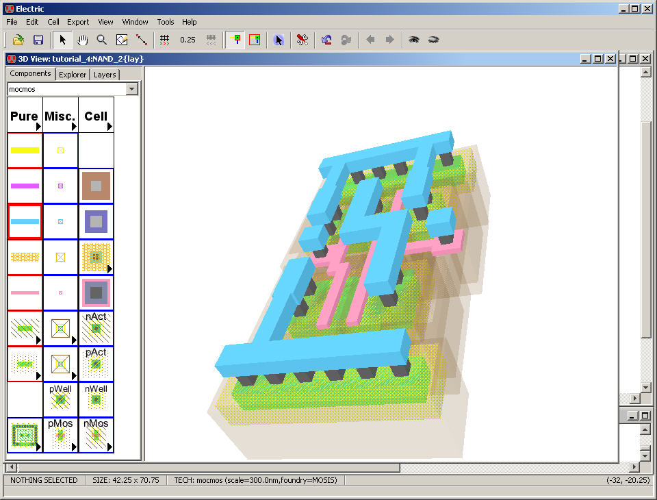
Below
is a 3D view of this layout created, ensuring Java3D is
installed on your computer, by going to Window -> 3D Window
-> 3D View
The
mouse is used to rotate the view. The mouse roller button
can be used to zoom in and out.
Add
metal1-metal2 contact Nodes as seen below.
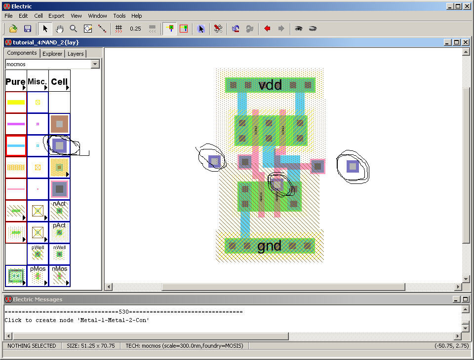
Using
a metal1 ARC connect the Nodes up as seen below.
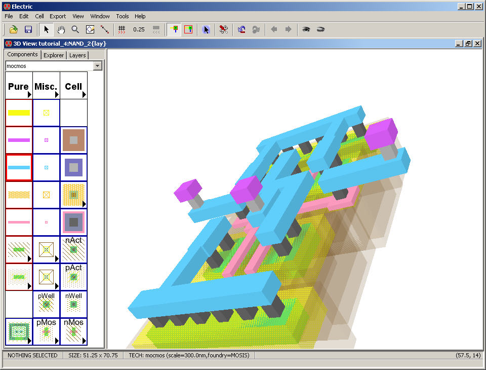
Here
is a 3D view of this layout.
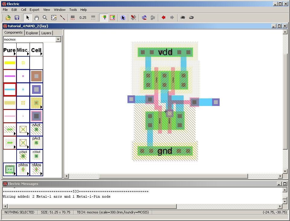
Let’s
move the metal1 to metal2 contacts and export them
(size up the Export’s text size to 4)
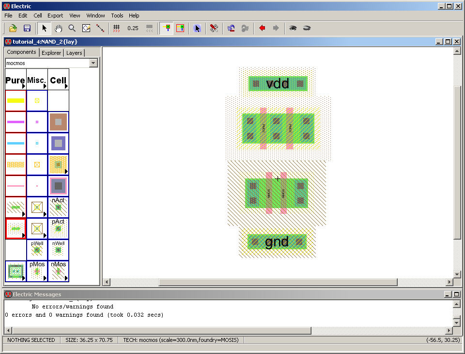
DRC
your layout to ensure there aren’t errors.
Well
Check your layout.
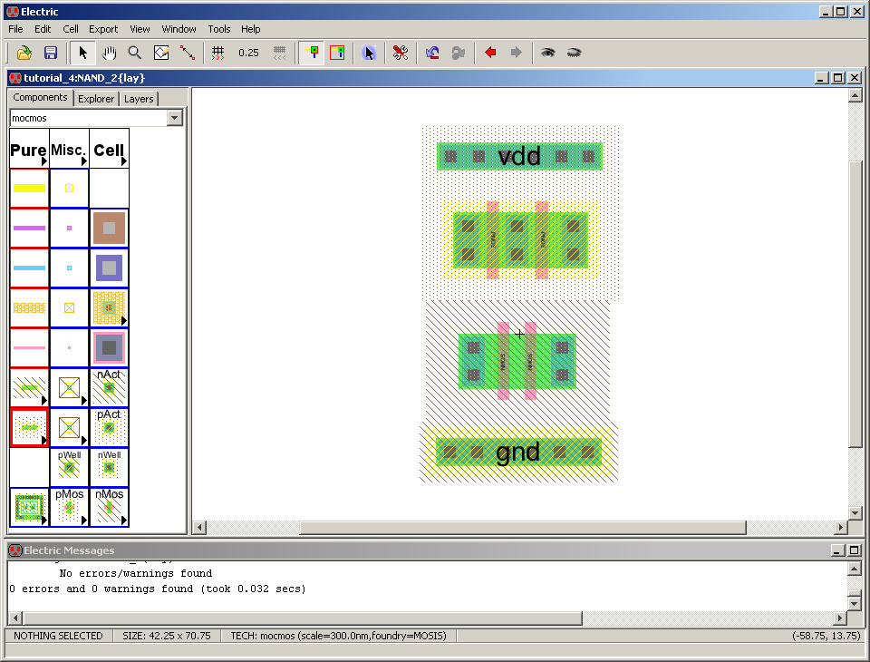
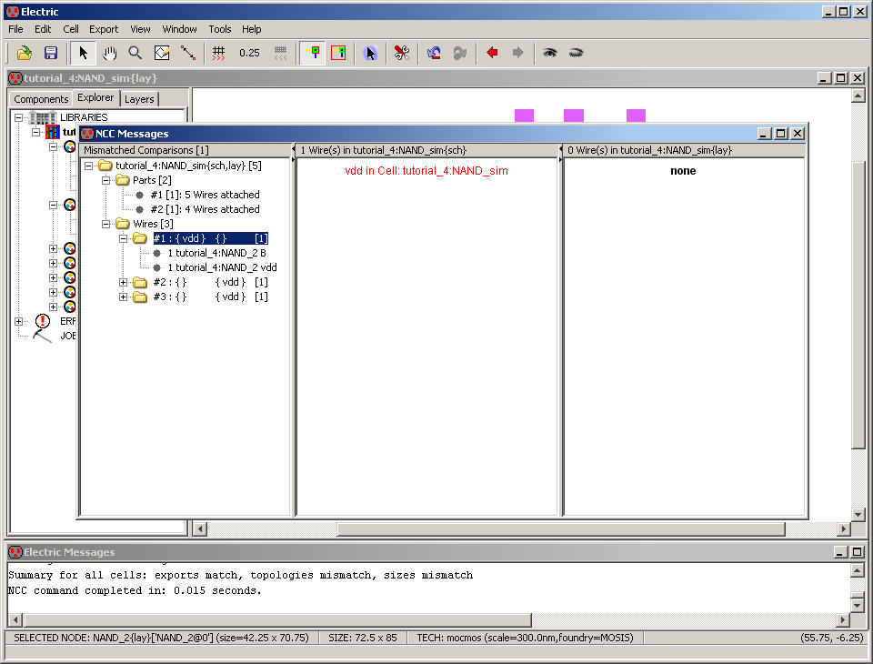
Finally
NCC the layout. We get errors.
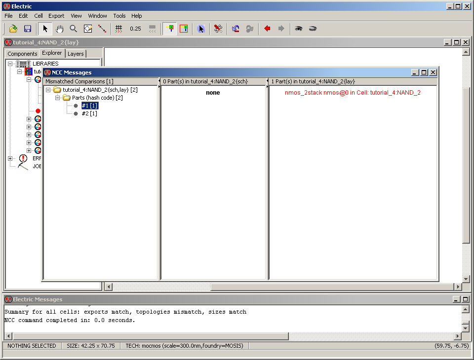
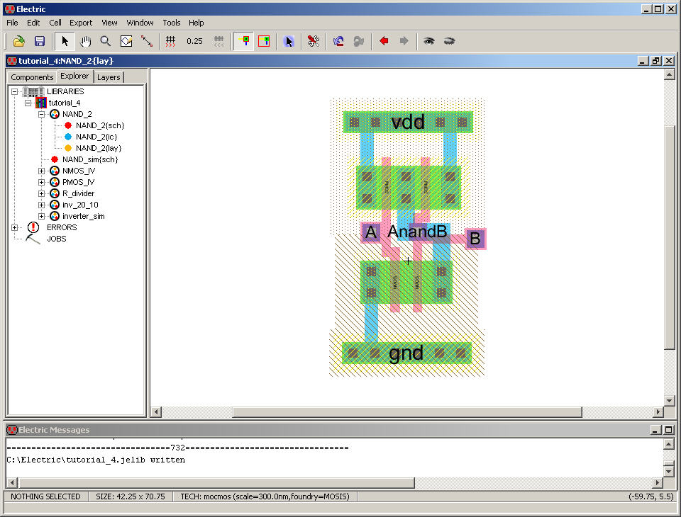
Inspecting
the layout we see the NMOS connected to ground has
its gate exported as A while in the schematic it’s exported as B.
All
we need to do is swap the exports in either the layout or
the schematic to make pass the NCC (aka LVS).
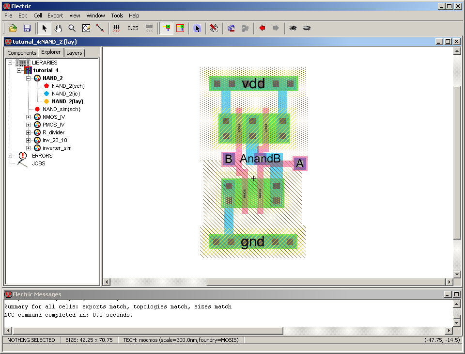
Swapping
the exports in the layout, below, we pass NCC.
Again, using Ctrl+click
is useful for cycling through
the selections.
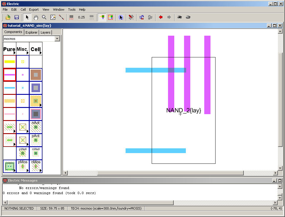
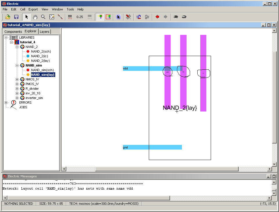
Okay,
let’s make the layout view of the NAND_sim
cell.
Instantiate
the NAND_2 layout into this cell and add Arcs
(see below).
DRC
the resulting layout to ensure no errors.
Label
the metal2 Arcs in, vdd,
and
out (to correspond to what we labeled them in the schematic).
Remember
that we have to export vdd
and gnd so that they
pass the well check test.
Also
remember we can only export Pins. Export vdd
and gnd now.
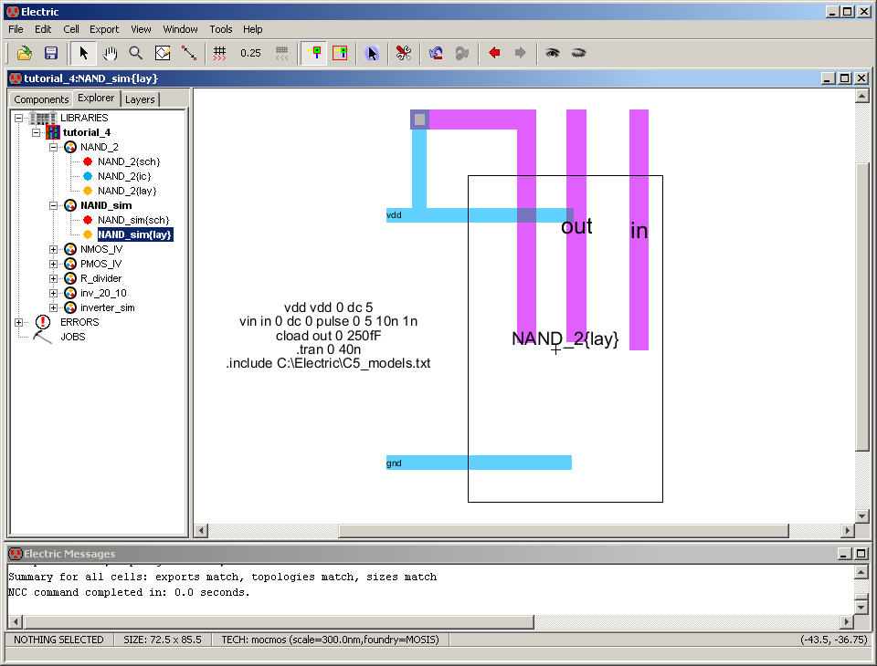
Copy
the Spice Code from the schematic view and increase the
text size to 3.
Note
that the size of the vdd
and gnd Exports is
acceptable; however, the Arc names are
difficult to see.
Increase
the Arc name text size to 5 then perform a DRC, Well
Check, and NCC.
The
layout/schematic don’t pass the NCC check.
When
we use the power symbol in the schematic we have to
export the a Pin on the corresponding Arc in the layout.
Let’s
simply connect the vdd
and
NAND input together in this layout as seen below.
DRC,
NCC, and Well Check the resulting layout (it should pass
now).
We
can now simulate the operation of this cell using LTspice
(do this now).
Save
the library.
This
is the end of the fourth tutorial.
For
your reference the final jelib
used in this tutorial
is located in tutorial_4.jelib