Electric VLSI Design System
Tutorials
from CMOSedu.com
(Return)
Tutorial
1 – Layout and simulation of a resistive voltage divider
This
tutorial will introduce you to the Electric VLSI design
system.
It’s
assumed that Electric (version 8.10 or later) and
LTspice have been installed properly on your computer following the
instructions
here
and here.
With
this assumption all layout and simulation work will be
done (saved) in C:/Electric (where the Electric jar file resides).
Ensure
that you have increased the memory in your JVM as
instructed above.
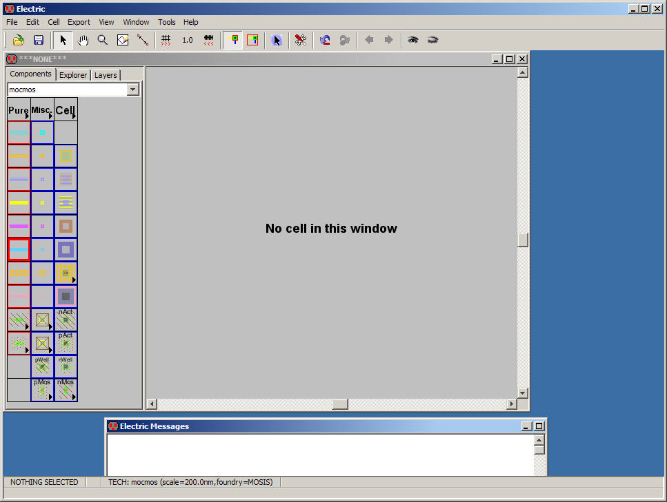
Start
Electric. You should see the following window.
Note
that this shouldn’t be the first time you’ve started
Electric since you’ve followed the instructions above and have set
LTspice up
for use with Electric and have increased the JVM.
This
is mentioned since it’s possible to simply save the
Electric jar file to the desktop, double-click on it, to start/use
Electric as discussed
here.
Next
go to menu item Window -> Color Schemes -> White
Background Colors
Using
a white background will be useful in these tutorials so
that ink is minimized if they are printed out
It’s
often preferable to use a black background colors to ease
the stress on your eyes ;-)
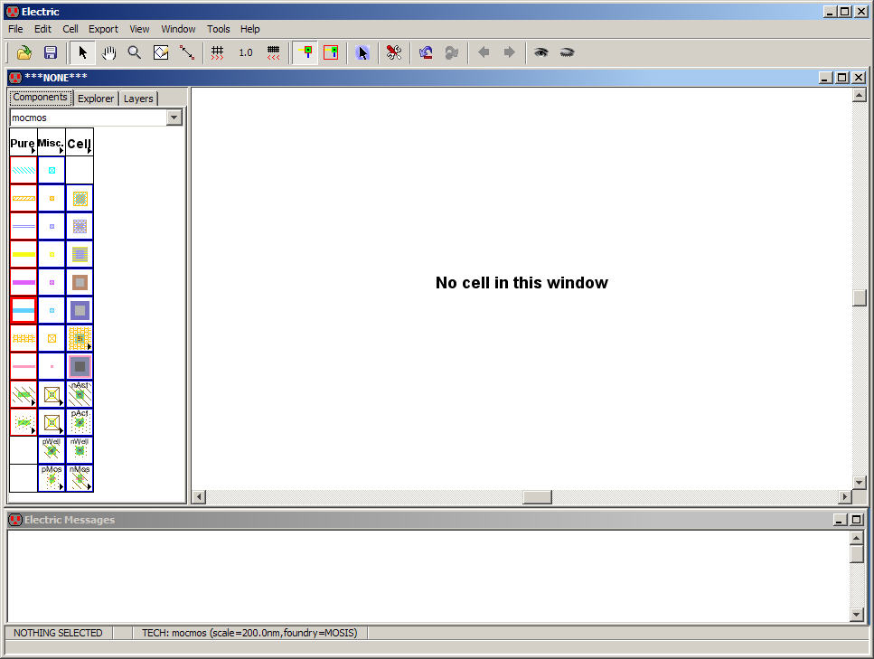
Adjust
the sizes of the windows to fill the available space
as seen below.
We’ll
set Electric up for use in ON Semiconductor’s C5
process and
fabrication through MOSIS.
This
process has two layers of polysilicon
to make a poly1-poly2 capacitor, 3 layers of metal, and a
hi-res
layer to block the implant, and thus decrease in
resistance, of poly2 to fabricate higher-value
(than
what we would get with poly1) poly2 resistors.
This
tutorial uses the MOSIS scalable CMOS (SCMOS) submicron design rules.
While
the C5 process is an n-well process we’ll still draw
the p-well, which will be ignored during fabrication, just to make the
layouts
more portable between processes.
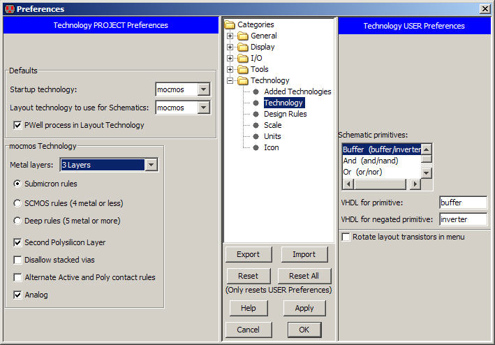
Next,
go to File -> Preferences (or just hit the
wrench/screwdriver menu icon) then Technology -> Technology to
get to the
window seen below.
Change
the information to match what is seen below.
Note
that the “Analog” Technology is selected.
This
selection shows the resistor and capacitor Nodes in the
Component menu (discussed shortly).
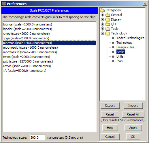
Next,
the scale (lambda) for the C5 process is 300
nm using the MOSIS Scalable CMOS (mocmos
technology in Electric, see image above) submicron design rules.
To
set the scale go to File -> Preferences ->
Technology -> Scale and set mocmos
scale to 300 nm
as seen below.
Press
OK to exit.
Select
Mark All Libs in the
next
Window to indicate you want all of the libraries marked with these
changes.
Here
are my preferences (right click and save as), electricPrefs.xml which
can be loaded if there are
problems or to ensure consistency through the remainder of the
tutorial.
File
-> Import -> User Preferences followed by
navigating to where my preferences were saved imports these preferences
if
there are problems.
We
now have Electric set up to fabricate a chip in the C5
process via MOSIS (technology code is SCN3ME_SUBM with a lambda of 0.3
um, see
the MOSIS page here at CMOSedu.com).
Go
to File -> Save Library As -> tutorial_1.jelib
Next
let’s begin to draw the schematic of a resistive
divider.
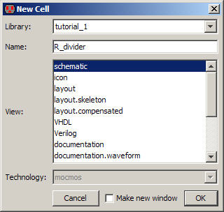
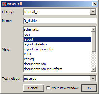
Go
to Cell -> New Cell and enter the cell name (R_divider)
and
view (schematic) seen below.
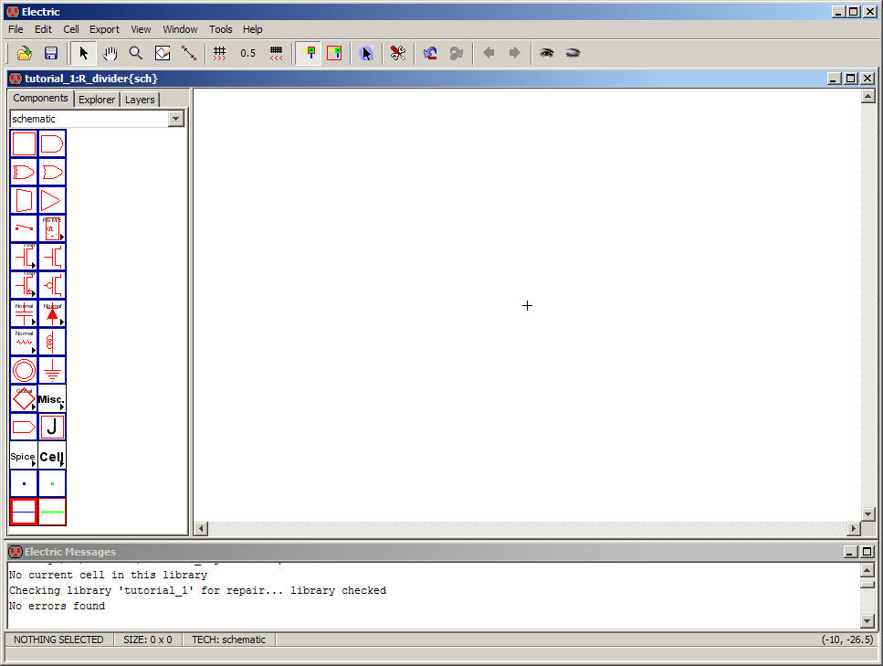
After
selecting the Component tab on the left side of the
window we get the following.
The
library name and cell name are seen above the Components,
Explorer (for looking at the cells in your library), and Layers (useful
in
layouts to turn on/off the display of certain layers).
In
the Component menu there is a box containing a resistor
and the word “Normal.”
Click
on the arrowhead in this box and select N-Well. This
selects the N-Well schematic resistor Node.
In
Electric-speak a Node is a component used in a schematic
or layout. Examples of Nodes include transistors, resistors,
capacitors, etc.
An Arc, which
we’ll discuss shortly, is used to connect Nodes together to form
schematics or
layouts. A wire is an example Arc in a schematic.
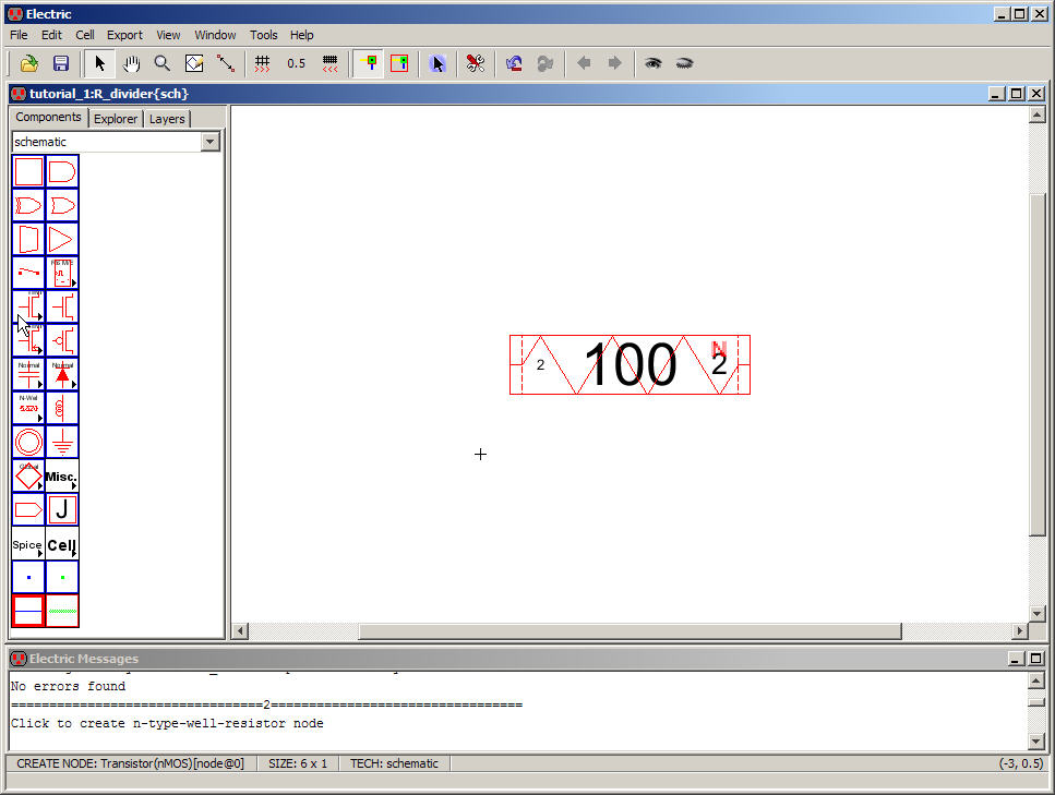
Place
the N-Well schematic resistor Node into the drawing
area as seen below (left click the mouse button to place the Node).
Use
the Window menu commands to zoom in/out, fit, etc. the
view after placing the Node.
All
Nodes have a highlight box that turns on, to indicate
that the Node may be selected, when the cursor is placed over it.
When
a layout/schematic contains Nodes whose highlight boxes
overlap the selection of a particular Node can be cycled through by
pressing
the Ctrl+mouse click
(very useful in complex layout).
Pressing
Shift while clicking the left mouse button
selects/de-selects an item (again, very useful).
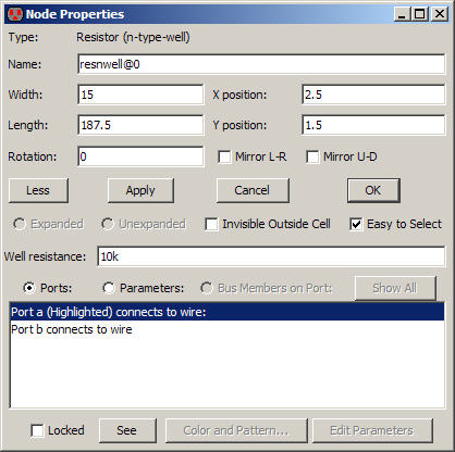
Select,
by clicking on Node, the N-Well resistive Node.
Next
go to Edit -> Properties -> Object Properties (or
simply Ctrl+I) to edit
the properties of this Node,
see below.
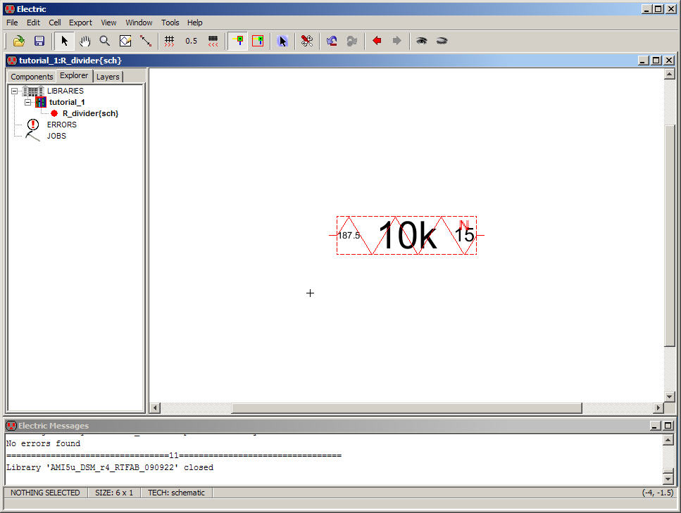
The
sheet resistance of n-well in the C5 process is roughly 800 ohms.
The
minimum width of n-well is 12 lambda so let’s make a 10k
resistor using a width of 15 and a length 187.5 (since sheet resistance
varies
we could round to 185).
Enter
the values as seen below.
If
the field for the Well resistance isn’t showing hit the
More button.
We’ll
use these same values when doing the corresponding
layout.
After
pressing OK (not the X in the top right side of the
window which would ignore your changes) we get the following.
This
is a schematic representation of a 10k N-Well resistor.
Before
moving on go to Tools -> DRC -> Check
Hierarchically (or just hit F5) to check the schematic for errors.
The
Electric Message window will indicate that there aren’t
any errors.
It’s
a good idea to get used to looking at the messages in
this window.
Listening
to Electric can really save time ;-)
Let’s
next make a layout corresponding to this schematic-view
cell.
Again,
go to the menu item Cell -> New Cell and enter the
Name and View seen below.
This
will create a group of cells.
Clicking
on the “+” sign adjacent to the cell group (R_divider) name
gives the following.
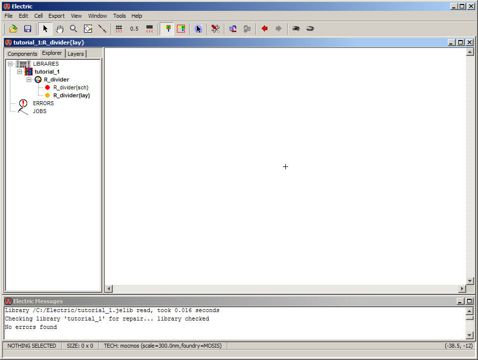
The
red circle indicates a schematic view while the yellow
circle indicates the cell’s layout view.
Blue
indicates an icon while black may indicate a Verilog
view (among others).
Notice,
above the tabs, that the library name is tutorial_1
while the active cell name is R_divider{lay}.
Also
notice at the bottom of the screen is an indication of
the technology and scale.
When
we start doing layout this area will also the indicate x
and y position of the cursor.
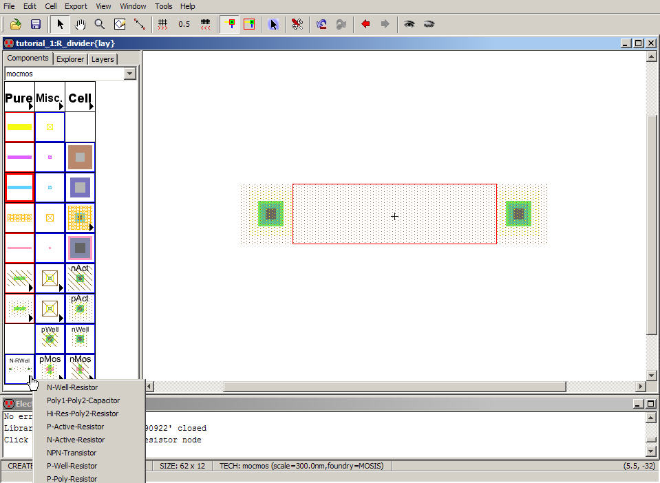
Next,
go to the Components tab and select the N-well resistor
Node in the bottom left-hand side of the menu (click on the arrowhead).
Note
that if this menu item isn’t available, as seen below,
then you didn’t select the Analog option in the preferences near the
beginning
of this tutorial.
Set
the size (Edit -> Properties -> Object Properties
or better yet simply hit Ctrl+I) of the N-Well
resistor to, as above, L=15, W=187.5,
and a resistance of 10k.
After
fitting the display using the Window menu item we get the
following.
Notice,
like the schematic N-Well resistor Node, that this
Node is selected by moving the mouse over the Node’s highlight box and
left
clicking on the Node.
Also
note, again like the corresponding schematic Node, that
this Node has two ports for connection to Arcs.
In
the figure below we moved the cursor towards the left port
of the Node so that clicking on the Node selects this port.
To
verify the layout doesn’t contain design rule errors go to
Tools -> DRC -> Check Hierarchically (or just hit F5) to
perform a design
rule check.
From
this point on “pressing F5” will be equivalent to saying
that we are doing a design rule check of a layout or checking a
schematic.
After
pressing F5 we see in the Electric Message window that
there aren’t any errors (so let’s make one).
Edit
the properties of the N-Well resistor Node above so that
the width is 5.
Press
F5 to run the DRC. We get the following.
Notice
how the Electric Message window tells us that to step
through the errors we press the greater-than key, >, to go
forward through
the errors or the less-than key, < to go backwards through the
errors
Pressing
OK above and then > gives the following view
(after zooming in around the flashing red and black box indicating the
error’s
location).
Notice
the type of error is indicated in the Message window.
Pressing
Ctrl+Z a few times gets
back
to the case where W =15 (or selecting the resistor Node and hitting Ctrl+I allows us to change it
back manually)
Press
F5 to verify the layout is DRC free.
Then
use the menu item Window -> Fill Window to zoom back
out.
At
this point let’s verify that the schematic and layout
views of the R_divider
cells are equivalent.
This
layout versus schematic (LVS) verification is performed
in Electric using Network Consistency Checking (NCC).
To
perform an NCC go to Tools -> NCC -> Schematic and
Layout Views of Cell in Current Window.
There
shouldn’t be any errors. However, if there are a table
pops up that allows you to click on the error to view it in a new
window.
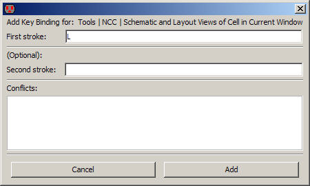
Since
we’ll be doing an NCC quite often let’s setup a key
that we can press on the keyboard to perform this menu selection.
In
other words let’s bind a key to this menu selection.
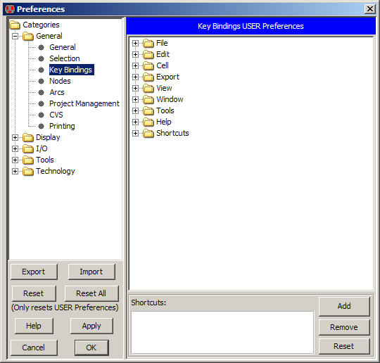
In
the menu go to File -> Preferences -> General ->
Key Bindings as seen below
On
the right, navigate to Tools -> NCC -> Schematic and
Layout Views of Cell in Current Window
Once
this menu item is selected Add and bind L to this menu
item (so we can do an NCC, aka LVS, each time we press L)
Note
that although we pressed lowercase l it shows up as
uppercase L below. So lower case l will be bound to the NCC command.
Press
Add again in the window seen below.
This
next part is important.
If
a conflict exists when binding a key then Electric will
tell you after you have added the key and pressed Add.
You
need to “Remove All” conflicts (important).
If
you don’t select Remove All Conflicts then a key may be
bound to two or more menu items causing crazy behavior!
Before
connecting resistors together to form a voltage divider
let’s talk about the connection of the n-well and p-substrate.
Since
the C5 process used in this tutorial is an n-well
process the p-type substrate is common to all NMOS devices and grounded.
One
of the electrical rule checks (ERCs) is to verify that
the p-well (in our case this means p-substrate) is always connected to
ground.
Further,
in this n-well process, if the design contains only
digital circuits then we always want the n-well to be connected to VDD.
To
setup the ERC Well Check go to Preferences -> Tools
-> Well Check as seen below
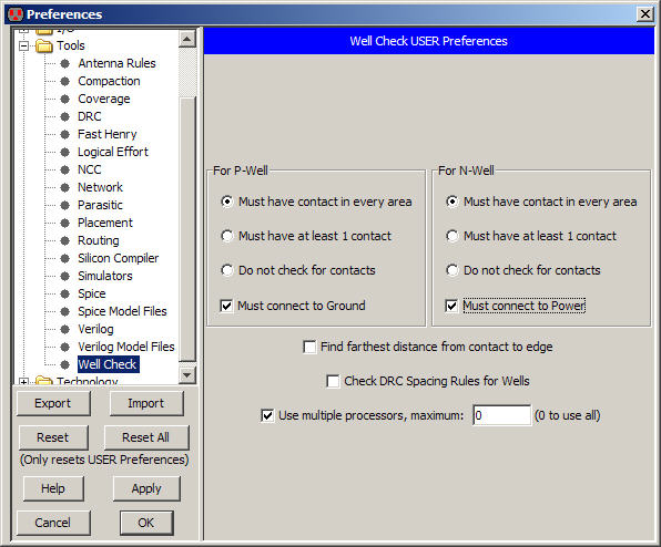
In
all cases we want to verify that a contact is found in
every area (floating wells are bad!).
We
also want to verify that the p-substrate (p-well) is
always tied to ground.
However,
as just mentioned, we only want to verify that the
n-well is tied to vdd
(power, yes, we’ll use
lowercase) if the chip is a digital only design (no N-Well resistors)
Running
the Well Checker (Tools -> ERC -> Check Wells)
on the resistor layout above reports the following errors.
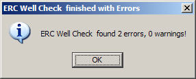
To
eliminate these errors, since our design isn’t only
digital (hence why we check the analog box when we setup our
preferences at the
beginning of the tutorial) change the settings to the following.
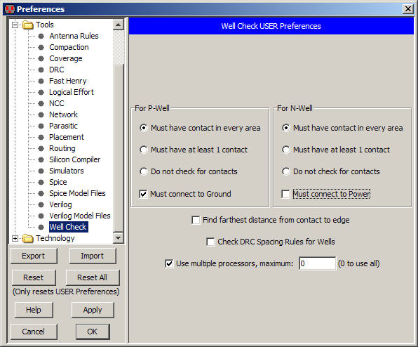
Mark
All Libs to indicate
you want
all currently open libraries to use these preferences.
Running
the Well Checker again on the resistor’s layout above
doesn’t report errors (which is good).
Next
let’s wire up a resistive divider.
Go
back, using the Explorer, to the schematic view of the R_divider cell.
Select
the N-Well resistor Node and then hit Ctrl+C
to copy the Node.
Next
click somewhere in the drawing area to deselect the
Node. Press Ctrl+V and
then left-click the mouse to
paste the copied Node.
Don’t
worry about making a mistake. Ctrl-Z works really well
to back you up for another try.
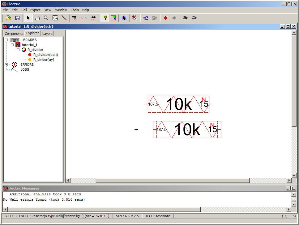
An
example result is seen below (where I zoomed out a bit
prior to capturing the screen image).
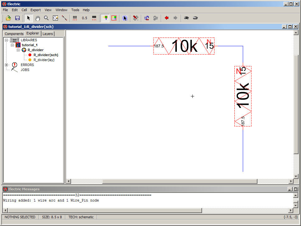
Next
select the bottom resistor Node and use the menu item
Edit -> Rotate -> 90 Degrees Counterclockwise (or just
simply Ctrl+J) to get
the following.
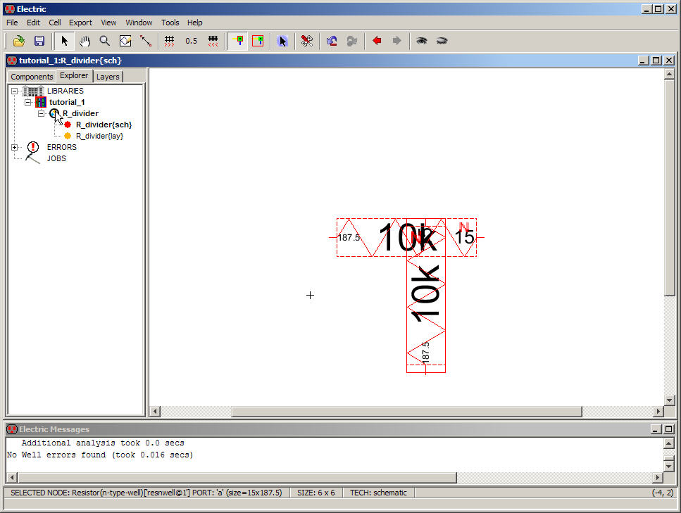
Move
the resistors apart so the horizontal Node is above the
vertical Node.
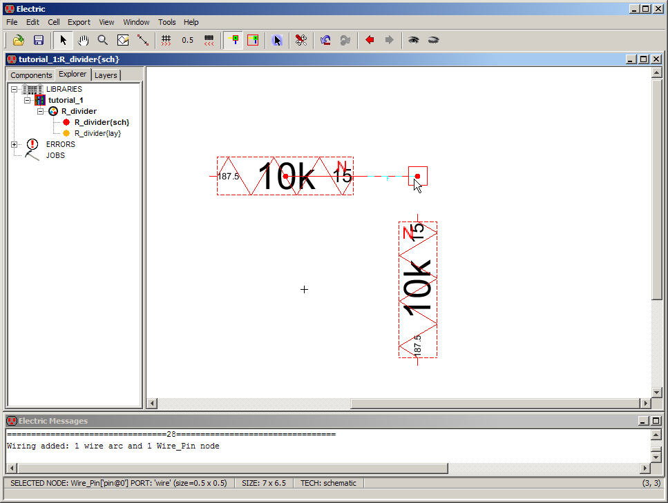
Next
select the top Nodes right port by clicking near it with
the left mouse button.
This
makes this port active and thus ready of a wire
connection.
Move
the mouse cursor so it’s above the vertical Node and
RIGHT click the mouse (using the RIGHT mouse button may take a little
getting
used to)
The
result is seen below.
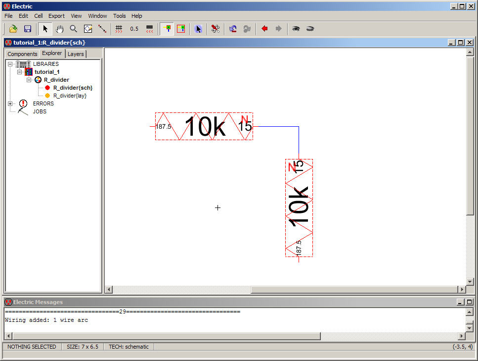
Next
move the mouse cursor over the top port of the left
(vertical) resistor Node and RIGHT click the mouse button.
The
following is the result (zoom out or in as required).
Now
is a good time to check the schematic for errors by
pressing F5.
Note
that if you put your cursor over the corner in the wire
you will see a Pin
Pins
can be moved as well as the wires in schematics
A
common error in a schematic is having unnecessary Pins.
Unnecessary
Pins can be removed by going to the menu item
Edit -> Cleanup Cell -> Cleanup Pins
I
set up my key bindings so that F4 cleans up unnecessary
Pins everywhere (available in electricPrefs.xml,
right click to save as then File -> Import -> User
Preferences)
Next
let’s add a couple more wires as seen below.
Remember
to left click for selecting a port on a Node and
right click to add the Arc (wire).
We
could add symbols for ground and a voltage source from the
component menu but instead let’s simply label the Arcs (the wires) in
the
schematic.
Note
that the SPICE components are accessed by clicking on
the arrowhead in box under the Component menu labeled SPICE
Select
an Arc and press Ctrl+I
to
edit the properties of the Arc or simply just double-click on the Arc.
Label
the Arcs as seen below. Note that the bottom Arc is
label gnd (a universal
name for ground in SPICE, yes,
use lowercase as we did for vdd)
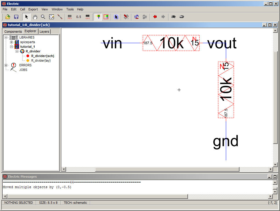
Move
the Arc names until they are aesthetically pleasing (see
example below).
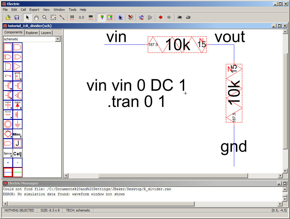
Next,
click on the arrowhead in the Misc box in the Component
menu to add SPICE code to the schematic as seen below.
Place
the SPICE code in the schematic and use Ctrl+I
to edit its properties.
Ensure,
in the SPICE code property box, that the Multi-line
Text box is checked.
Add
the text seen below for specifying a SPICE transient
analysis and an input voltage source.
Press
F5 to check the schematic.
Also
save the library.
Again,
as mentioned at the beginning of this tutorial,
LTspice must be setup with Electric.
To
simulate this schematic go to Tools -> Simulation
(Spice) -> Write Spice Deck
The
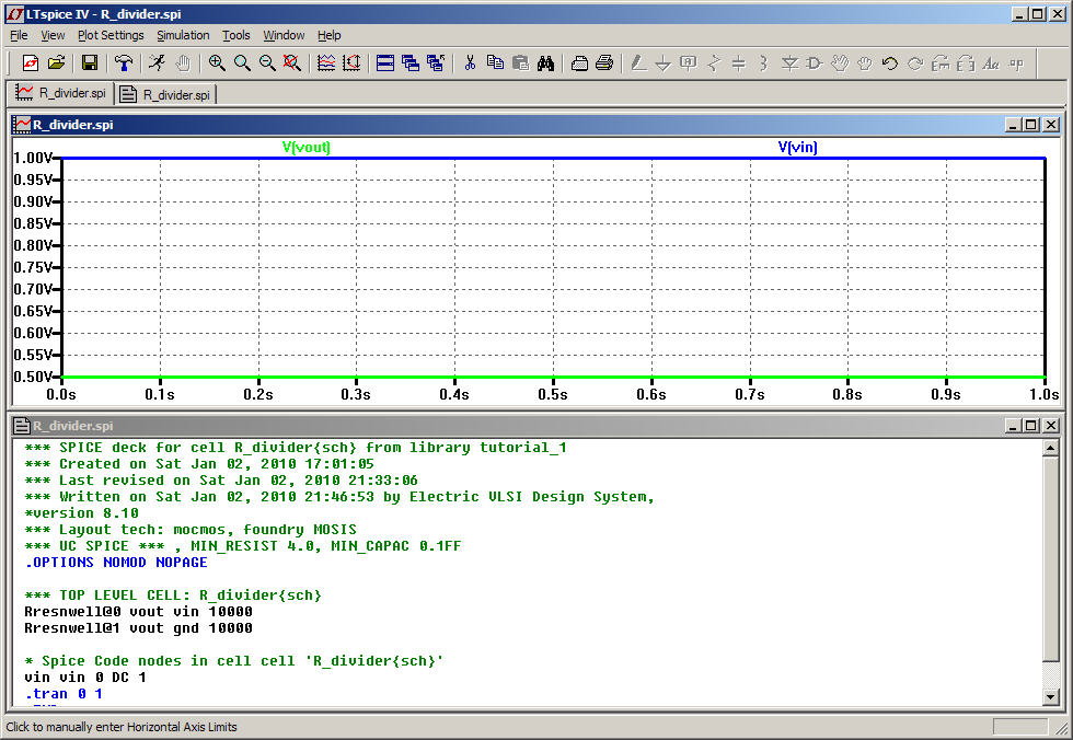
following LTspice window will open.
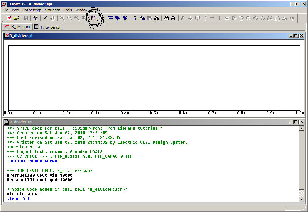
Click
on the circled icon above to show the waveforms
available for plotting.
Select
V(vout) and V(vin) to display the following.
The
LTpsice waveform plotter
is
very useful but doesn’t allow for cross-probing between SPICE results
and
Electric layout/schematics.
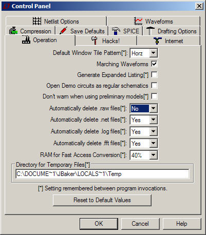
To
plot SPICE results using Electric’s probe first ensure,
via (in LTspice, not Electric) Tools -> Control Panel ->
Operation (see
below) that waveform files (.raw files) are not automatically deleted.
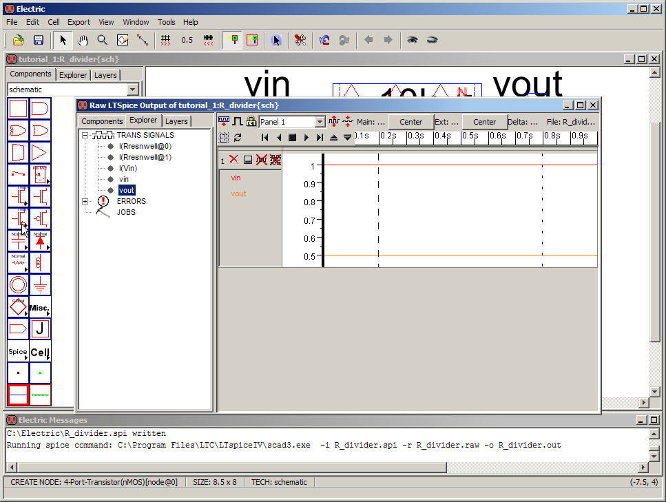
When
LTspice is closed, with the setups seen here,
Electric’s probe will run as seen below (after the explorer was used to
select vin and vout).
Note
that these Windows can be tiled and the same commands used
for zooming and expanding in the layout/schematic views can also be
used here.
To
bypass the LTspice Window and use Electric’s probe only
change from the –i
(interactive) to –b (batch) modes
as mentioned when setting LTspice up for use with Electric
Next
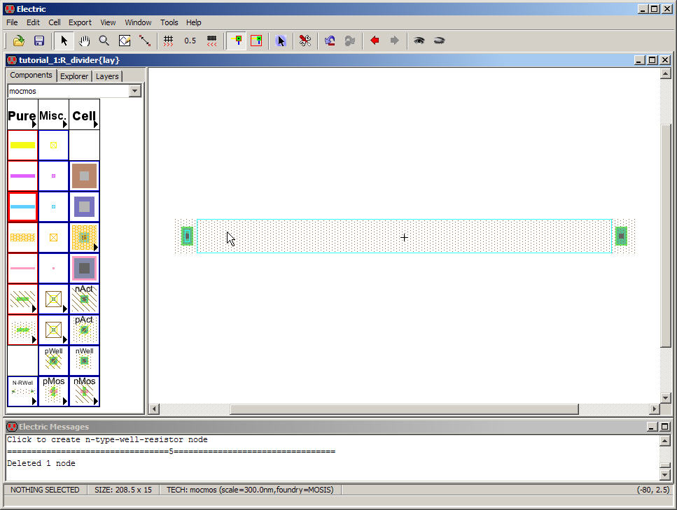
let’s layout the resistive divider.
Open
the layout view of the R_divider
cell then copy/paste (Ctrl+C/Ctrl+V)
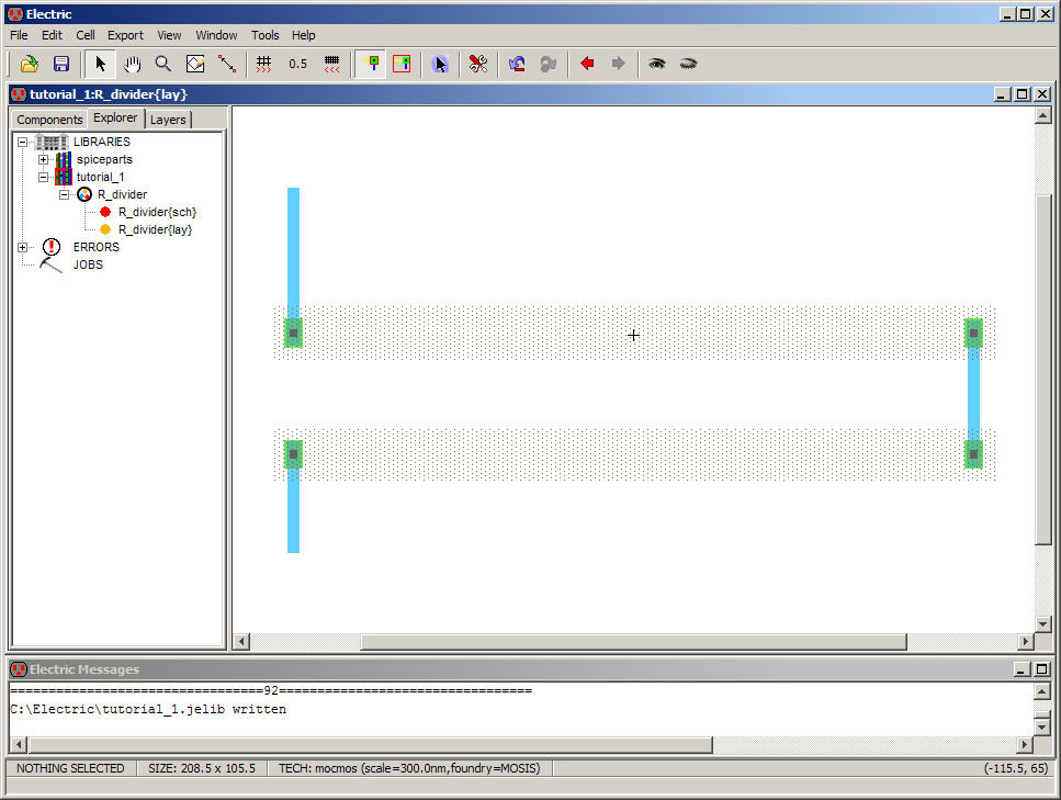
an additional resistor as seen below.
To
move the resistor Node (the layout of an N-Well resistor)
either the mouse can be used or you can select the Node and use the
keyboard
arrows.
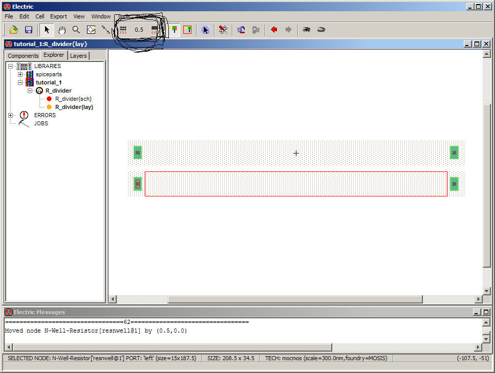
The
menu items circled in this figure above increase, set,
and decrease the grid alignment. It’s set at 0.5 scale above.
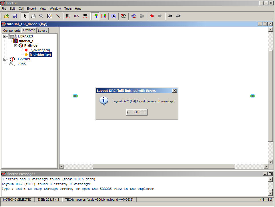
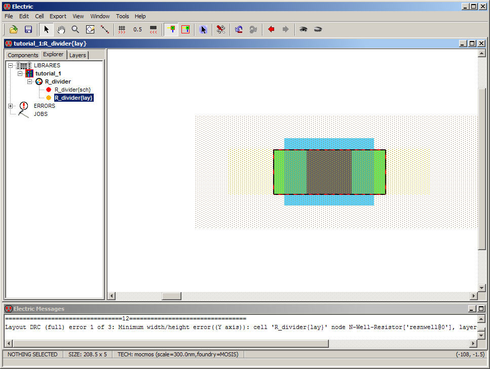
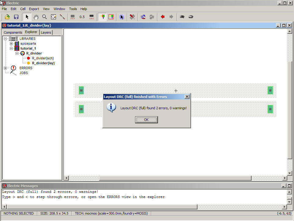
Running
a DRC (pressing F5) on the above layout results in
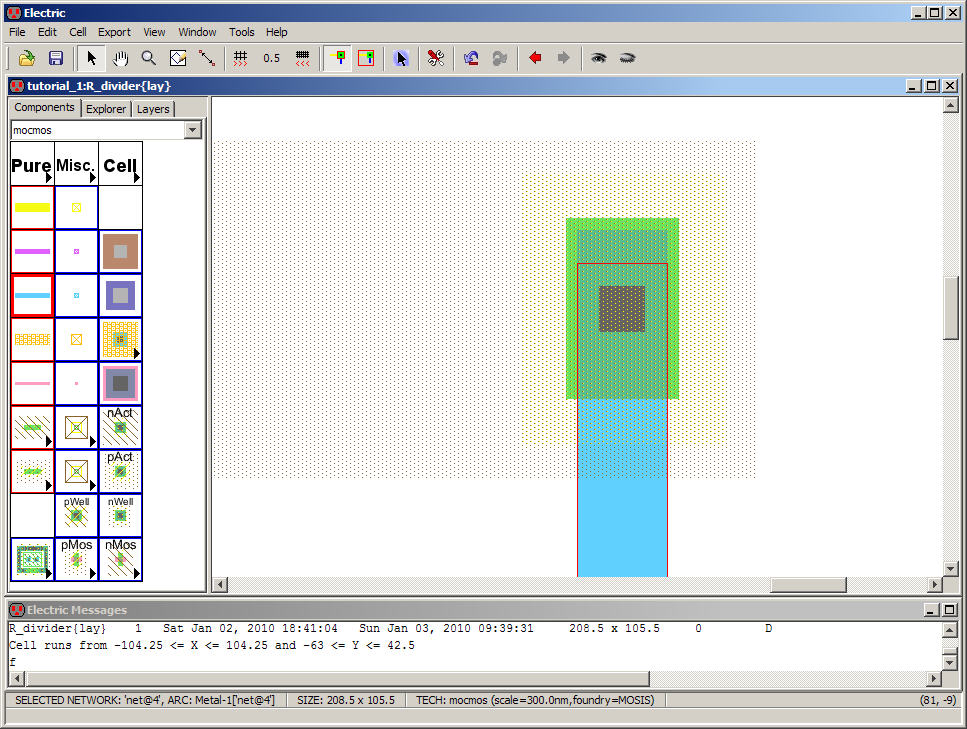
the following figure.
By
pressing > we see that there is too little space
between the N-wells.
Move
the Nodes apart until the layout passes the DRCs.
Next
move the mouse over the right side of the top Node’s highlight
box and left click (to select the top node and its right port).
RIGHT
clicking (over the right side of the highlight
box on the bottom resistor
node) will connect the metal1 Arc to the bottom resistor.
Note
that when you RIGHT click to connect the node, you have
to be over the right side of the highlight box else you won’t connect
the two
ports
and
the resistor will fail DRCs (you will generate an Arc
that isn’t connected).
DRC
your layout to verify there aren’t errors.
Before
labeling the Arcs in this layout and simulating (we’re
almost done!) let’s provide some comments.
First,
how many Pins are found in this layout? Answer, 2.
The
ends of the metal Arcs that aren’t connected to anything
contain Pins.
There
would also be Pins at any bends or corners in the metal
Arcs.
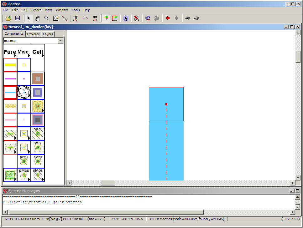
Below
is a zoomed in view of the top Pin (this Pin has been
selected).
Also,
in the Component menu below the metal1 Pin is circled.
Placing
a Pin in a layout is useful for drawing an Arc
without first having a Node.
Of
course, with this Pin selected, you can RIGHT click
somewhere in the layout and a metal1 Arc is drawn to that point.
Please
experiment with drawing Arcs from Pins, these Nodes,
and to other Arcs.
Remember
you can always it Ctrl+Z
to undo your work so don’t worry about “mistakes”
Next
zoom in on the area seen below.
Let’s
increase the width of the metal1 Arc so that it matches
the connection to the N-Well resistor.
Select
the Arc and hit Ctrl+I
(or
Edit -> Properties -> Object Properties noting that in my
key bindings
use Q in place of Ctrl+I)
The
following window should appear.
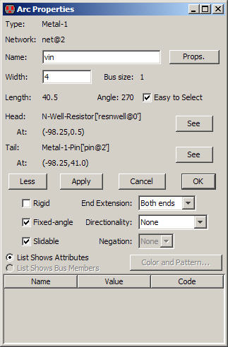
Change
the width of the Arc to 4 and hit OK (not the X at the
top right of the window which cancels your change).
Note
the field “End Extension”
This
field specifies how the ends of the Arc are drawn. We’ll
talk about the End Extensions in greater detail in the coming tutorials.
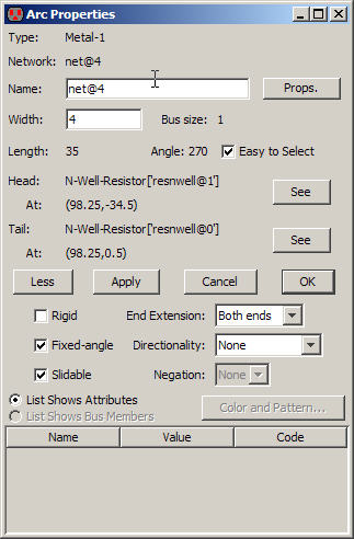
After
changing the Arc’s width to 4 the layout changes to the
following.
Change
all of the Arcs in the layout so that they are 4 wide
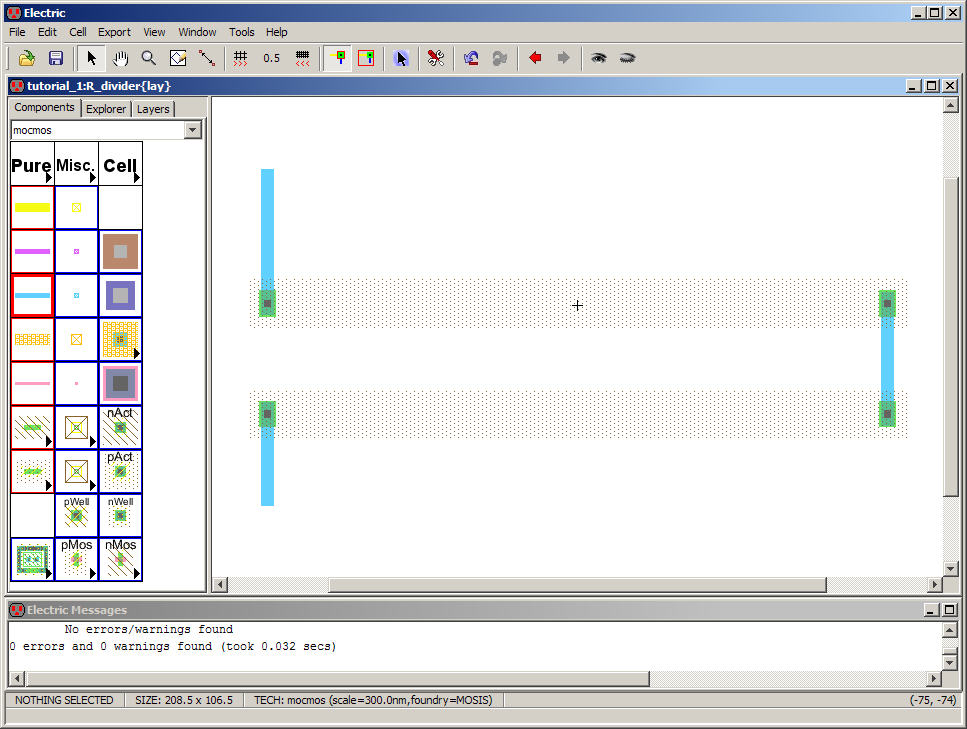
and then fit the layout to the window, as seen below.
Remember
to DRC the cell when you are done.
Next,
just like we did in the schematic, let’s label the
Arcs: vin, vout, and gnd.
To
label the Arc we select it and press Ctrl+I
(or just double click on the Arc).
Change
the name of each Arc (knowing the Arc connecting the
two resistors has to have the name vout)
as indicated
below.
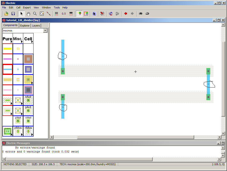
The
result is seen below.
The
names are circled but we can’t see them!
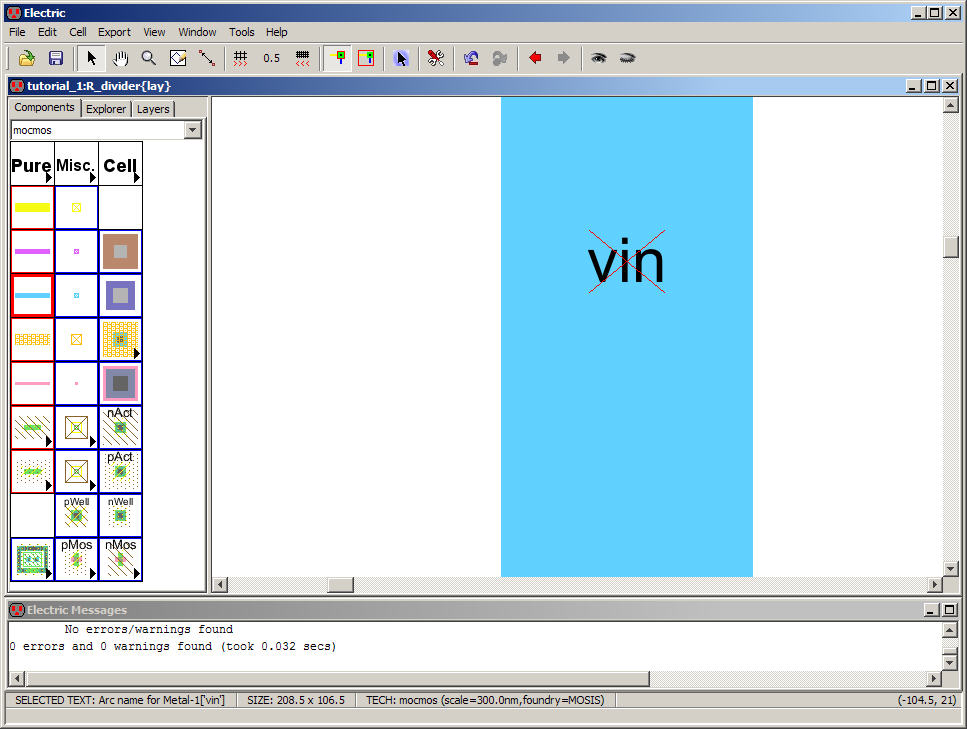
Zoom
in around the Arc name and select it as seen below.
Using
Ctrl+click may be very
useful
here.
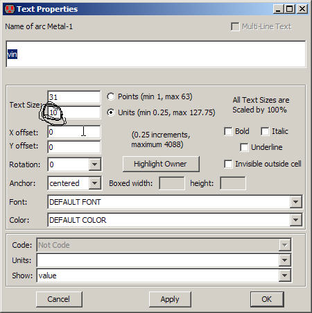
Edit
the properties of this text, the Arc’s name, by pressing
Ctrl+I.
Change
the text size from 1 to 10 as seen below.
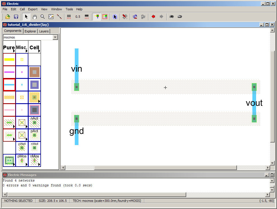
Change
the size of all of the other Arc names resulting in
the following.
At
this point this cell should be DRC clean (meaning when you
press F5 you don’t get any errors). Verify this now.
This
layout cell should also match the schematic cell. Verify
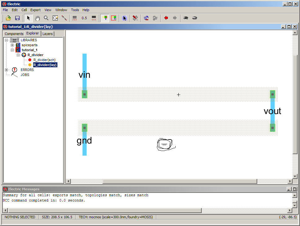
this by running the NCC (aka LVS check).
Note
that the names of the Arcs don’t have to match for the
cells to pass NCC. The Arc names are useful for humans but don’t affect
circuit
operation ;-)
We
are ready to simulate the layout view off this cell.
Let’s
open up the schematic view of the cell and copy the
SPICE code (select, Ctrl+C).
Go
back to the layout view and paste the SPICE code as seen
below (the SPICE code is circled).
Change
the size of the text used in the SPICE code to 10 (you
should know how to do this now).
Also,
let’s change the Text size of the resistor’s value to
10 so we can see the resistor’s value.
The
results are seen below.
Run
a DRC, NCC, and a Well Check to ensure that there aren’t
any errors (there shouldn’t be)
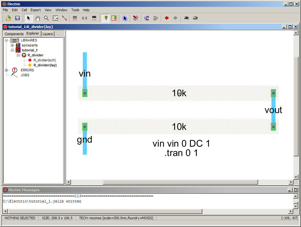
This
cell can be simulated following the same steps used for
simulating the schematic view above.
Simulate
this cell using LTspice now.
This
is the end of the first tutorial.
For
your reference the final jelib
(Electric library) used in this tutorial is located in tutorial_1.jelib