Electric
VLSI Design
System
Tutorials
from CMOSedu.com (Return)
Tutorial
2 – Layout and simulating the IV curves of PMOS and NMOS devices
In
this tutorial we’ll layout and simulate the operation of
NMOS and PMOS transistors using the setups, and C5 process, from Tutorial 1.
To
begin, use Electric to open the jelib
we used in tutorial 1, tutorial_1.jelib
(right click to save to C:\Electric).
Save
this library as tutorial_2.jelib,
again in C:\Electric.
Next
save the file C5_models.txt
to C:\Electric for SPICE simulations.
This
file contains the MOSFET models for the C5 process.
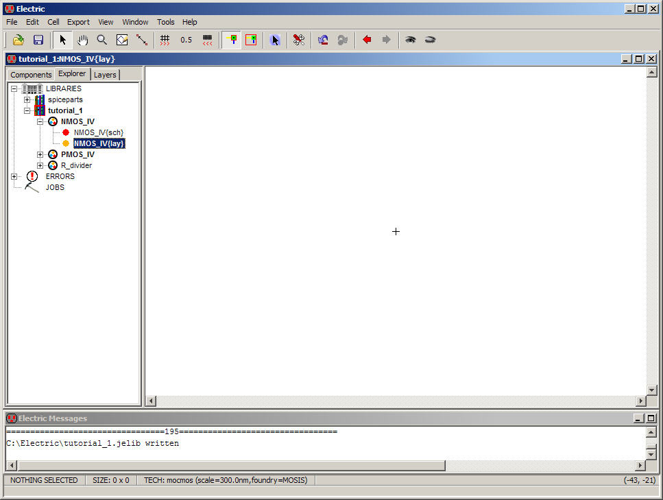
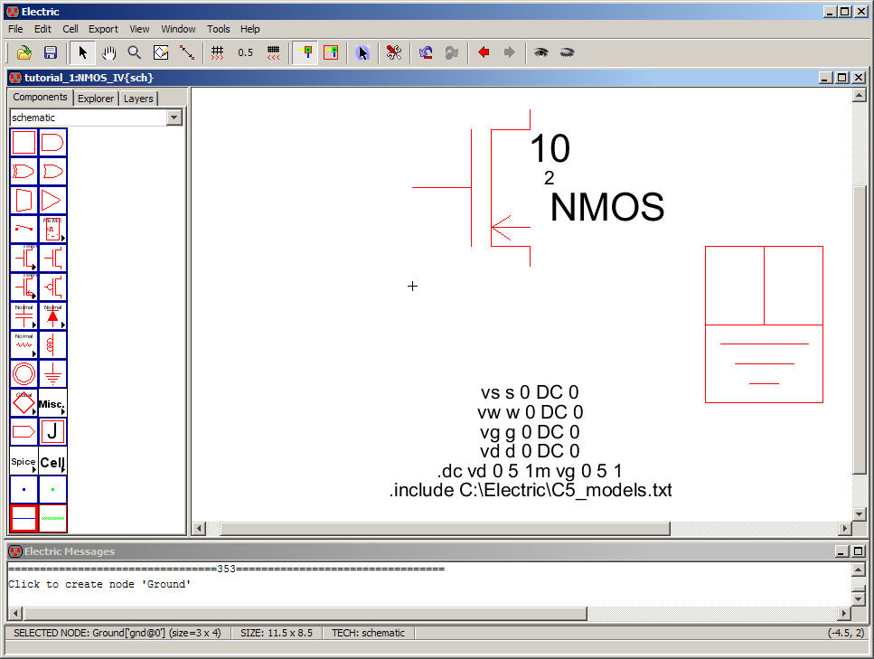
When
finished create new cell, a schematic called NMOS_IV,
see below.
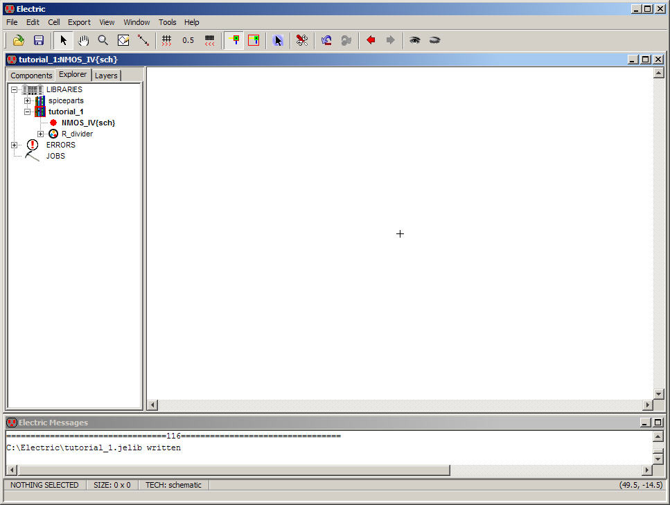
Notice
the R_divider group
from the
first tutorial is still present in this library.
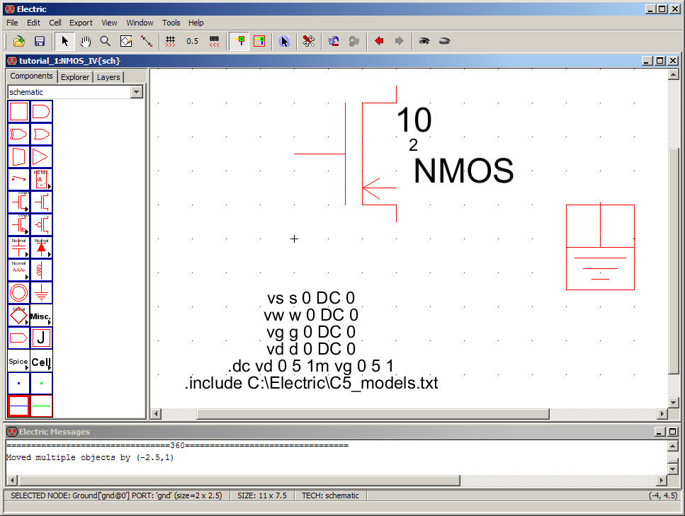
Next
go to the Components window and select/place the NMOS
Node, circled, as seen below.
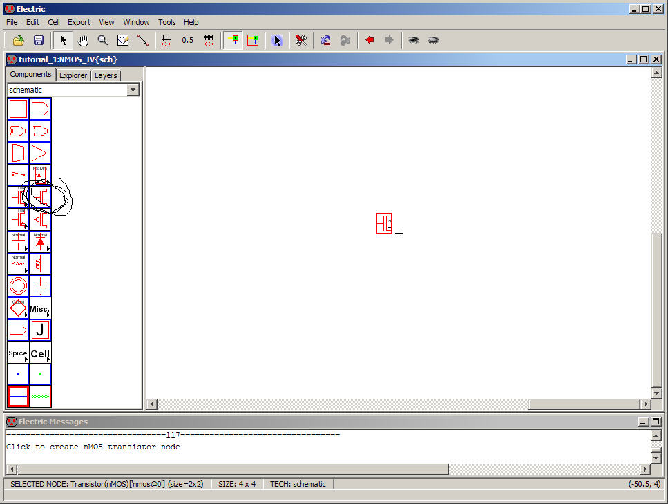
Fill
the window and then edit the Nodes properties.
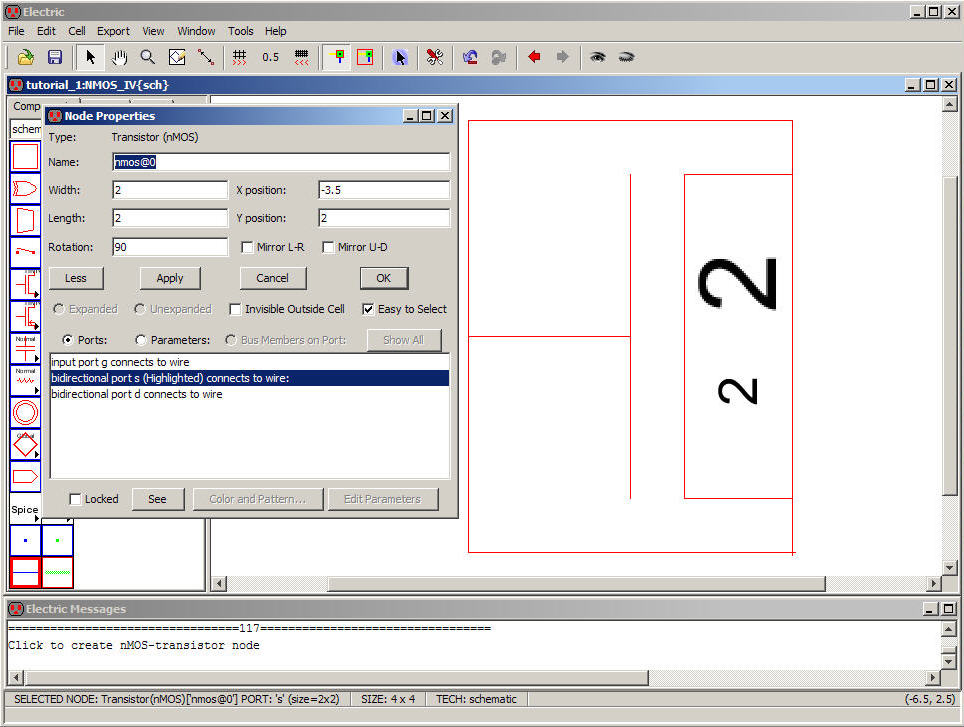
Let’s
set the width of the device to 10 and leave the length
at 2.
Hit
OK when finished.
Next
select (Ctrl-click is very useful for selection) the
text (the width and length) on the Node.
While
Nodes/Arcs can be rotated using Ctrl+J
or Edit -> Rotate text must be rotated via its properties as
seen below.
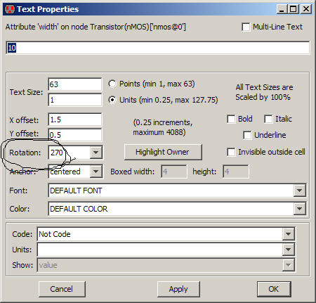
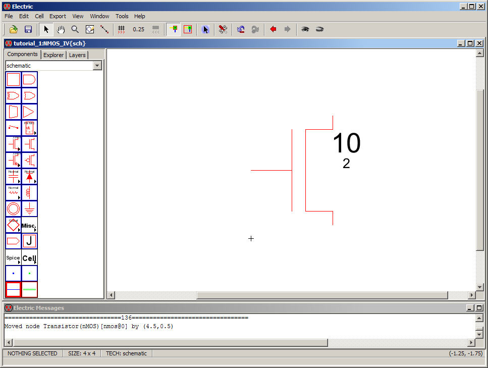
Rotate
and move both the width and length of the MOSFET until
you get the following.
Notice
how the grid alignment was reduced to 0.25 so that the
device’s length (here 2) could be move slightly away from center.
Change
the grid alignment back to 0.5.
Next,
select the
NMOS Node (the symbol) and go to Tools -> Simulation (Spice)
-> Set Spice
Model.
We
get the following.
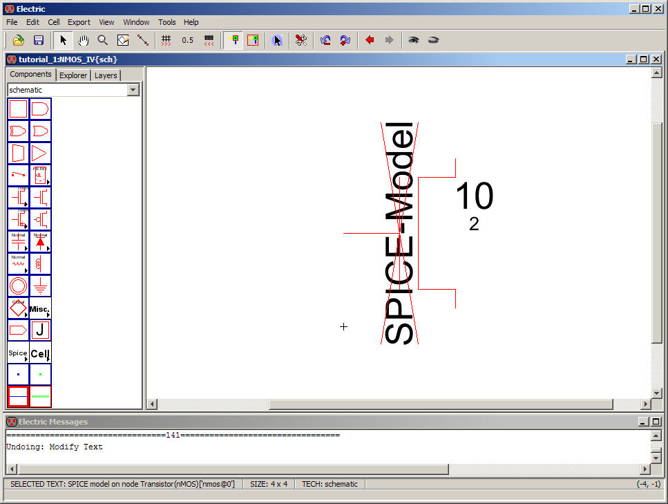
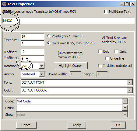
Edit
the SPICE-model text using Ctrl+I
From
the C5_models.txt file above we see that the NMOS model
name is NMOS and the PMOS model’s name is PMOS (easy to remember).
Change
the name to NMOS and Rotation to 270 as seen below.
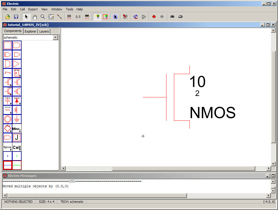
Move
the SPICE name to the position seen in the following.
From
this point on we can simply copy this Node to avoid
going through these steps every time we place an NMOS device.
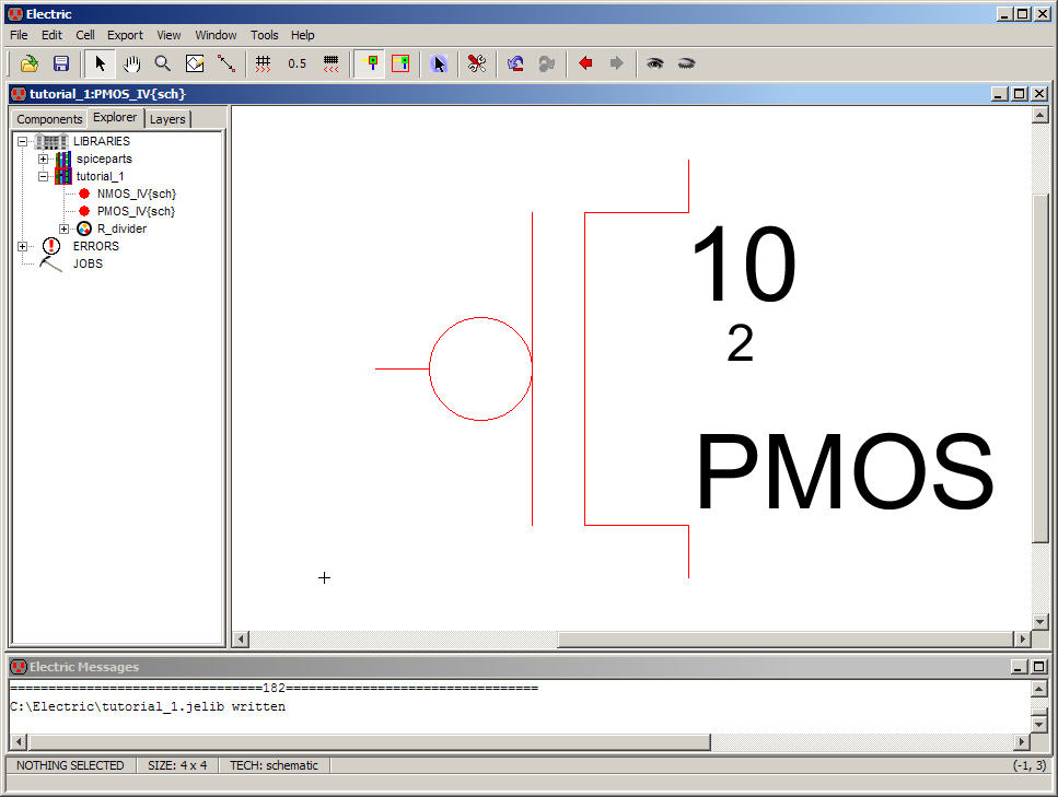
Repeat
these steps for the PMOS device.
The
cell name should be PMOS_IV.
The
result is seen below.
These
symbols are useful for general design but in this
tutorial we want to have access to all of the transistor’s terminals
including
the device’s body.
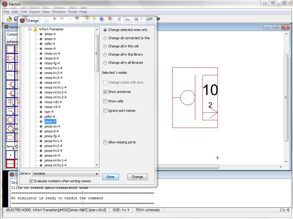
In
this PMOS_IV cell select the PMOS Node then go to the menu
Edit -> Change or simply press C (the corresponding bind key).
The
Window seen below will pop up.
Change
the Node to a 4-port device as seen (hit Apply then
Done).
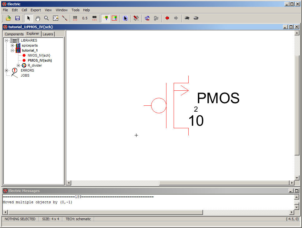
Notice
that the body (here the n-well) is next to the source
of the PMOS device.
Since
it’s common to draw the body and source at the top of
the device, for a PMOS, and the drain and the bottom let’s use Edit
->
Mirror -> Up <--> Down to flip the device so the
source/body are at
the top of the symbol.
Below
we’ve also moved the PMOS SPICE model name.
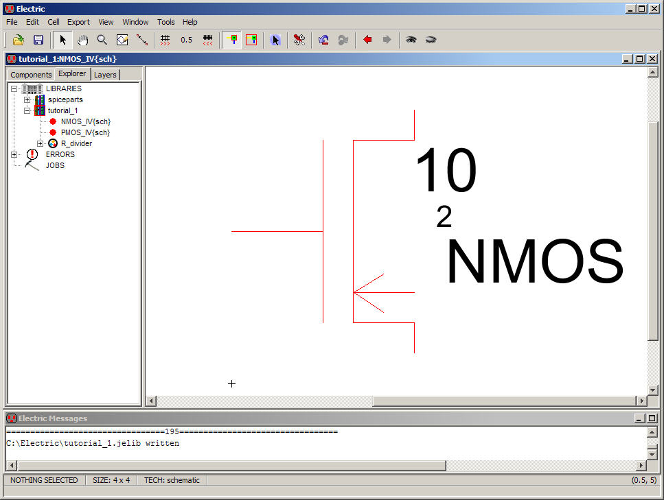
Let’s
repeat this (except for Up <--> Down mirroring)
for the NMOS_IV cell.
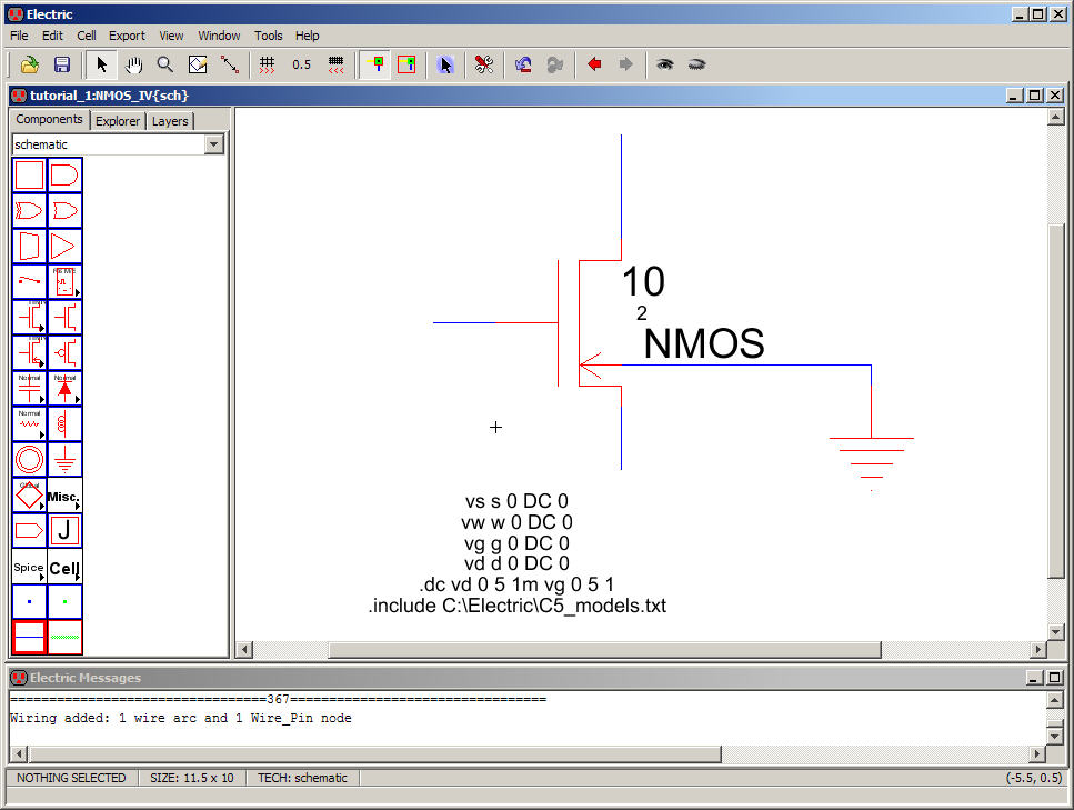
Next
let’s make layout views for these cells. Create these
two cells now (Cell -> New Cell)
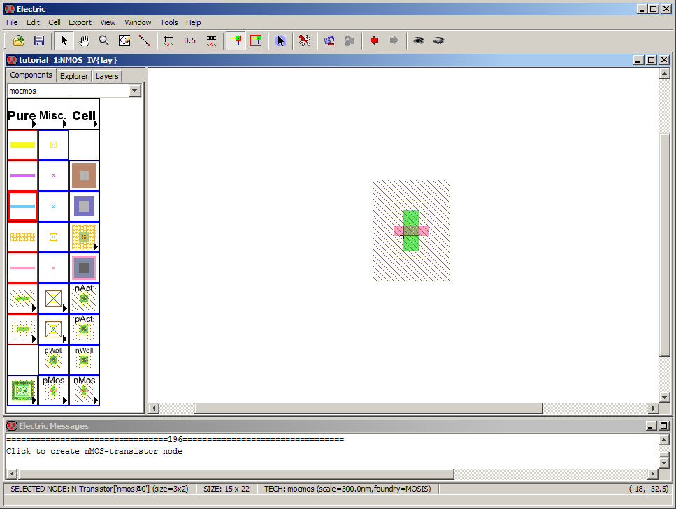
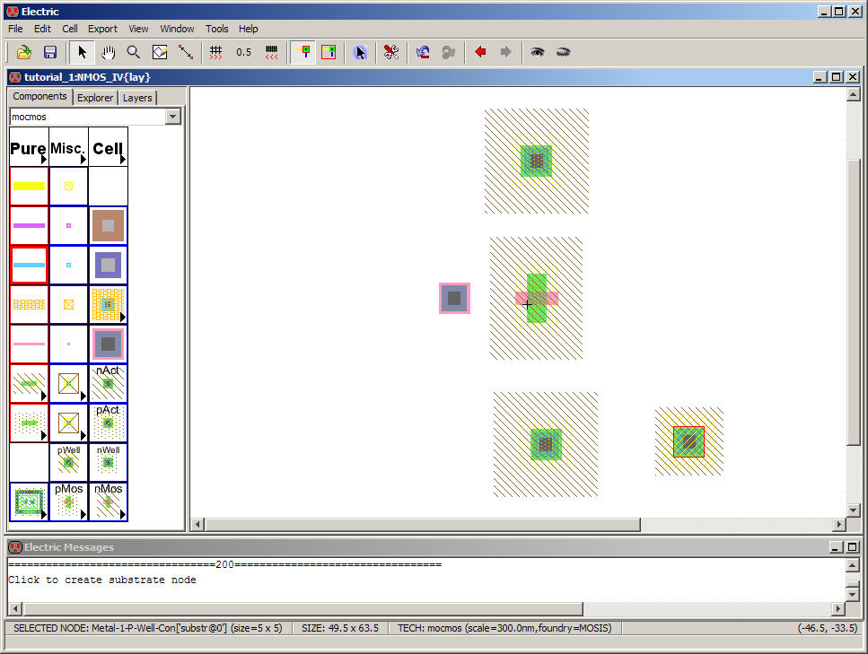
Go
to the NMOS_IV{lay} view as seen below.
Go
to the components menu on the left and select/place the nMos Node in the lower right
corner of the menu, as seen
below.
This
is the layout of an NMOS device consisting of a p-well,
active, n-select (to dope the active n-type), and poly (the pink).
Notice
the highlight box indicating the Node is selected.
Next
add nAct Nodes as seen
below.
These
will connect to the MOSFET to form the source and drain
of the device.
They
also provide a connection for metal1 Arcs to the MOSFET
S/D.
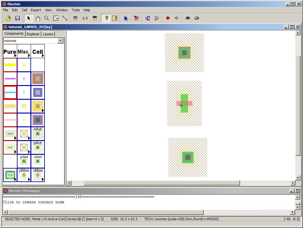
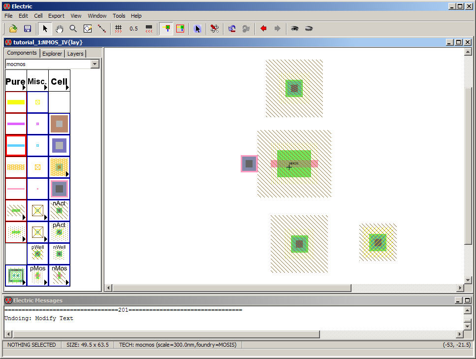
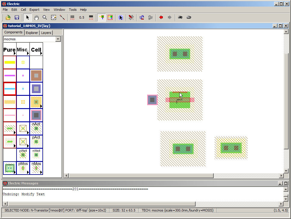
Next
add the metal1 to contact to poly1 as seen below.
This
Node is used for connecting metal1 to the MOSFET’s gate
terminal.
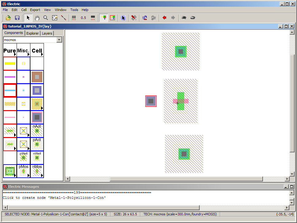
Finally,
let’s place the body connection for the NMOS device,
the pWell Node seen
below.
Zoom
out as needed.
We
are now ready to connect the Nodes together with Arcs.
To
size the Nodes use Edit -> Properties -> Object
Properties (Ctrl+I or,
if you have my Key Bindings
from the first tutorial, just press lowercase Q)
Go
to the nMos Node and
change its
Width to 10.
Next,
with the nMOS Node
still
selected, go to Tools -> Simulation (Spice) -> Set Spice
Model… and set
the SPICE model name to NMOS (if you don’t do this we can’t simulate
the
layout)
The
result is seen below.
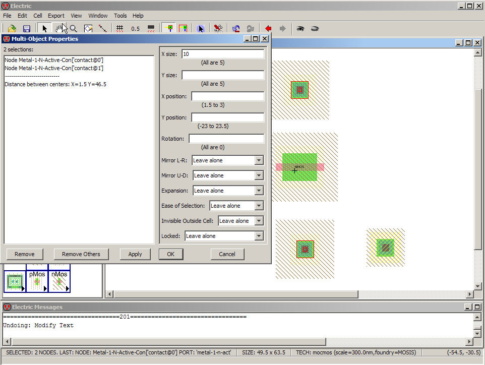
Next
select both of the nAct
Nodes.
To
select both first select one and then, while holding down
on the Shift key, select the other.
Edit
their properties and the following Window will open.
Change
the X size to 10, the same width as the MOSFET.
Note
that you can change each nAct
Node individually but we want you to learn the tool so you can do
things
quickly ;-)
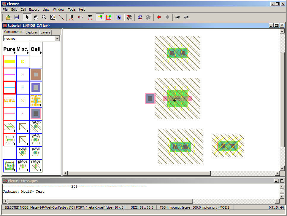
The
last step, before wiring the Nodes together, is to change
the X-size of the pWell
Node.
Let’s
set the width to 10 as well, see below.
Next,
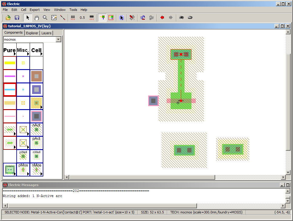
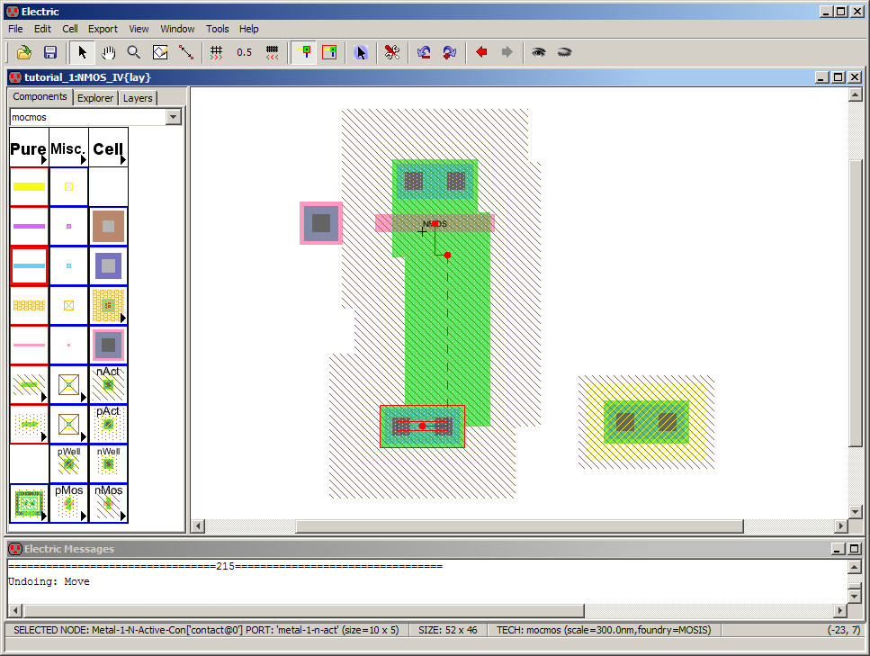
using the left mouse button select the top port on the nMos Node as seen below.
Move
the mouse up to top nAct
Node
and RIGHT click on it.
The
result is seen below. An N-Active Arc was added between
the Nodes.
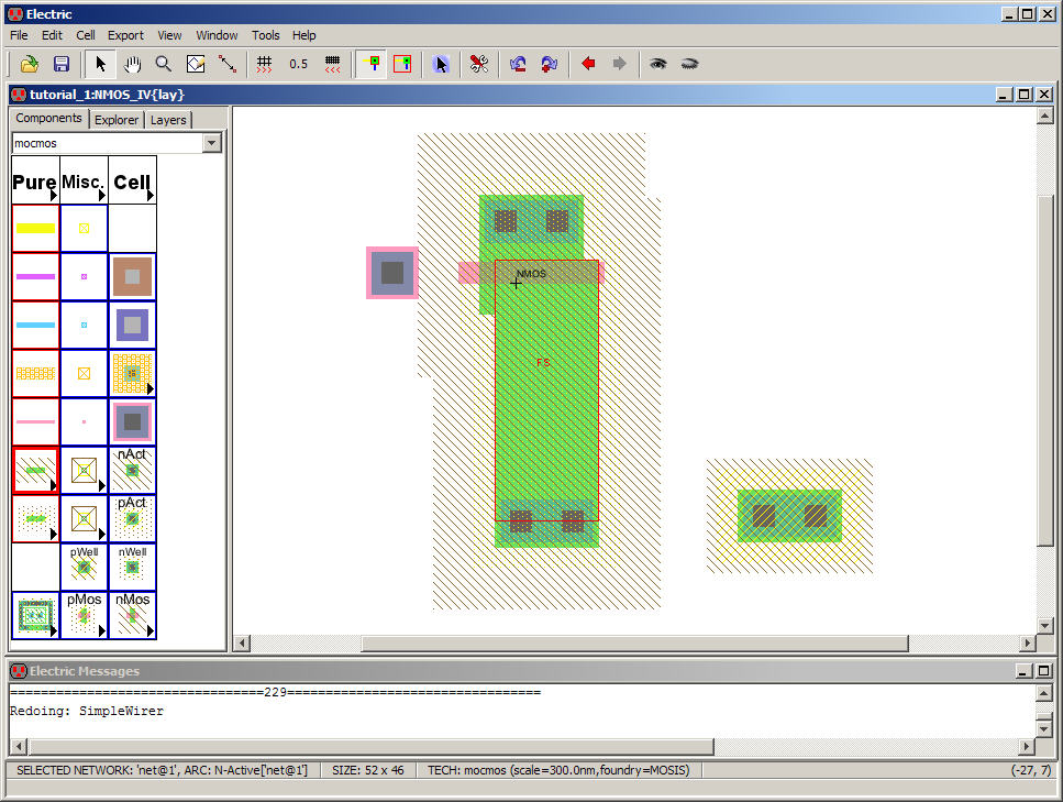
At
this point move the nAct
Node
down to match the following.
DRC
your layout, F5, after you’ve moved the Node to ensure no
design rule errors.

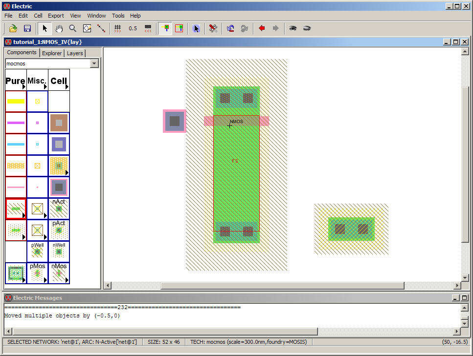
Next
let’s show what would happen if we had selected the nAct Node first, see below.
Moving
the cursor up and RIGHT clicking on the nMos
Node results in the following.
Notice
that the width of the Arc changed and that both ends
extend beyond the red dots.
If
we select the bottom nAct
Node
and move it to the left we get the following.
If
we keep moving this Node the n-Active Arc will eventually
move as well.
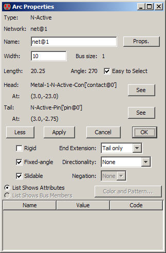
This
behavior is related to the Arc’s properties, see below.
Selecting
Rigid will make the Arc move when we move the nAct
Node.
Pressing
Ctrl+Z (undo) until we
get
back to the point where we just added the N-Active Arc and then
selecting this
Arc results in the following.
Notice
how the Arc extends beyond the poly1 (the pink).
This
is an issue that will cause design rule errors (Active
spacing error). We’ll discuss in greater detail shortly.
With
this Arc active use the left arrow to move the Arc over
until it aligns with the nMos
Node, see below.
Instead
of using the arrows you can use the mouse to move the
Arc over. Notice the bottom nAct
Node moves too.
Move
the bottom nAct Node up
into
place (mirror of the top nAct
Node) and DRC the
layout.
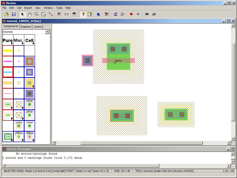
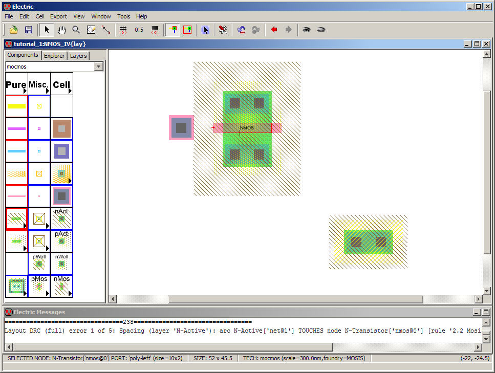
There
are 5 DRC errors. Pressing the > key we get the
following, that is N-Active TOUCHES the transistor Node.
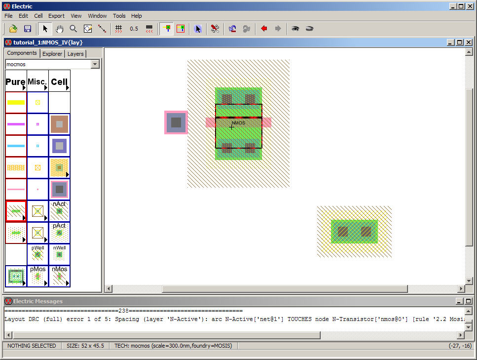
To
fix this error select the bottom N-Active Arc as seen
below.
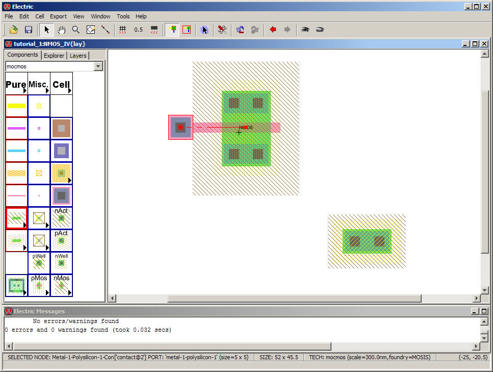
It
may be useful to press Ctrl+click
to cycle through the possible selections.
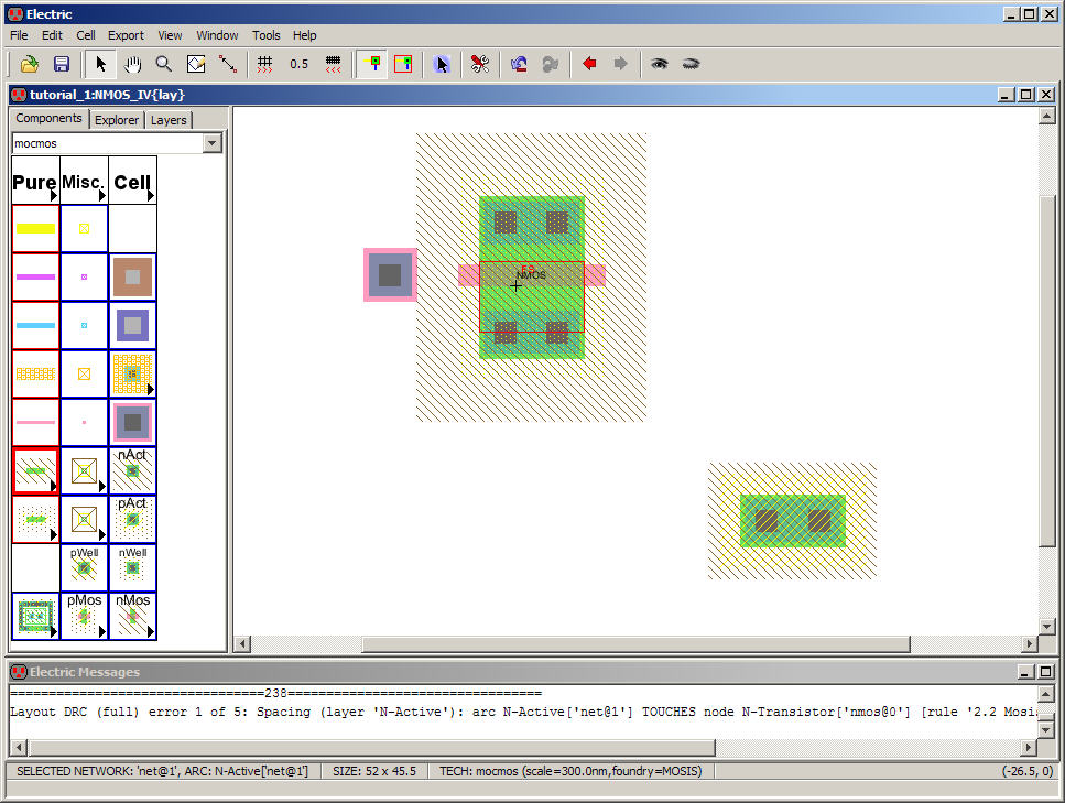
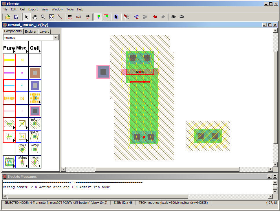
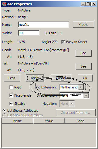
Change
this Arc’s properties (Ctrl+I)
so that the End Extension is “Neither end” as seen below.
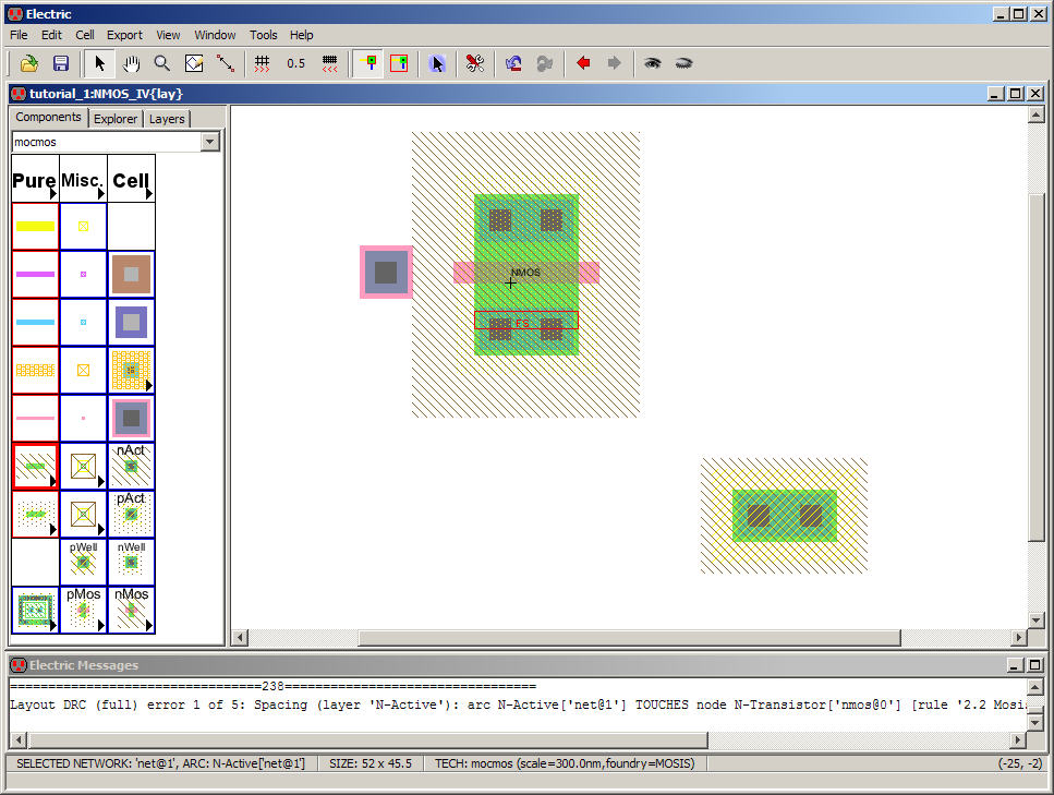
The
result is seen below. Now the layout passes DRCs.
Let’s
connect the gate of the MOSFET to the poly1 to metal1
contact Node by first selecting the left poly1 port on the transistor,
as seen
below.
Moving
the cursor over to the metal1-poly1 contact and RIGHT
clicking gives the following.
DRC
the resulting layout to verify no DRC errors.
Let’s
not forget about the ERC Well Check (Tools -> ERC
-> Checks)
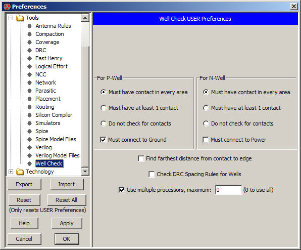
To
view the related setups go to File -> Preferences ->
Tools -> Well Check to see the following (setup from Tutorial 1)
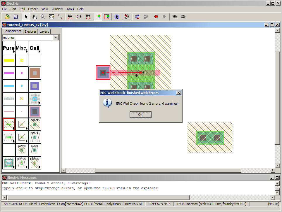
When
we perform a Well check on the above layout we expect to
get two errors:
one
because there is no well contact in the p-well
surrounding the NMOS device and
a
second because the isolated pWell
Node isn’t connected to ground, see below.
Moving
the pWell Node over so
that
it overlaps the nMOS
p-well layer, as seen below,
takes care of the first error.
Perform
a DRC and ERC well check after moving this Node to
show no DRC errors and only a single ERC error.
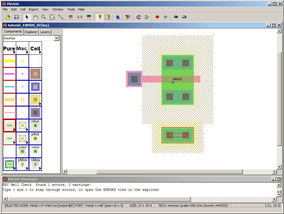
To
let Electric know that we are going to only connect the
substrate to ground, move your cursor below the selected pWell
Node and RIGHT click to get the following.
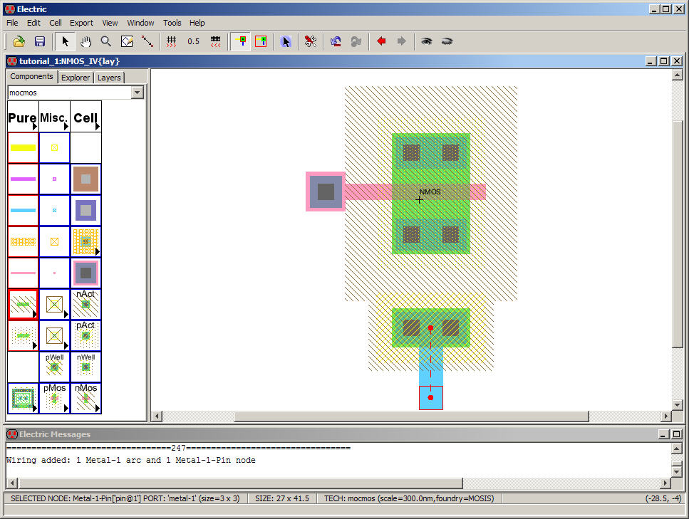
At
this point you should know how to select the added metal1
Arc above and how to change its width and end extension.
What
we are going to do is “Export” the connection to the
p-substrate via the pWell
Node and the metal1 Arc we
just added.
Only
Nodes can be exported so we can’t export the metal1 ARC.
This
means that we can Export the highlighted Pin above or
the pWell Node.
Let’s
export the Pin seen above. If it’s not highlighted then
use Ctrl+click until
the Pin is selected.
Next,
with the Pin selected, go to the menu and select Export
-> Create Export (or just use Ctrl+E)
Set
the Export name to “gnd”
as
seen below. Leave the Export characteristics at unknown.
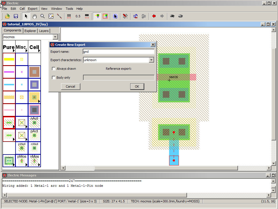
It’s
important (when we do an NCC) to use lowercase gnd
to represent ground (to match the symbol we’ll use for
ground in a schematic shortly).
We’ll
also use lowercase vdd
to
make the power symbol NCC (aka LVS) correctly.
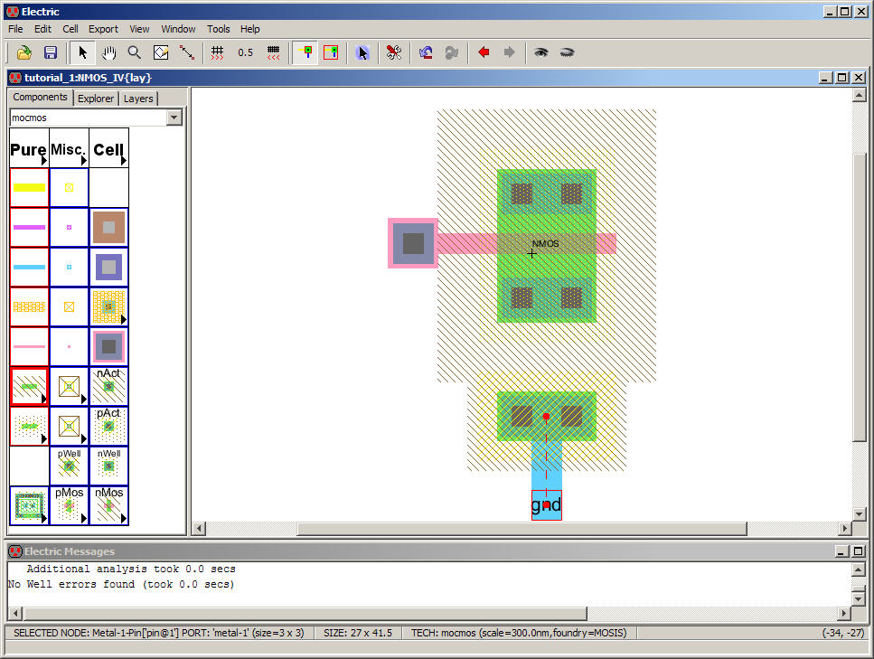
The
result is seen below. Now when we perform a well check we
don’t get errors (see Electric Message window below).
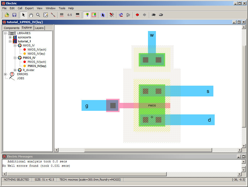
Let’s
add metal1 Arcs for the other 3 MOSFET terminals and
export as seen below.
Make
sure to DRC and ERC-Check Wells when you are done.
Also
ensure you are exporting the Pins of the metal1 Arcs.
If
you try to add an Arc connection to the S/D regions and
N-Active Arcs are used go to the menu and select metal1, which is
circled
below.
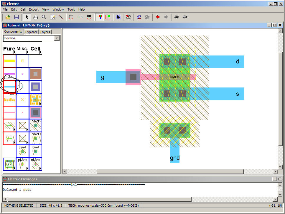
Save
your library, tutorial_2.jelib.
We
can follow the same sequence of actions to lay out the
PMOS_IV cell.
Let’s
provide an abridged set of instructions to speed things
up.
Go
to the PMOS_IV{lay} view cell and add the Nodes seen below
(labeled with Annotation text found in the Misc menu)
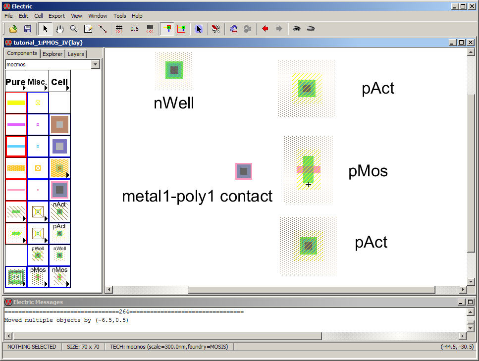
Change
the width of the nMos
Node
to 10 and the x-size of the remaining Nodes to 10 with the exception
the
metal1-poly1 contact Node.
Next
select the pMos Node
and go to
the menu, Tools –> Simulation (Spice) -> Set Spice Model…
and set the
PMOS’s SPICE model to PMOS.
Important
if we want to simulate the layout (and we do!)
The
result of these actions is seen below where the SPICE
model name has been circled since it’s hard to see.
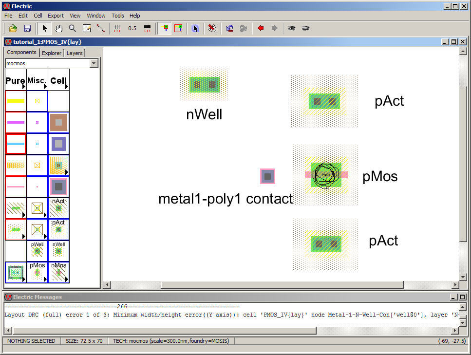
If
we perform a DRC check on this layout we get the following
error (the nWell isn’t
tall enough).
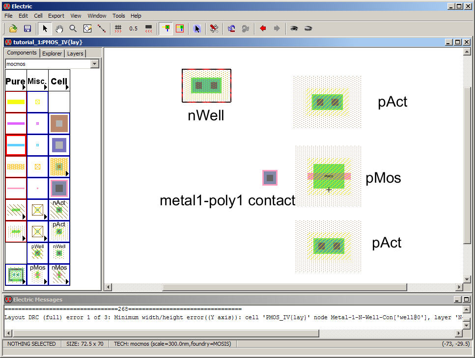
Change
the y-size of the nWell
Node
so that it’s 6.
You
may have additional well errors if you’ve placed your
Nodes too close together.
All
of these errors disappear after the Nodes are connected
together.
Let’s
connect them together now, export the Pins, and delete
the Annotation text as seen below.
DRC
and ERC Well Check your design.
There
shouldn’t be any errors.
Note
that we could add some confusion by naming the Arcs (d,
g, s, and w) above (by selecting the Arc and editing its properties
using Ctrl+I) instead
of exporting the Pins at the end of the
Arcs.
This
may sound silly now but when you get going fast, and are
used to naming Arcs so that simulation data is easier to view (so you
know what
you are probing), this is a common mistake.
We
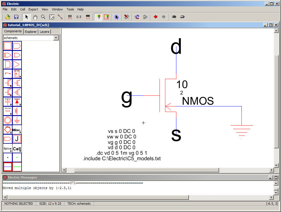
are ready to simulate.
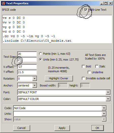
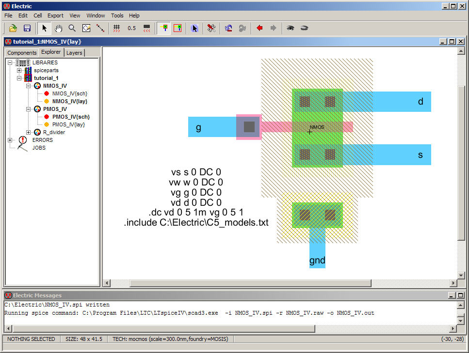
Go
to the left Component menu and select the arrowhead under
Misc to access Spice Code.
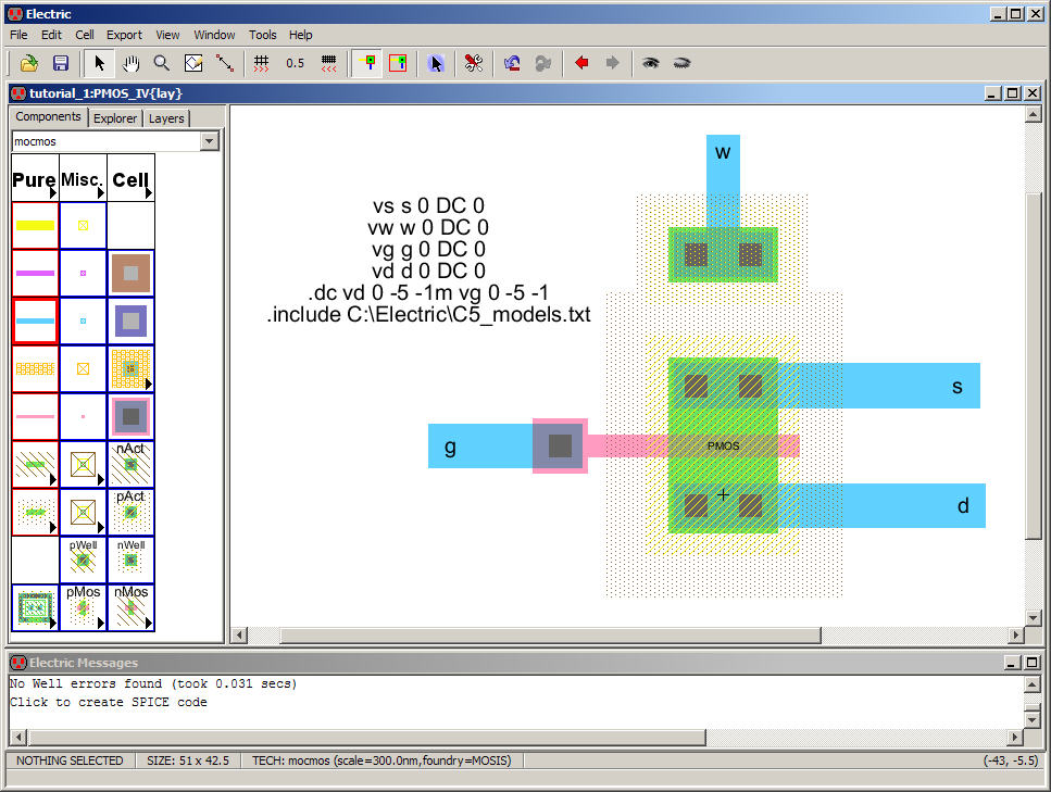
Add
the Spice code seen below while ensuring you are using
multiple lines and the text size is increased to 2.
The
cell now looks like the following.
Note
that if you haven’t saved the C5 models to C:\Electric
as discussed at the beginning of this tutorial the simulation we’re
about to do
won’t run (correctly).
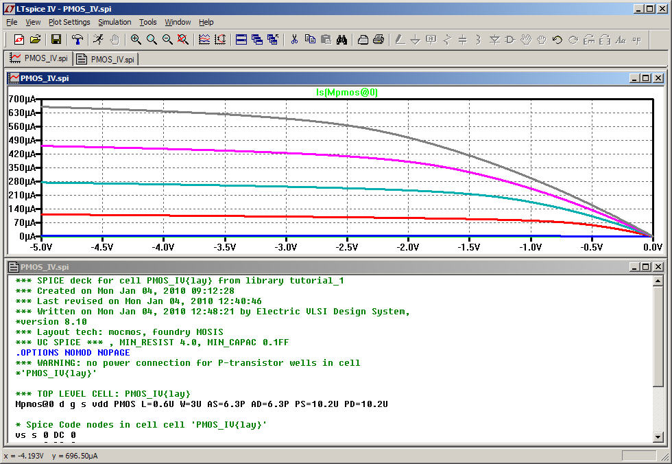
Going
to the menu Tools -> Simulation (Spice) -> Write
Spice Deck
results
in the following (again, assuming, as mentioned in
Tutorial 1 that you have LTspice setup correctly) when you plot the
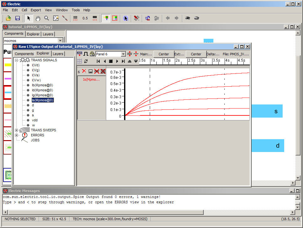
source
current of the PMOS device
or
using Electric’s probe which should run after you’ve
closed LTspice (of course you have to use the Explorer to select the
right
signals).
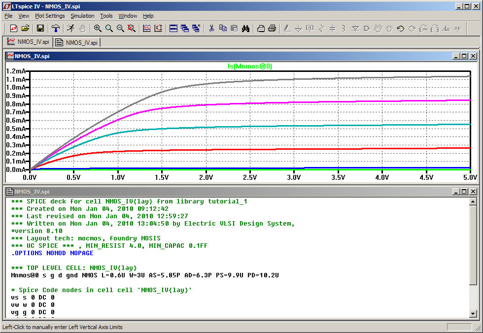
Adding
similar Spice Code to our NMOS_IV{lay} view results in
With
simulation results from LTspice
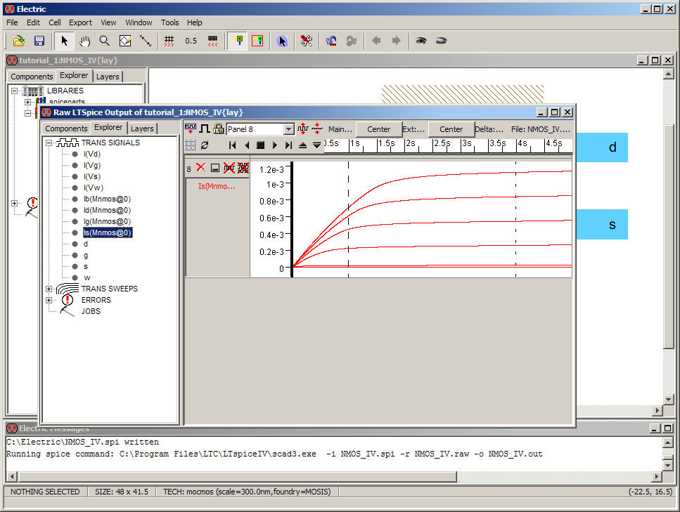
and
using Electric’s probe
The
last step is to finish up the schematics so the layout
and schematic NCC without errors.
Copy
the Spice code from NMOS_IV{lay} to NMOS_IV{sch}
and change the text’s size from 2 to 0.5.
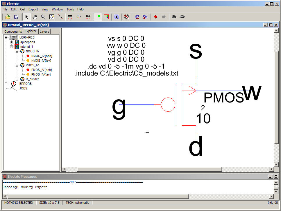
Repeat
for the PMOS_IV cells.
Go
back to the NMOS_IV{sch}
cell
and select/place the ground symbol from the Component menu on the left,
see
below.
The
ground Node symbol is a little large, relative the MOSFET
symbol, so let’s shrink it.
First
turn the Grid on by pressing Ctrl+G
or Window -> Toggle Grid
With
this ground Node active go to Edit -> Size ->
Interactively or just press Ctrl+B
Adjust
the size so that the ground Node is smaller and its
single port at the top of the symbol stays on Grid, see below.
Next
turn off the grid and add wire Arcs to get the
following.
We
need to export Pins to make the schematic/layout NCC
correctly
To
see the Pins let’s draw a box around everything, as seen
below.
If
this doesn’t work make sure that you have the Select
Objects button (circled below) enabled (not the Select Area)
Using
Export -> Create Export (or better yet Ctrl+E)
export the appropriate Pins to match the layout,
see below.
Remember
to use Ctrl+click for
ease
of selection.
Make
sure, as in all of these tutorials, that you leave the
Export Characteristics at “unknown”
Note,
again, we could confuse ourselves if we named the Arcs
with these names instead of Exporting the Pins
Verify
the above schematic matches the layout (perform an
NCC)
At
this point you can also simulate this schematic (since
this is easy go ahead and do it).
Repeat
these steps for the PMOS schematic view.
The
end result is seen below.
Again
verify that this schematic matches the layout using
NCC.
Also,
again, this schematic can be simulated (go ahead and do
this).
This
is the end of the second tutorial.
For
your reference the final jelib
(Electric library)
used in this tutorial is located in tutorial_2.jelib
These
first two tutorials have covered most of the basics of using Electric.
We
are now ready to design, layout, and simulate more complicated CMOS
circuits.