Electric
VLSI Design
System
Tutorials
from CMOSedu.com (Return)
Tutorial
6 – Placing circuit layouts in a padframe
for
fabrication
In this tutorial
we’ll take the circuits we designed in the previous tutorials and place
them on
a simple padframe for
fabrication.
To begin this tutorial, use Electric to open the jelib we created in tutorial 5, tutorial_5.jelib (right click to save to C:\Electric).
Save this library
as tutorial_6.jelib, again in C:\Electric.
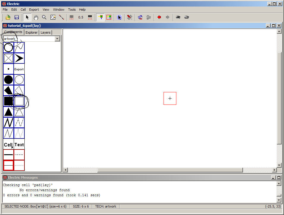
Create
the layout view of a cell called “pad.”
Go
to the artwork menu and select/place a Box as seen below.
Our
setups were created in Tutorial
1 using in On Semiconductor’s C5
process and
fabrication through MOSIS.
Further,
this process uses the MOSIS scalable CMOS (SCMOS) submicron design rules.
A
tiny chip fabricated in this process via the MOSIS Educational Program
(MEP)
measures 1.5 mm by 1.5 mm.
Information
about the MOSIS Educational Program (MEP) is found here.
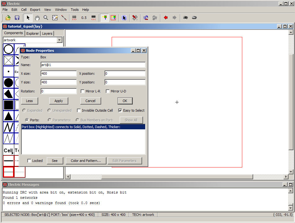
We
need to determine the size of the Pad cell above.
The
scale factor (lambda) used in these setups is 300 nm so a layout that
measure
5000 by 5000 is 1500 um by 1500 um (1.5 mm = 1500 um)
If
we have 12 cells on a side (10 plus two corners) then each cell must be
5000/12
or 416.66.
We’ll
round this down to 400 to ensure our chip is a little smaller than the
maximum
size of 1.5 mm square.
Change
the size of the Box above to 400 square and center it on 0,0 as seen
below.
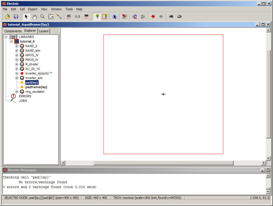
Before
we add anything to our pad cell let’s create a layout view of a padframe cell (do this now).
Place
the pad cell into this padframe
cell as seen below.
Next
let’s use the Array command (Edit -> Array or simply F6) with
the pad cell
selected.
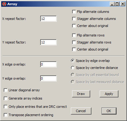
After
filling the window we get the following.
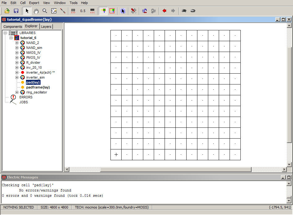
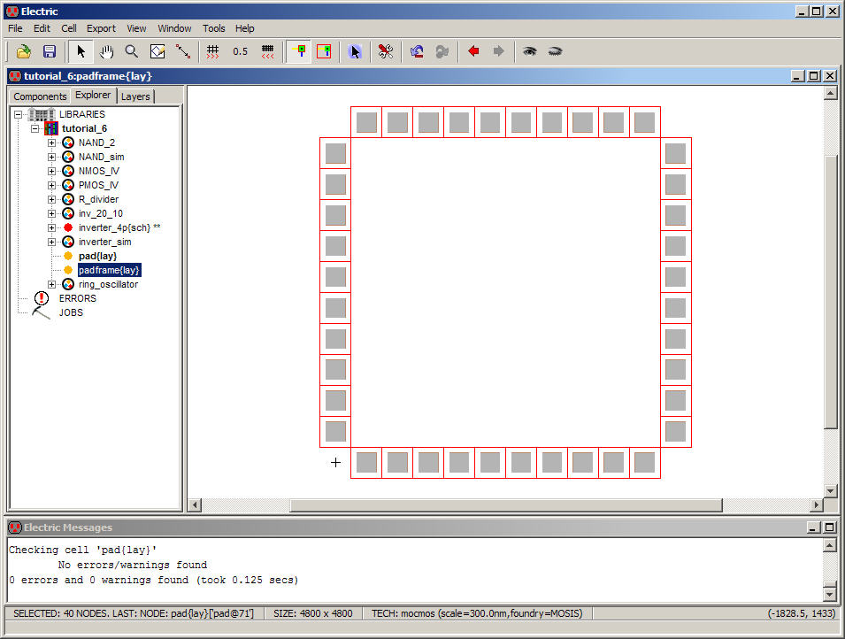
Next
delete the corner and interior pad cells.
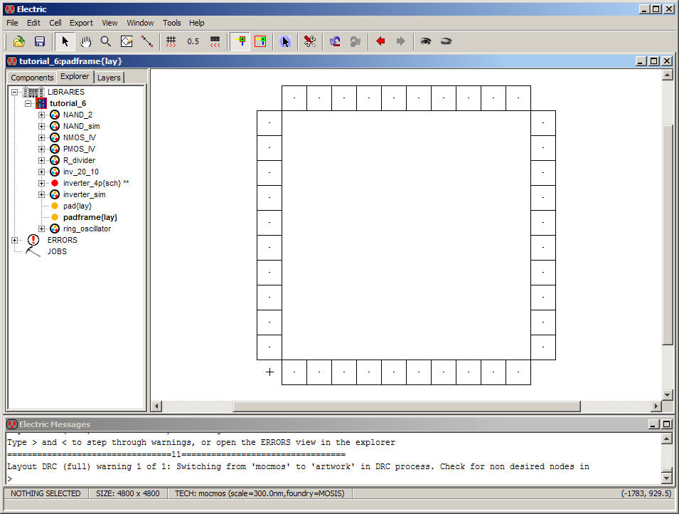
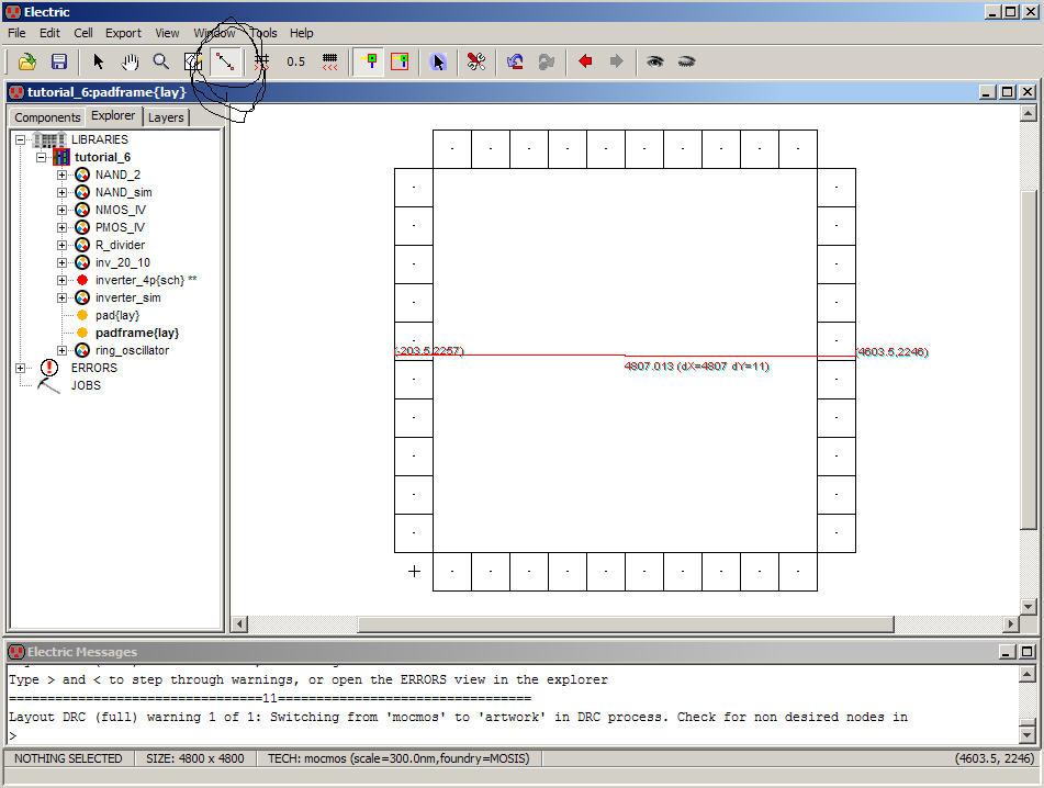
Let’s
measure the size of the cell using Windows ->
Measurement -> Toggle Measurement Mode (or press M or use the
circled icon
seen below)
Pressing
M toggles back and forth between making measurements
and the normal click/zoom/wire cursor.
Pressing
Esc (or Windows -> Measurement -> Clear
Measurements) while in the measurement mode clears the measurements.
Note
that the exact size of the cell, 4800 by 4800, is seen
at the bottom of the display.
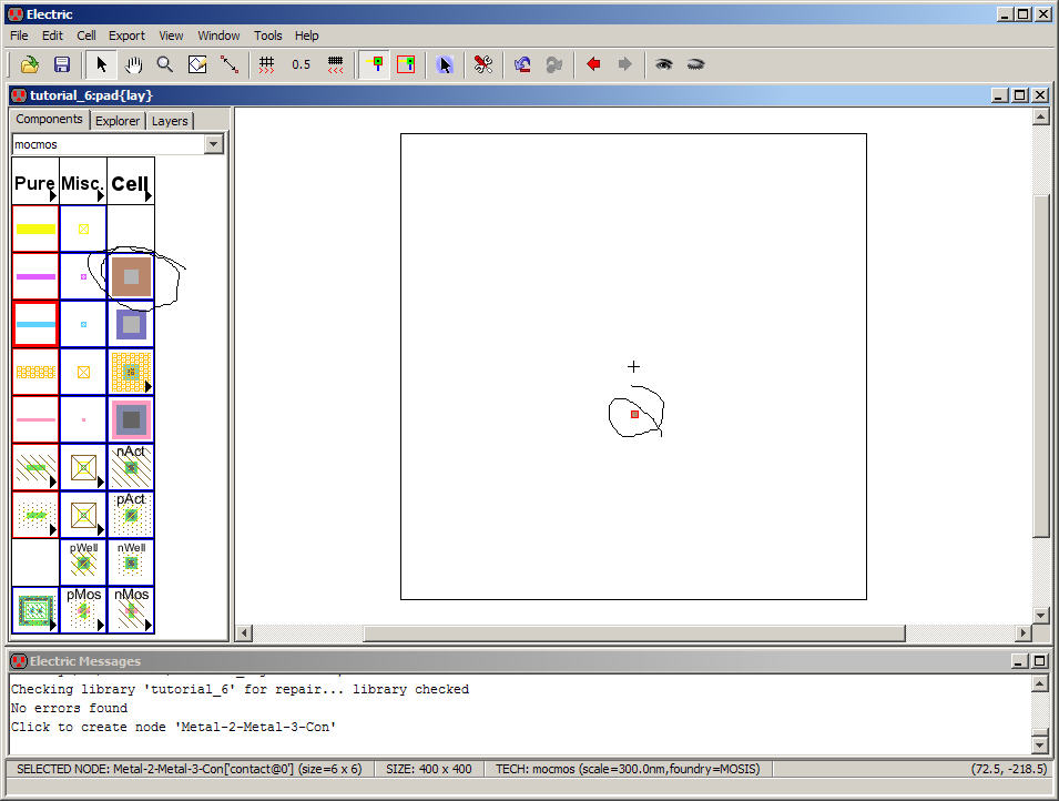
Let’s
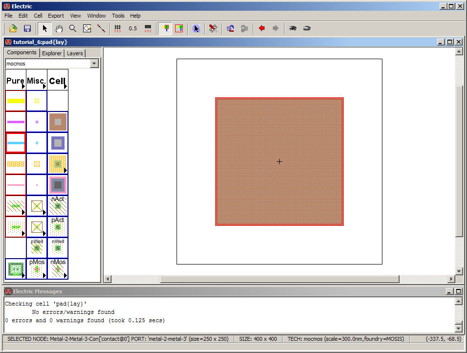
go back to the pad cell and add metal to make the pad.
We’ll
using 75 um square bonding pads so, since the scale
factor is 300 nm, a 250 lambda square piece of metal is used.
Add
a metal2-metal3 contact Node to the pad layout as seen
below.
Change
the size of this Node to 250 by 250 and center it on
0,0 as seen below.
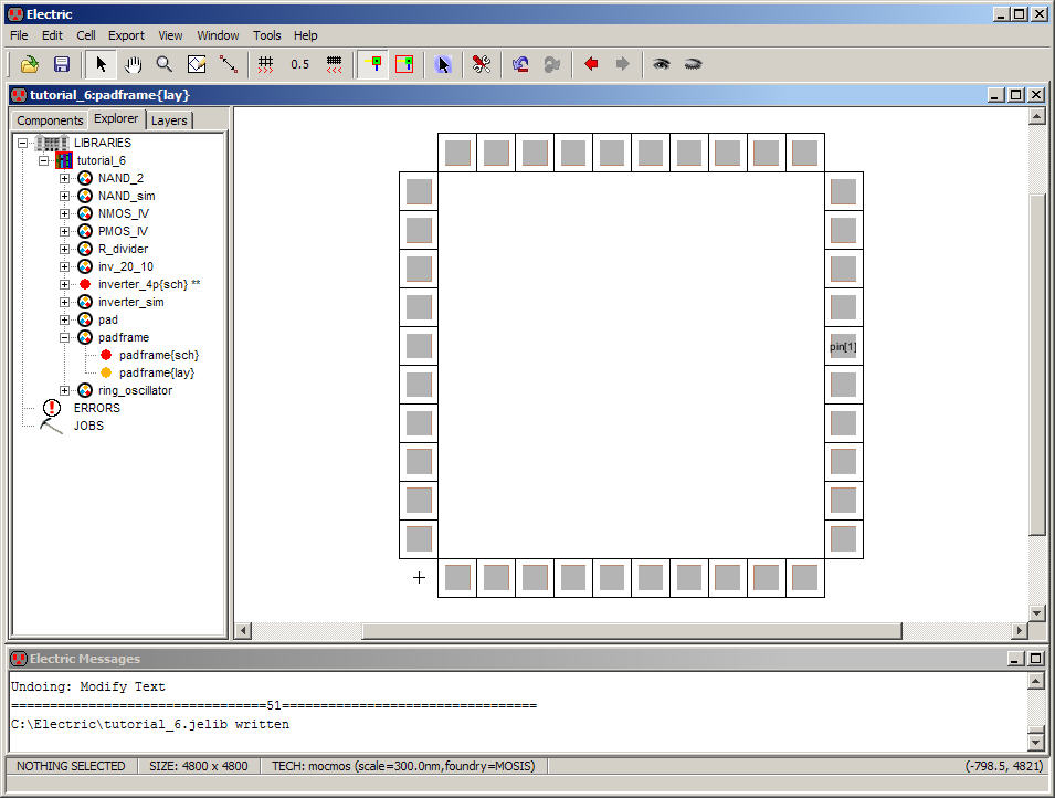
Our
padframe now looks like
the
following (after selecting the cells and using the open-eye on the menu
to show
the cells’ contents).
Let’s
go back to the pad cell.
We
need to do two things to this cell, add an Export so that
we can connect to it, and
add
the Passivation layer
(sometimes called overglass)
so that the top layer of
passivation (glass) is
removed
and get access to the metal3 (else we can’t get the
signals off chip!).
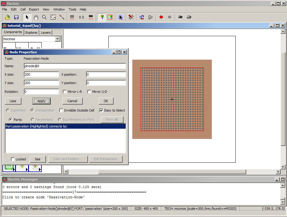
According
to the design rules the minimum overglass
opening is 60 microns (200 with our 300 nm scale factor).
Add
a Pure layer of Passivation
to
the pad cell.
Next
change the size of this Pure-Node to 200 by 200 and
center it on 0,0 as seen below.
Next
select the metal3-metal2 Node and Export it as inout.
Change
the size of the Export text to 25 as seen below.
DRC
your design to ensure no errors.
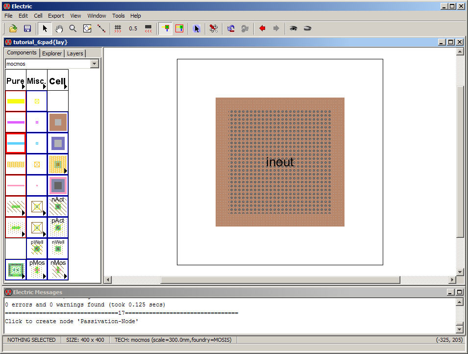
The
layout of our pad is complete.
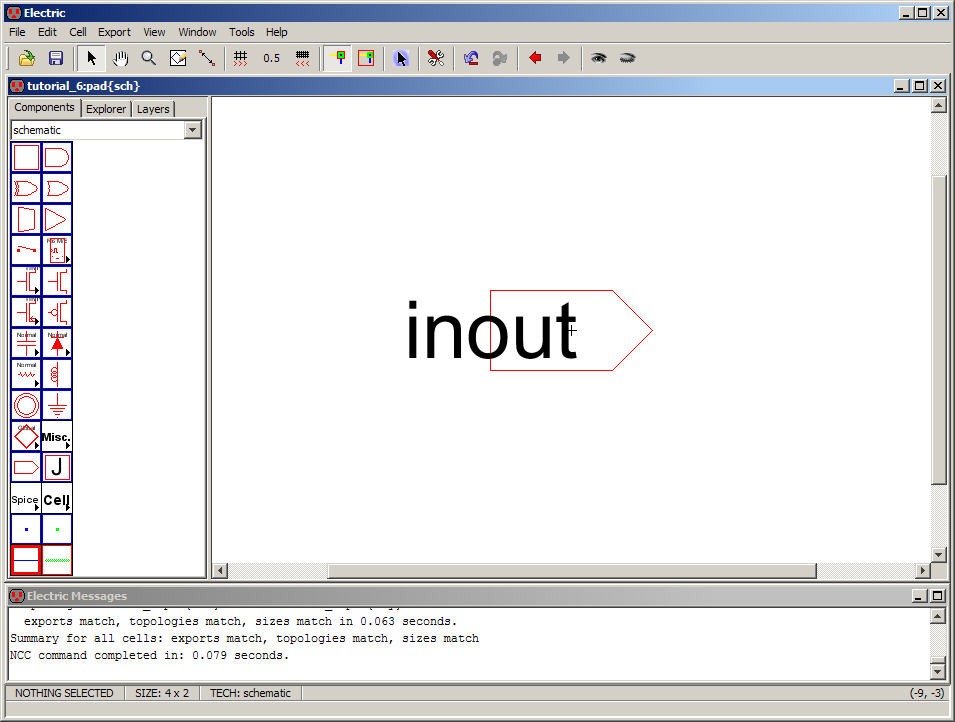
Let’s
now make a schematic representation for this layout.
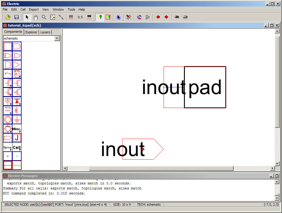
Create
a schematic view of the pad cell.
Add
the off-page Node and Export inout
as seen below.
Check
the schematic (F5) and NCC the layout and schematic
views.
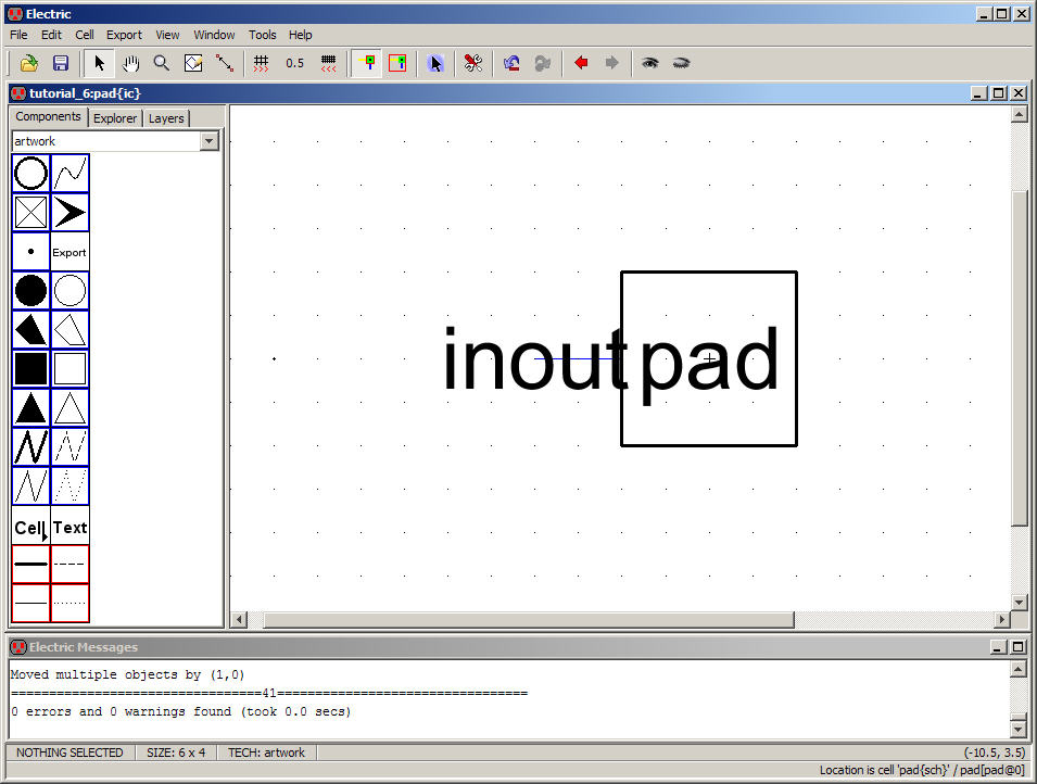
Next,
go to View -> Make Icon View
Descend
into the icon.
Select
the box and use Edit -> Modes -> Edit ->
Toggle Outline Edit (or just press Y) to adjust the size of the box.
When
finished adjusting the size press Y to get out of this
mode.
Adjust
the sizes until you get something that looks like the
following.
The
schematic view of the pad now looks like the following.
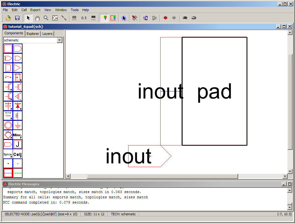
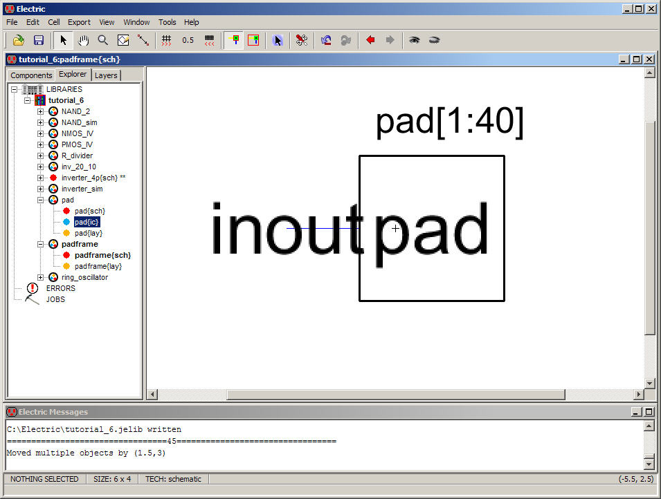
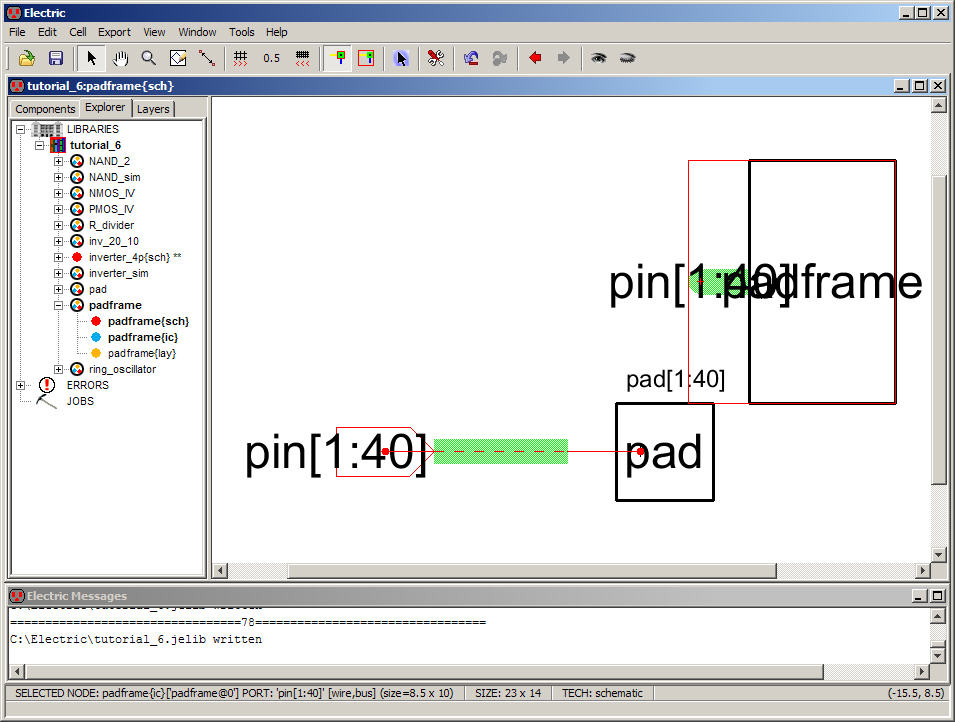
Let’s
create a schematic view for the padframe
(do this now).
Place
the icon of the pad into the schematic view of the padframe cell and
change
its name to pad[1:40] (and move the name) as seen
below.
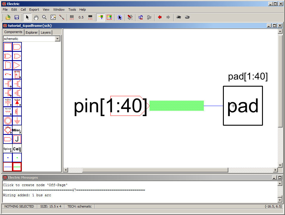
Next
add an off-page Node and connect a bus between the pad
icon and the off-page Node.
Export
the port of the off-page node as seen below using the
name pin[1:40].
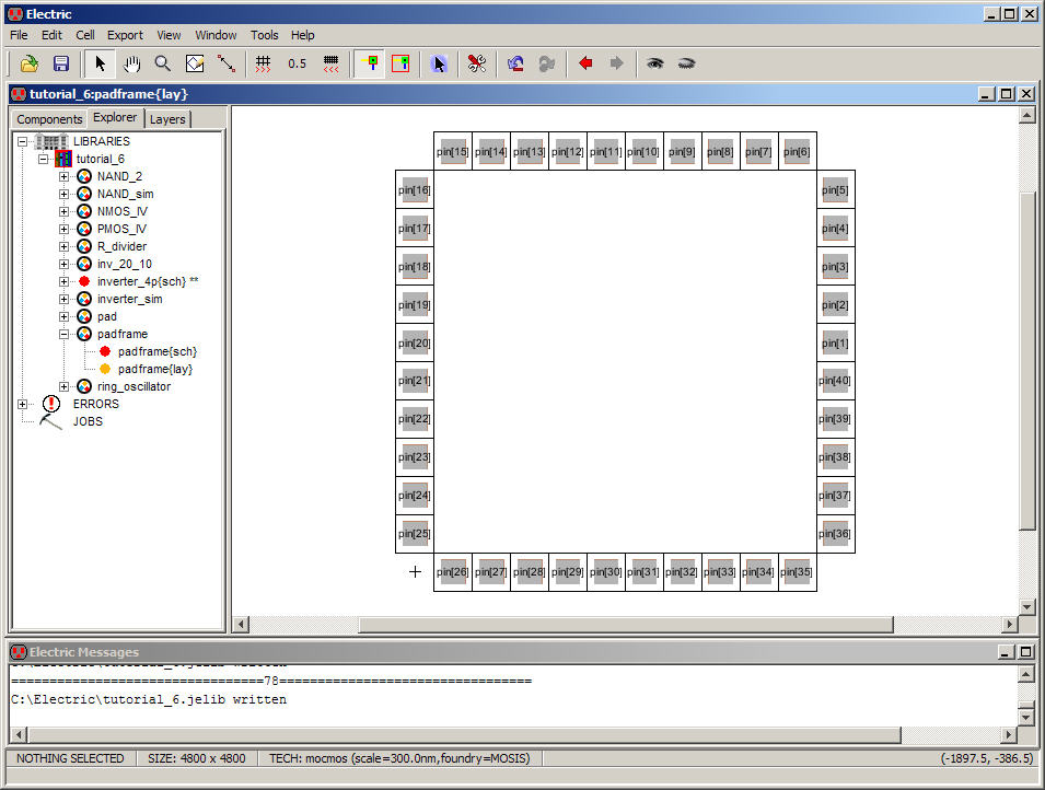
We
haven’t exported anything in the padframe
layout so we need to go back and do that.
However,
it would be nice if pin[1] corresponds to pin1 of
the package.
MOSIS
uses a 40 pin DIP package for the educational program
with a bonding diagram seen
below
(our padframe, that is,
chip
is in the middle of the figure).
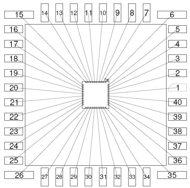
Pin1
of the package is connected to the fifth pad from the
top and the right side.
Let’s
export this pin on the padframe
layout now (and change the export text size to 125).
We
need to do this for the other pins.
One
trick, after you’ve exported all the pins is to select
the entire layout, then Ctrl+I
it
and removing everything but the text. Then change the text
unit size to 125.
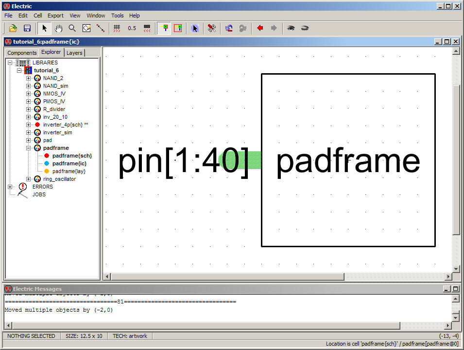
Next
let’s create an icon view for the padframe.
Go
back to the schematic of the padframe
and use View -> Make Icon View
Descend
into the icon view of the padframe
and use Edit -> Modes -> Edit -> Toggle Outline
Edit (or just press Y)
again to adjust the size of the box.
Move
the Export text to the left until you get something that
looks like the following.
Save
your library.
We
are now ready to make a cell for our final chip (the chip
we want to send out for fabrication).
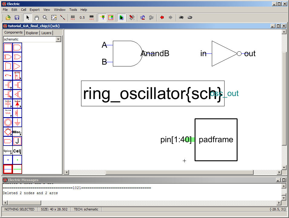
Make
a schematic view for a cell called A_final_chip.
This
name was selected so that the cell would be at the top
of the Explorer.
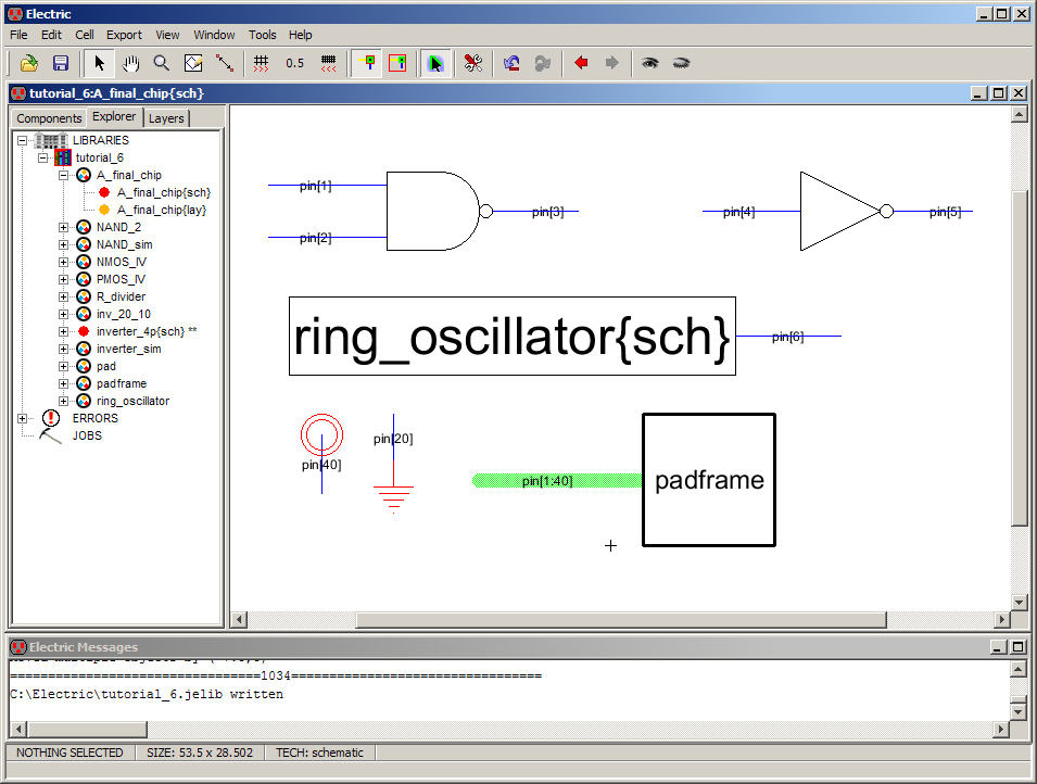
On
this chip we’ll place the NAND_2, inv_20_10, and the ring
oscillator.
Since
the two schematic views of the ring oscillator have
Spice Code in them let’s create a third version and remove the Spice
Code.
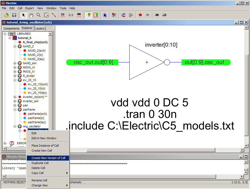
Since
the NAND_2 and inv_20_10 cells have icon views let’s
place the ring oscillator without an icon view.
Note
that we can easily make an icon (View -> Make Icon
View) but we aren’t just to be different.
Let’s
Export osc_out as seen
below.
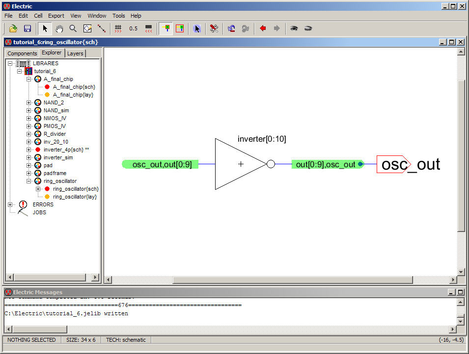
We
need to go to the layout and Export a Pin as osc_out.
We
also need to remove the Spice Code as seen below (feel
free to make a new version of the cell so you can go back and simulate
if
desired).
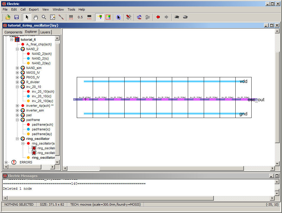
Verify
the resulting layout NCCs, DRCs, and Well Checks
without errors.
Open
the schematic view of A_final_chip.
In
this cell add the icon views for NAND_2, inv_20_10, the padframe and the schematic view
of the ring oscillator.
First
let’s connect a bus to the padframe
icon.
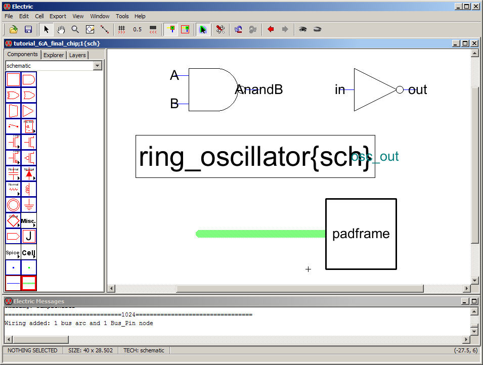
Next
let’s add wire Arcs to the icons and ring oscillator
then label the bus connected to the padframe.
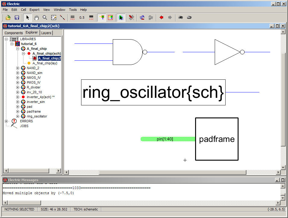
Let’s
connect the gnd and vdd to pins 20 and 40
respectively
Lets
connect A, B, and AnandB
to
pins 1, 2, and 3 respectively.
Inverter
in and out will be connected to pins 4 and 5
respectively.
Finally
let’s connect osc_out
to
pin 6
The
results are seen below.
Check
your schematic for errors (F5).
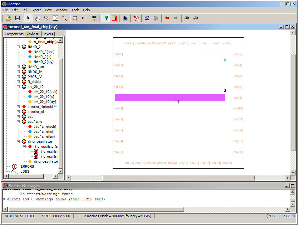
Next
make a layout view of A_final_chip
and place the NAND_2, inv_20_10, and ring_oscillator
layouts in the cell.
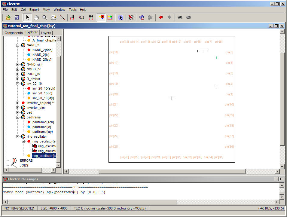
Let’s
next select the padframe
layout and set its properties so that it isn’t easy to select.
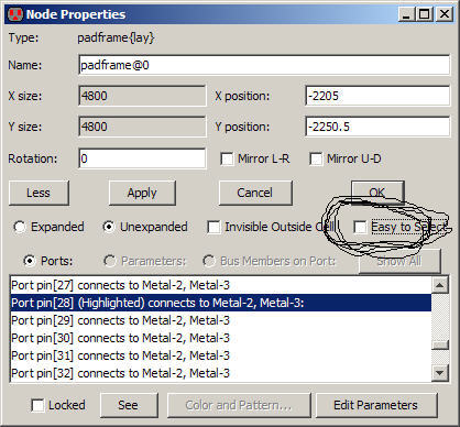
If
we don’t make the padframe
hard
to select then it will be difficult to select the other cells that are
occupying the same area.
Remember
this feature since it could lead to frustration (why
can’t I select this!!!)
The
issue is that we still need to be able to select parts of
the padframe (the
Exports labeled pin[1:40]).
This
is where the special select comes in handy (icon in the
middle of the menu).
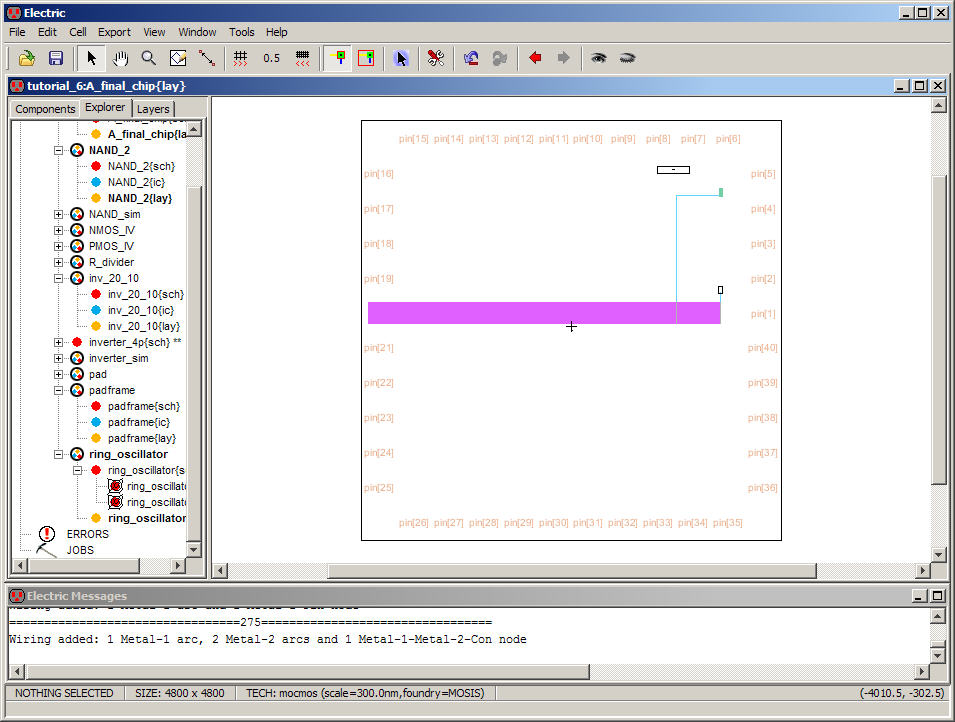
Use
the Toggle Special Select so we can select pin[20]
(ground).
After
selecting pin[20] Toggle Special Select again and then
right click on the ground connection of the NAND gate (zoom in so it’s
easier).
Below
is the result.
Connect
the ground up of the inverter next.
Note
that an important concern, that we aren’t covering here,
is the sizing of the conductors.
Here
we aren’t being practical but rather simply wiring the
chip up so that it matches the schematic.
Add
the other wire connections then DRC, NCC, and (after
Exporting gnd and vdd and
changing the text size to 125) Well Check.
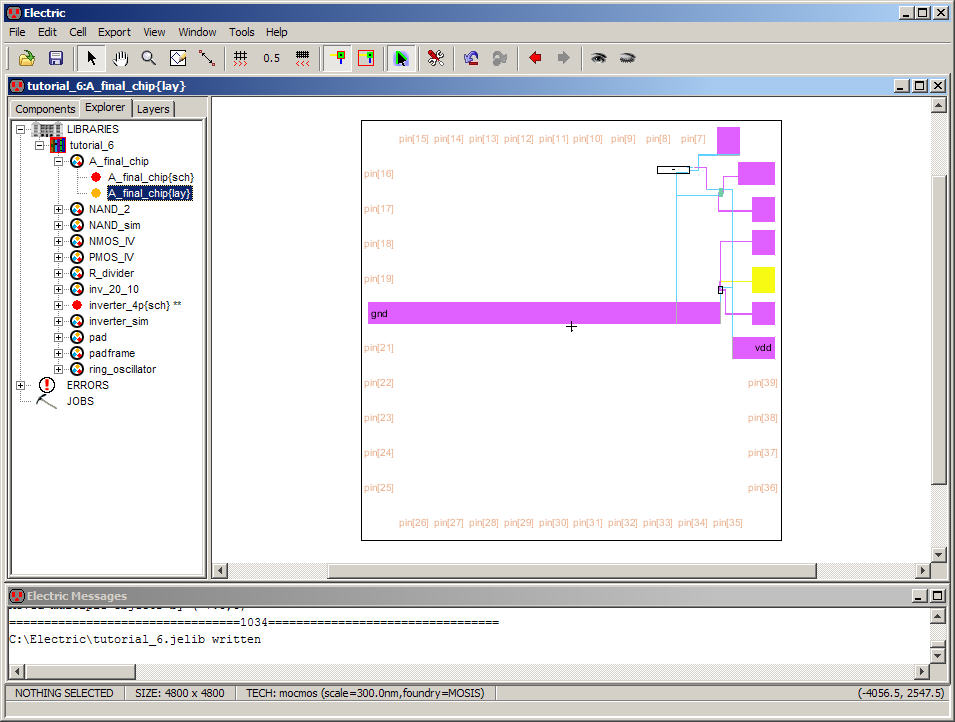
The
final layout (yours will likely look different) is seen
below.
The
GDS (stream) file for this chip can be generated using
the menu commands seen below.
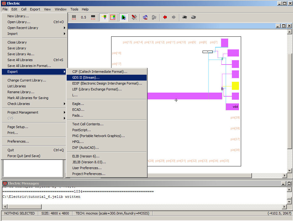
Once
we have GDS we can send it to MOSIS for fabrication
following the instructions seen here.
Save
the library.
This
is the end of the written Electric tutorials from CMOSedu.com
For
your reference the final jelib
used in this tutorial
is located in tutorial_6.jelib