Electric
VLSI Design
System
Tutorials
from CMOSedu.com (Return)
Tutorial
3 – Design, layout, and simulation of a CMOS inverter
In
this tutorial we’ll layout and simulate the operation of a CMOS
inverter using
the setups, and C5 process, from Tutorial 1.
To begin, use Electric to open the jelib we created in tutorial 2, tutorial_2.jelib (right click to save to C:\Electric).
Save
this library as tutorial_3.jelib, again in
C:\Electric.
Next
ensure that the C5_models.txt are
saved in C:\Electric for SPICE simulations.
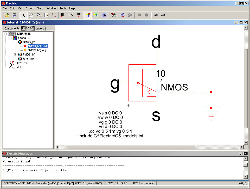
Next
open the cell NMOS_IV.
Select
the nMos Node and use Ctrl+C or Edit -> to copy
the Node to the clipboard.
Copying
the Node will eliminate the need for us to
re-position the W and L text and select a SPICE model.
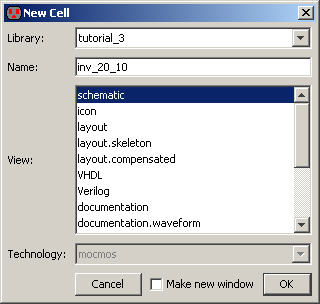
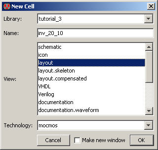
Next
create a new cell, Cell -> New Cell (or just use Ctrl+N) called inv_20_10 (an
inverter with a PMOS having a
width of 20 and an NMOS with a width of 10)
Ensure
the schematic view is selected.
Next
paste the nMos Node
copied
above into this new cell and then fill the window (zoom in around the
added
Node).
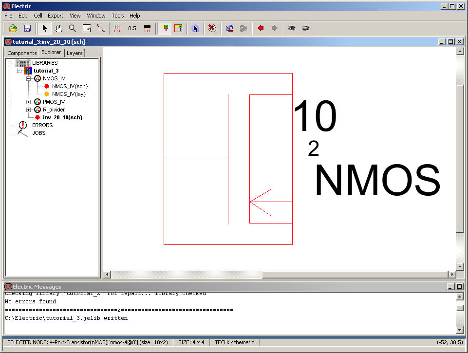
We
don’t need the symbol to show the body connection since
our NMOS body (the p-substrate or p-well) will always be at ground.
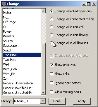
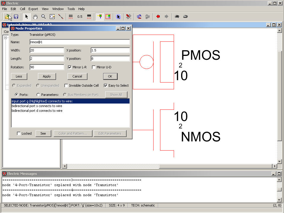
With
the nMos Node selected
go to
Edit -> Change (or simply press C) and change the Node to
transistor as seen
below.
Make
sure to hit Apply then Done.
Repeat
the above set of steps for the pMos
Node in the cell PMOS_IV to get the following.
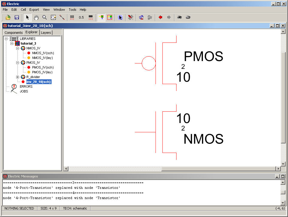
Since
want the PMOS’s width to be 20 change, by editing the pMos Node’s properties, 10 to 20
as seen below.
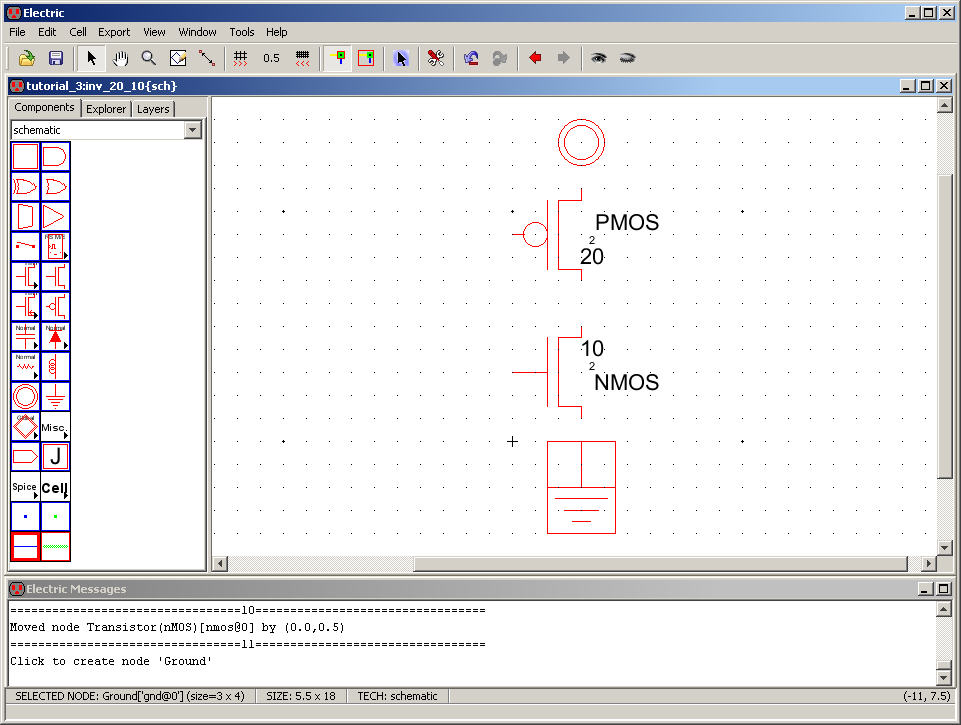
Next
turn the grid on and add the power symbol as seen below.
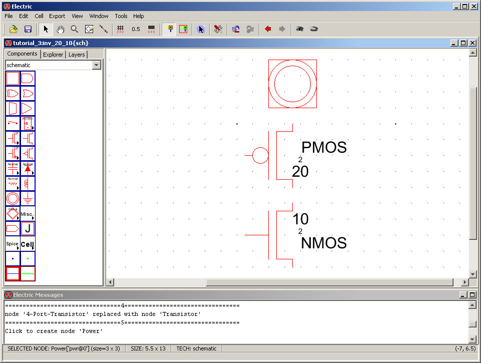
Next,
with the power Node active as seen above, use Edit
-> Size -> Interactively (or just Ctrl+B)
to
reduce the size of the power symbol, below.
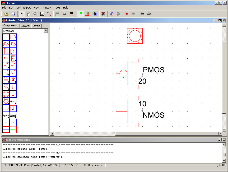
Align
the symbols to grid and add the gnd
Node as seen below.
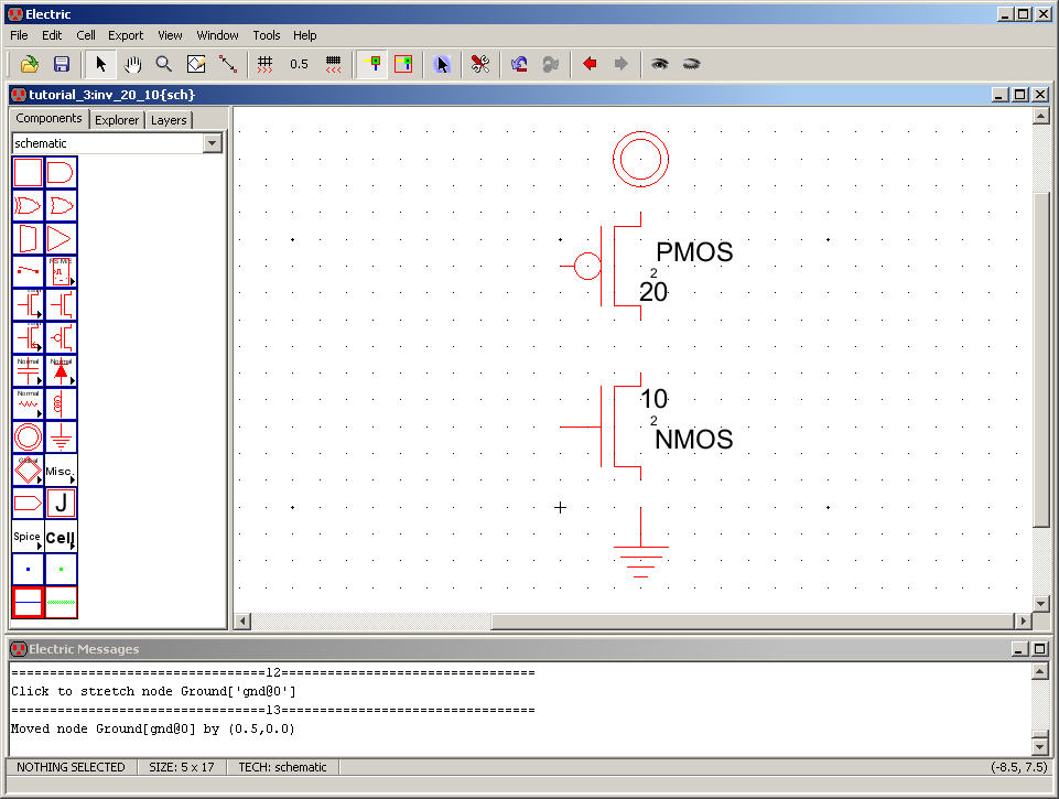
Go
ahead and reduce the size of the gnd
Node and move to align to grid as seen below.
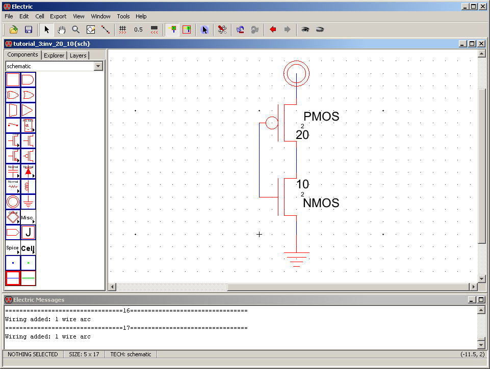
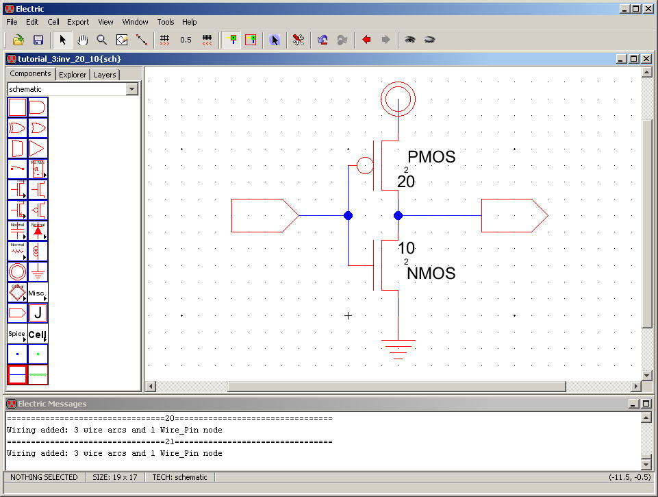
Add
the wire Arcs to wire the inverter together.
Remember
to use the left mouse button to select a port on a
Node and the RIGHT mouse button to make an Arc connection.
The
connection to the power Node is found in the center of
the Node.
Next
add Off-Page Nodes as seen below.
These
Nodes have ports on the left and right sides (it
doesn’t matter which one you connect to).
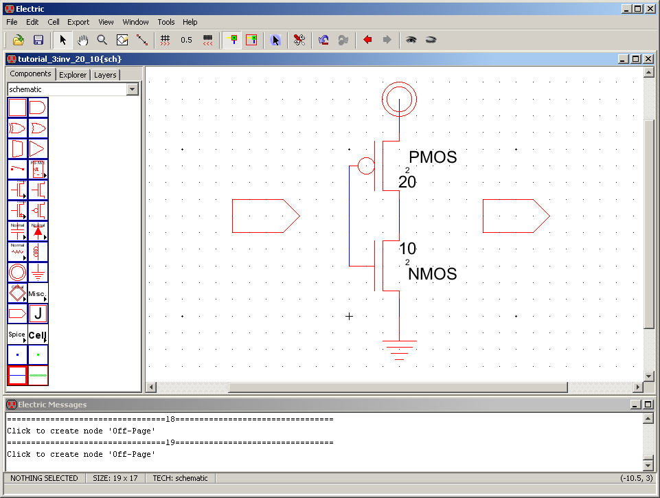
Connect
wire Arc’s to the Nodes as seen below.
Next
we want to Export the inverter’s input and output.
Use
Export -> Create Export (or Ctrl+E)
to export the input (select the left port on the input side as seen
below).
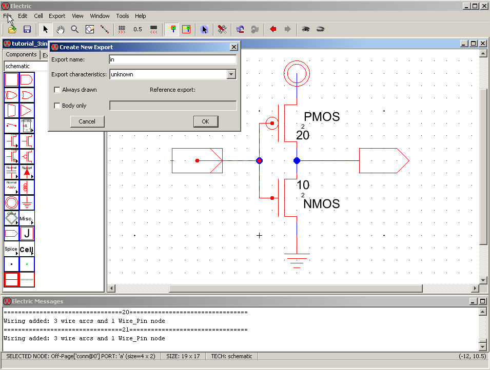
Repeat
for the output Off-Page Node (the right side port of
the right off-page Node).
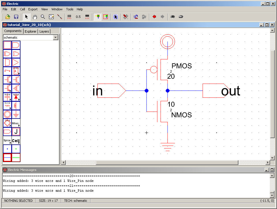
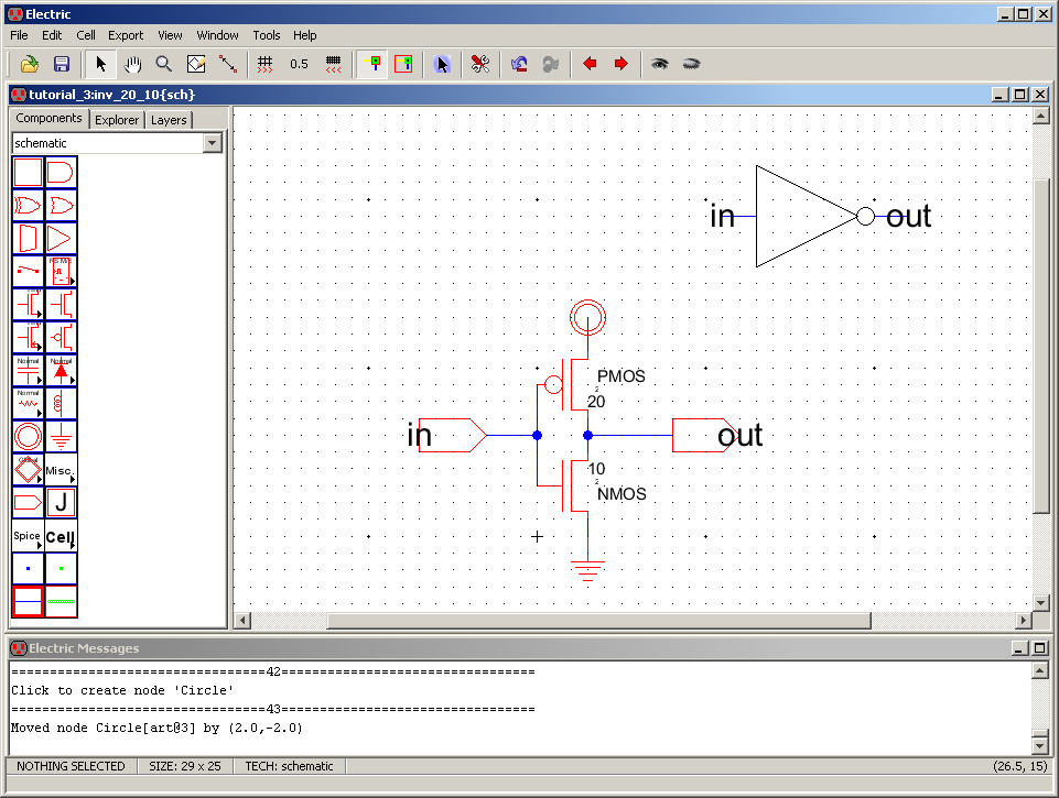
The
results are seen below. Hit F5 to check the schematic for
errors.
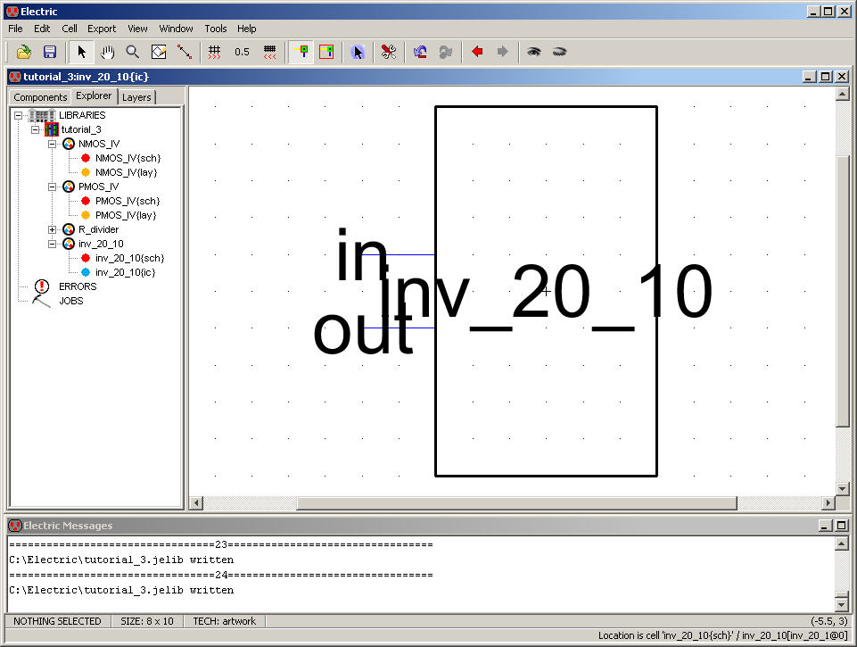
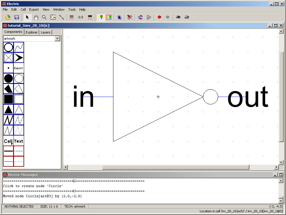
We
are now ready to create an icon view for this schematic.
Go
to the menu item View -> Make Icon View.
After
filling the window we get the following.
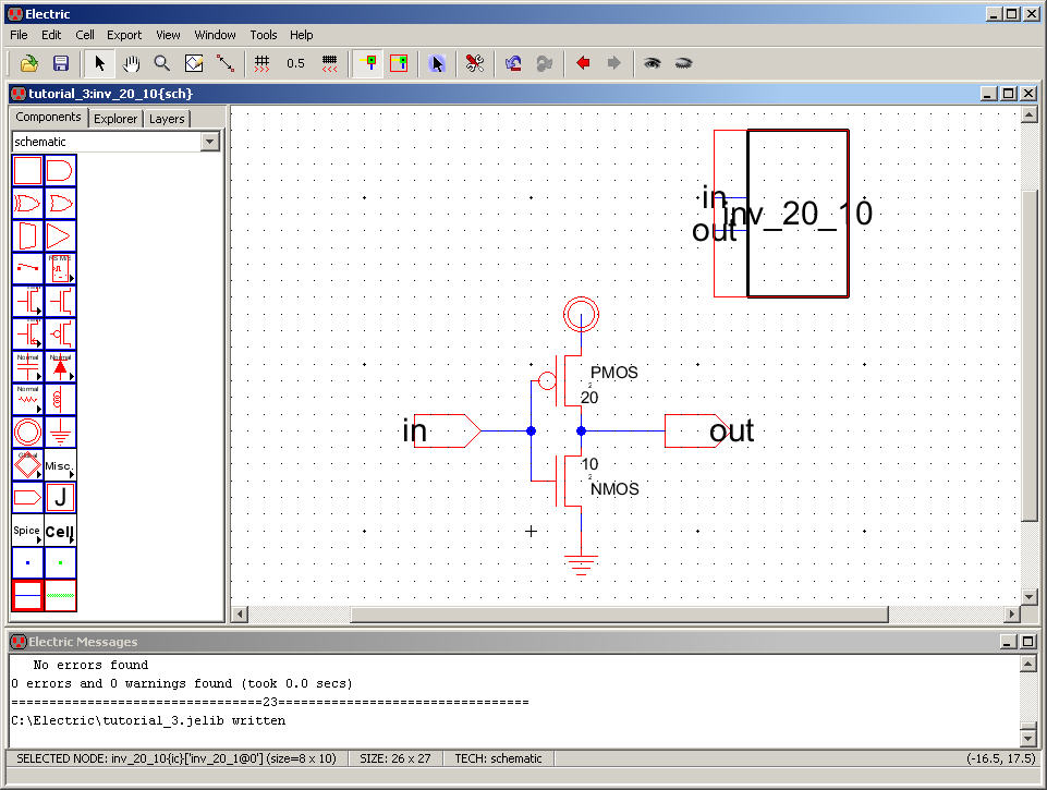
The
icon view was added to the top right hand side of the
cell.
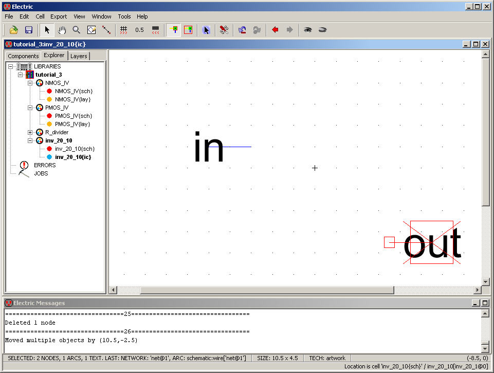
This
doesn’t look like an inverter so we’ll change it.
However,
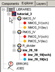
before doing so let’s click on the Explorer tab on
the left and expand the inv_20_10 cell group.
Notice
that blue indicates an icon while, again, red a
schematic and orange a layout view.
We
need to change the icon so that it looks like an inverter.
In
the schematic view an instance of the icon is placed.
We
can open the icon view by double clicking on the name
above or
by
selecting this view and going to the menu Cell -> Down
Hierarchy -> Down Hierarchy (or Ctrl+D)
Let’s
select the icon view in the drawing area and press Ctrl+D to get the following.
To
go back up in the hierarchy we can use Ctrl+U
or Cell -> Up Hierarchy -> Up Hierarchy
Press
Ctrl+U now to go back up
to
the inverter schematic (the only cell using the icon view)
Select
this view again and then Ctrl+D
to back into the icon view (knowing can use the Explorer to move
between cells
too)
Next
select and delete the box/text to get the following.
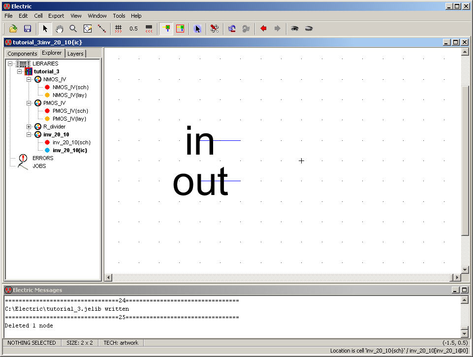
Select
the bottom set of items as seen below.
Rotate
these items (Ctrl+J is
the
fastest way) and move to get the following.
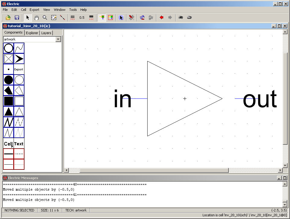
Next
go to the Component menu and select the triangle and
rotate to get the following.
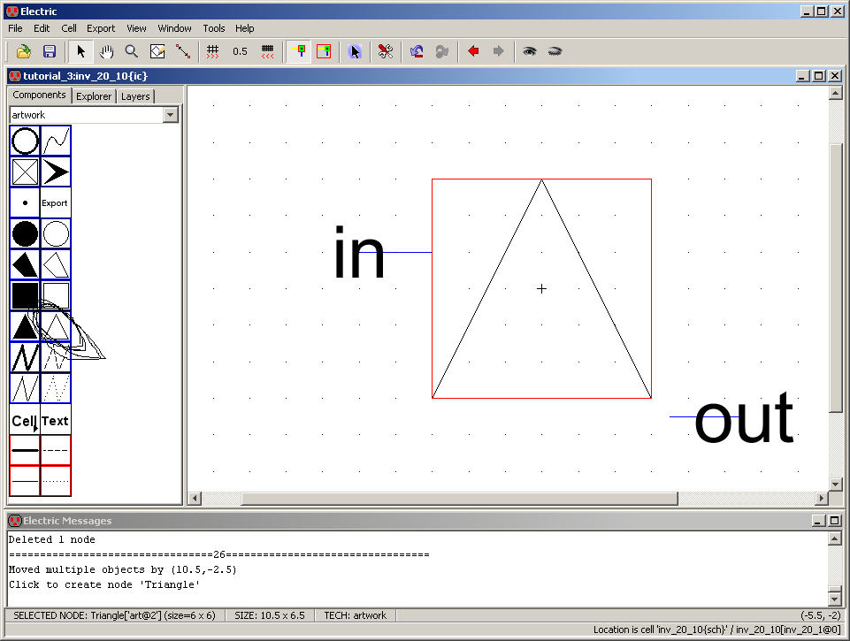
Rotate
the triangle and reposition the in/out items (Pin,
Arc, and Text) so you have the following.
Remember
the Shift+Click can be
used to select or de-select and item.
Next
select the circle and place it in the icon view.
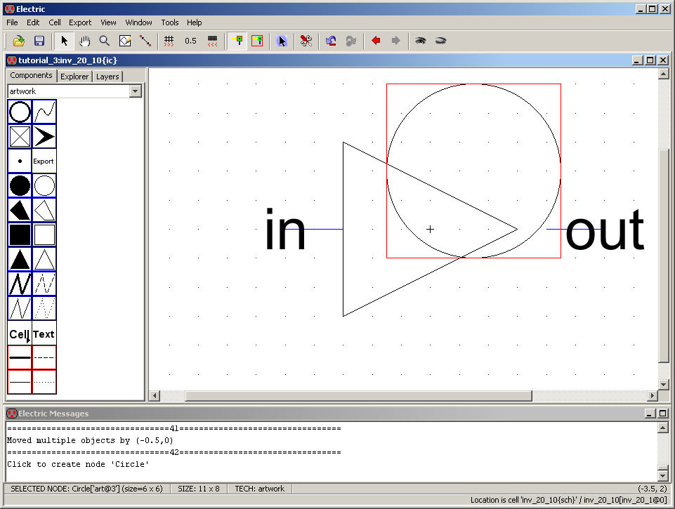
Edit
the properties of the circle (Ctrl+I)
to change x and y sizes to 1.
Reposition
the circle as seen below.
Our
icon view is now complete.
Press
Ctrl+U to go back up the
schematic view of the inverter (or use the Explorer).
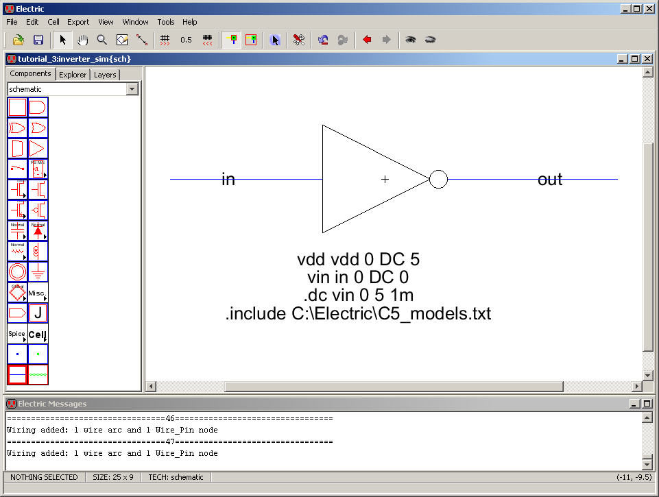
Let’s
simulate the operation of this inverter.
Create
a schematic call inverter_sim.

Next,
turn off the grid and then place the icon into this
schematic.
This
can be done in two ways.
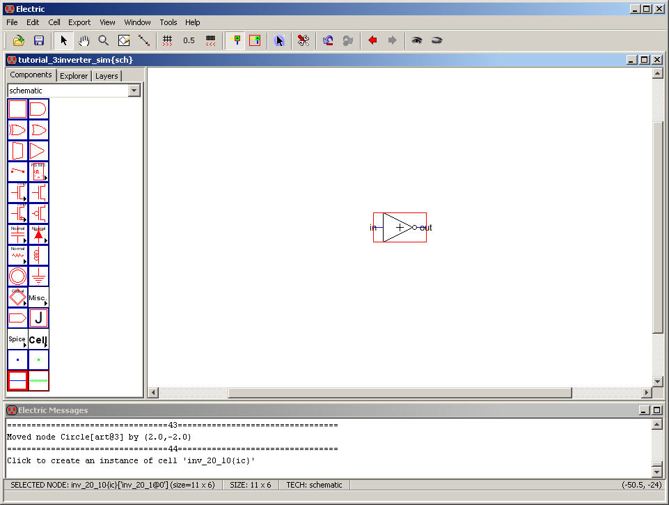
In
the Component menu select Cell -> inv_20_10 or
in
the Explorer click, and hold, on the cell you want to
instantiate and drag it into the drawing area.
Use
either method to place the inverter icon as seen below.
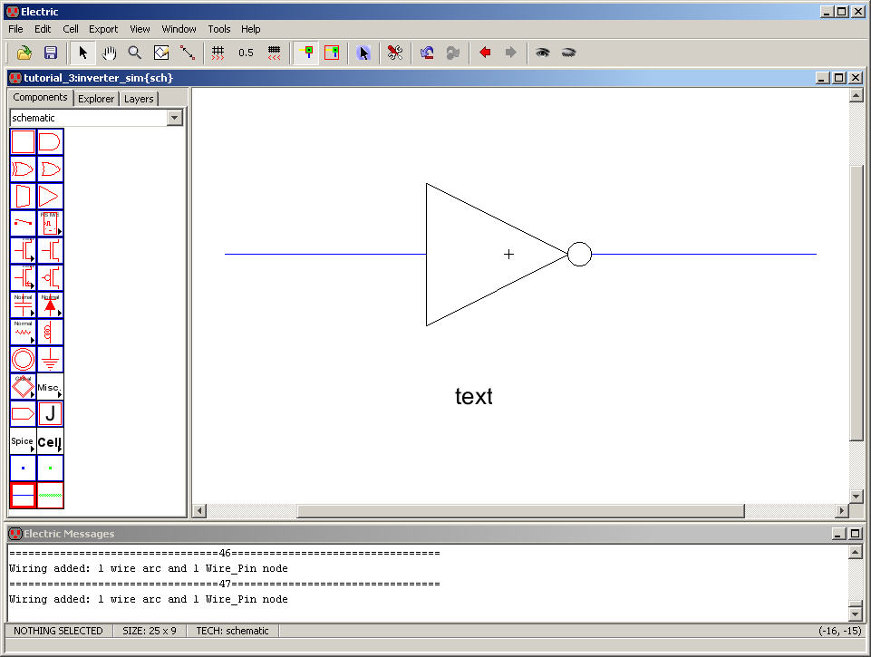
Add
wire Arcs to the inverter’s input and output.
Next,
add SPICE code (under the Misc. arrowhead) to get the
following.
Double
click on the Arcs (or select and use Ctrl+I)
to label the wires in and out as seen below.
Also,
edit the SPICE text so that the text seen below is used
(set to Multi-line text).
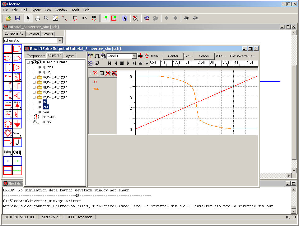
Using
the menu item Tools -> Simulation (Spice) ->
Write Spice Deck… gives the following LTspice output (after selecting
the in
and out voltages).
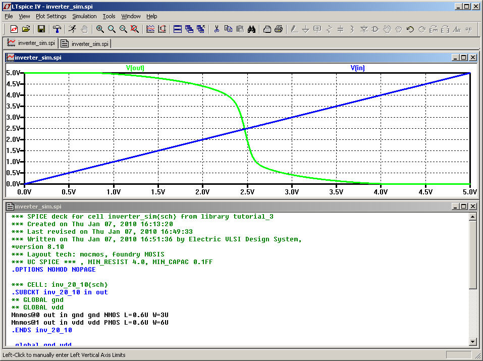
Closing
LTspice results in, again, after selecting the in and
out voltages:
Let’s
lay out the inverter next.
Create
a layout view for the inverter.
Now
there are three views in the inv_20_10 cell group:
schematic, icon, and layout
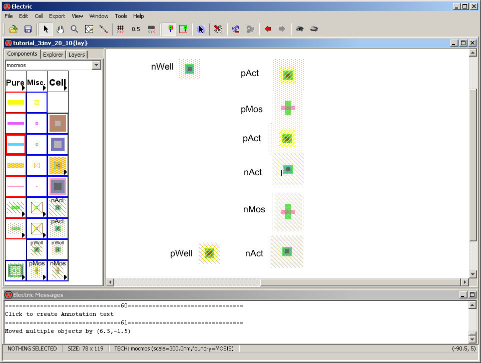
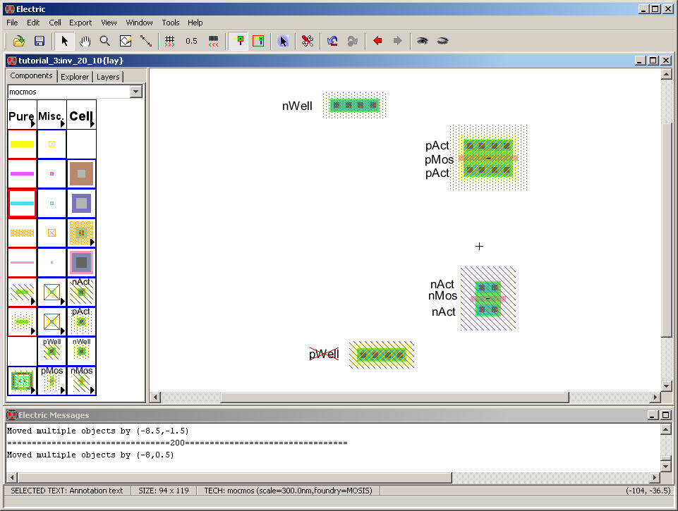
Add
the following Nodes to this cell.
Annotation
text was added to help know what to place and
where.
Next
select the pMos Node
and set
its SPICE model to PMOS (see Tutorial 2 if you don’t remember
how to do this) and set
the width to 20.
Next
select the nMos Node
and set
its SPICE model to NMOS and set its width to 10.
Keep
both MOSFETs lengths at 2.
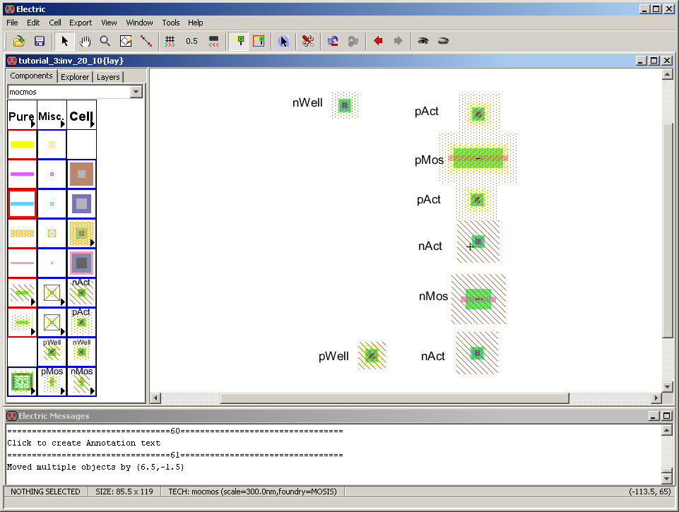
Next
set the x-size of both pAct
Nodes to 20 and both nAct
Nodes to 10.
Further
set pWell and nWell x-sizes to 20.
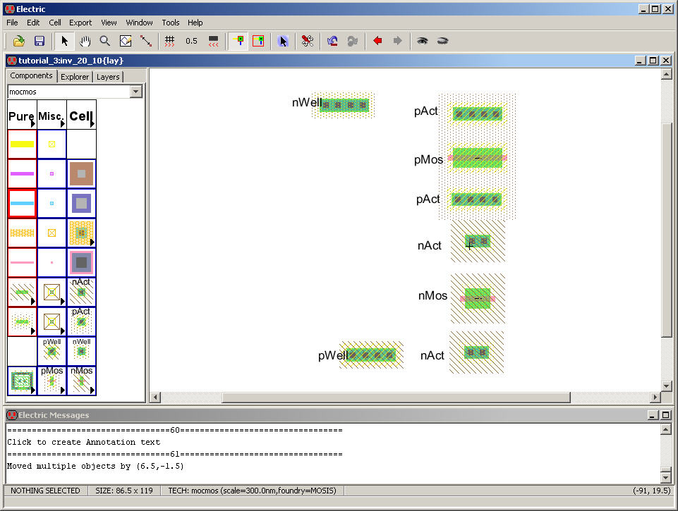
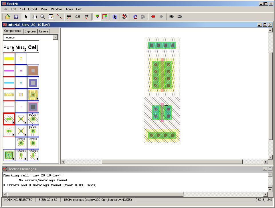
Next
add Arcs between transistors and active areas as seen
below.
Move
the active areas adjacent to the transistors.
Move
Annotation text for labeling too.
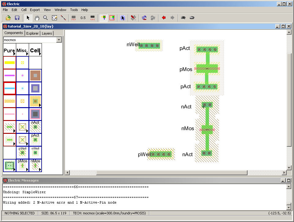
Let’s
delete the Annotation text.
Next
rotate the transistors and active areas and move the
devices into the positions seen below.
DRC
the layout to ensure no errors are present.
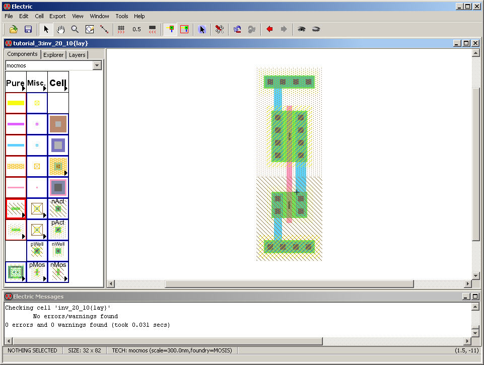
Next
connect: the two poly gates together, the metal on the
right of the devices together, and the metals on the left of the
transistors up
or down to the well connections as seen below.
DRC
your design.
Add
a poly1 to metal1 contact on the left and a metal1 Pin on
the right as seen below.
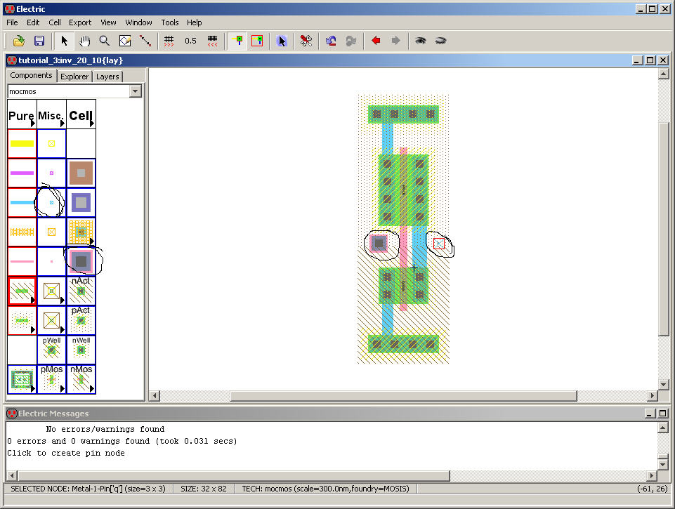
Connect
the Pin and Contact up as seen below.
If
the width of the poly1 isn’t 2 after the Arc is placed
simply select the Arc and change its width to 2.
DRC
the layout to ensure no errors.
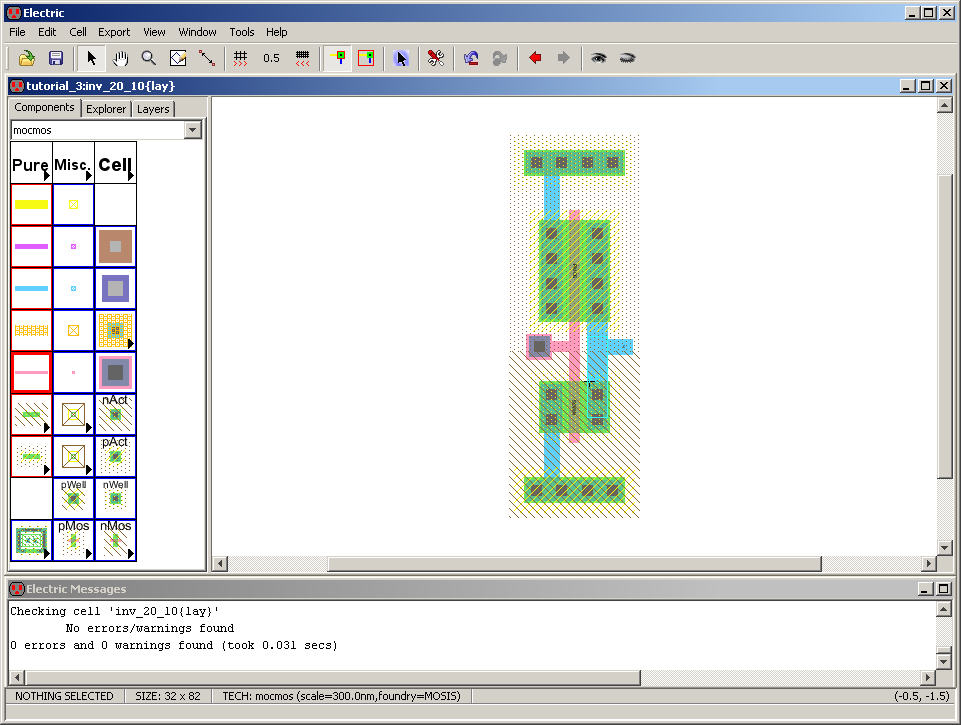
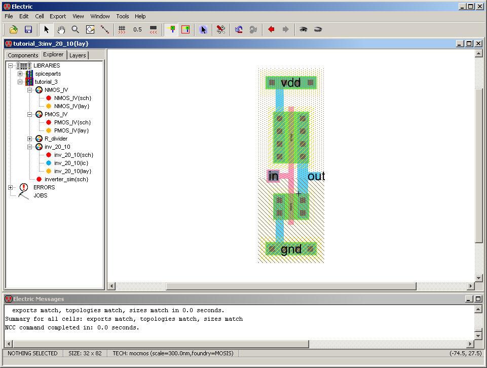
We
are now ready to Export in, out, gnd,
and vdd.
Select
the pWell Node and then
hit Ctrl+E as seen
below.
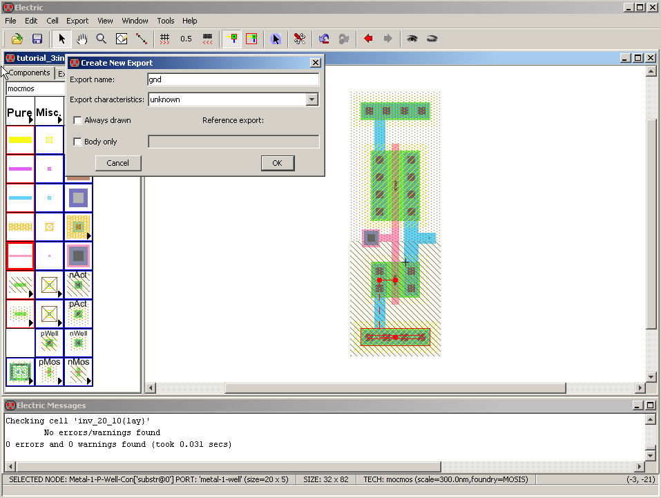
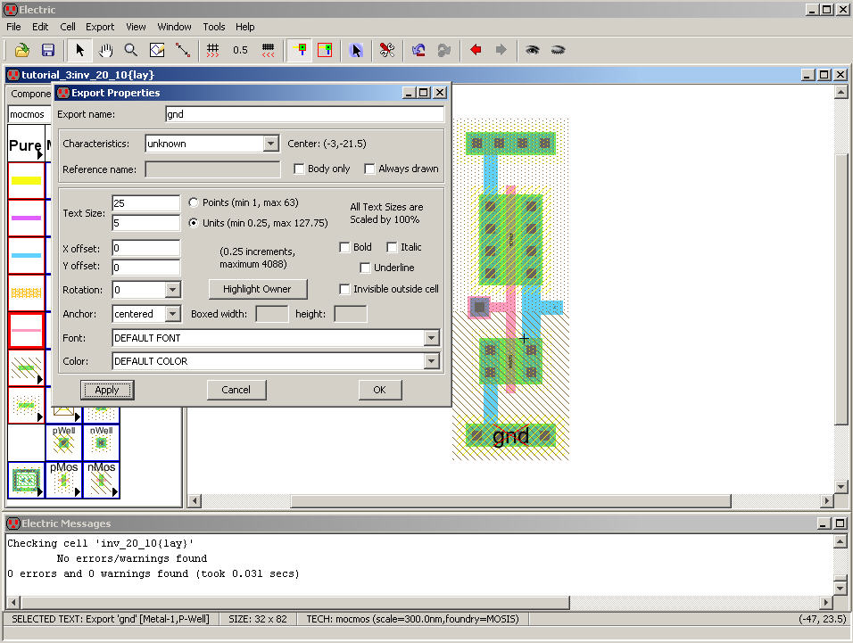
Select
this gnd Export and
change
its Text size to 5 as seen below.
Remember
that using the Crtl+click
is useful for cycling through the selections.
Also
remember that both gnd
and vdd exports must be
lowercase to properly NCC with the
corresponding power and ground schematic Nodes.
Next,
select the metal1 Pin we placed a moment ago (you can
only export Nodes, not Arcs, and the Pin is a Node).
Export
this Pin as out to match the schematic view.
Again,
change the size of the Text to 5 as seen below.
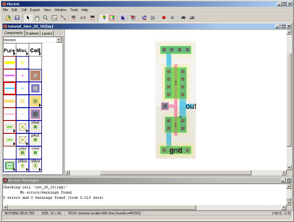
Repeat
for vdd and in then
DRC,
NCC, and Well Check the layout.
There
shouldn’t be any errors.
To
end this tutorial let’s simulate this layout.
Create
a cell named inverter_sim
with a layout view.
In
the Explorer Drag inv_20_10{lay} over into the drawing
area as seen below.
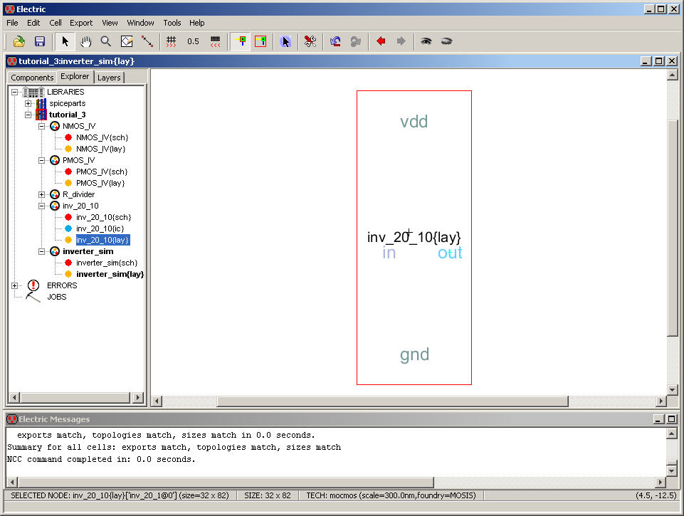
Notice
how we can’t see what’s inside the cell but we can see
the Exports.
With
the cell selected use the eye and closed eye on the
right side of the menu to toggle between showing and not showing the
contents
of the cell.
With
the cell selected edit the edit the cells properties (Ctrl+I), below.
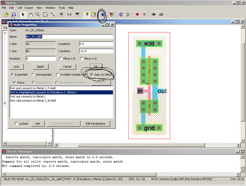
Notice
that you can de-select the “Easy to Select” feature
and make the cell hard to select. This is useful when the layout is
complicated.
If
a cell or layout is hard to select you can toggle the
“Special Select” cursor (circled on the menu).
Using
Pure layers, see menu item under the left Components
menu tab, requires the use of Special Select.
Let’s
connect metal wires to the cell as seen below.
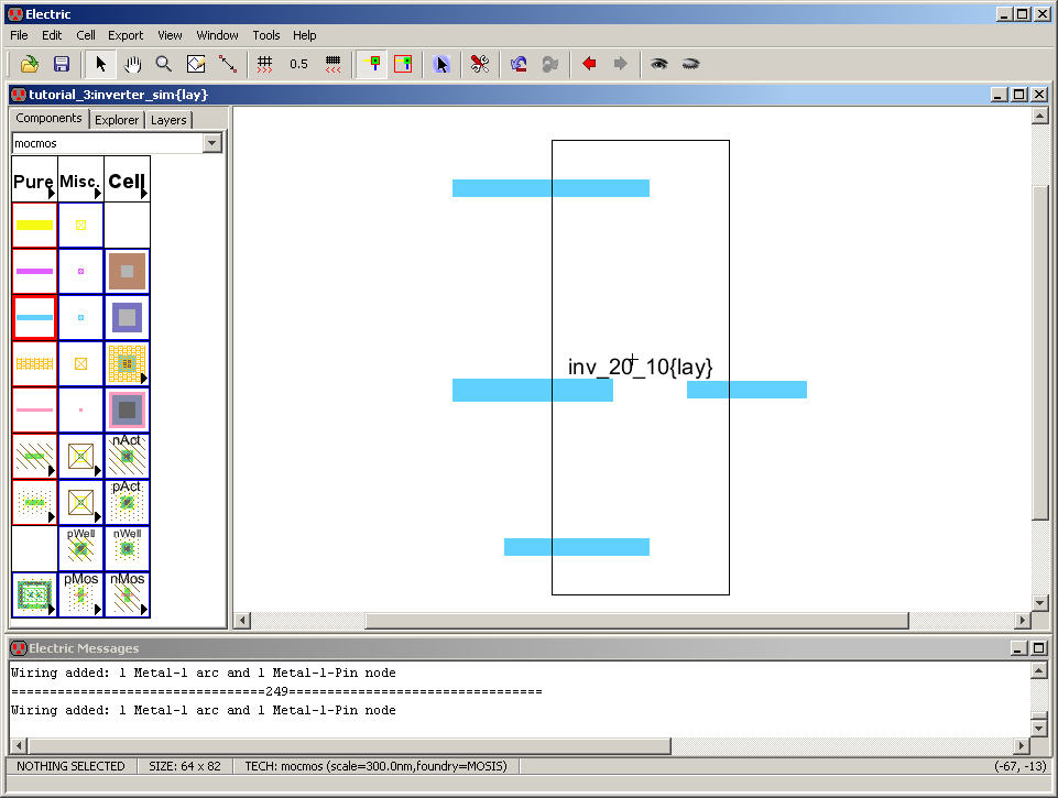
Next
edit the properties of the wire Arcs so that they
correspond to the names in the inverter_sim{sch}.
Next
copy the SPICE code from inverter_sim{sch} into this layout view of
the cell.
Change
the size of the SPICE code to 3 as seen below.
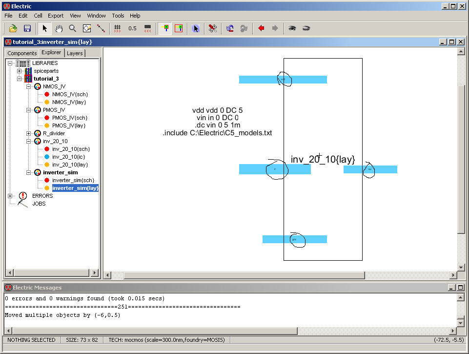
It’s
tough to see the wire Arc names so change their size to
5 (again Ctrl+click and
Shift+click
are always useful)
DRC,
NCC, and Well Check the cell inverter_sim.
We
get errors for both the NCC and the Well Checks.
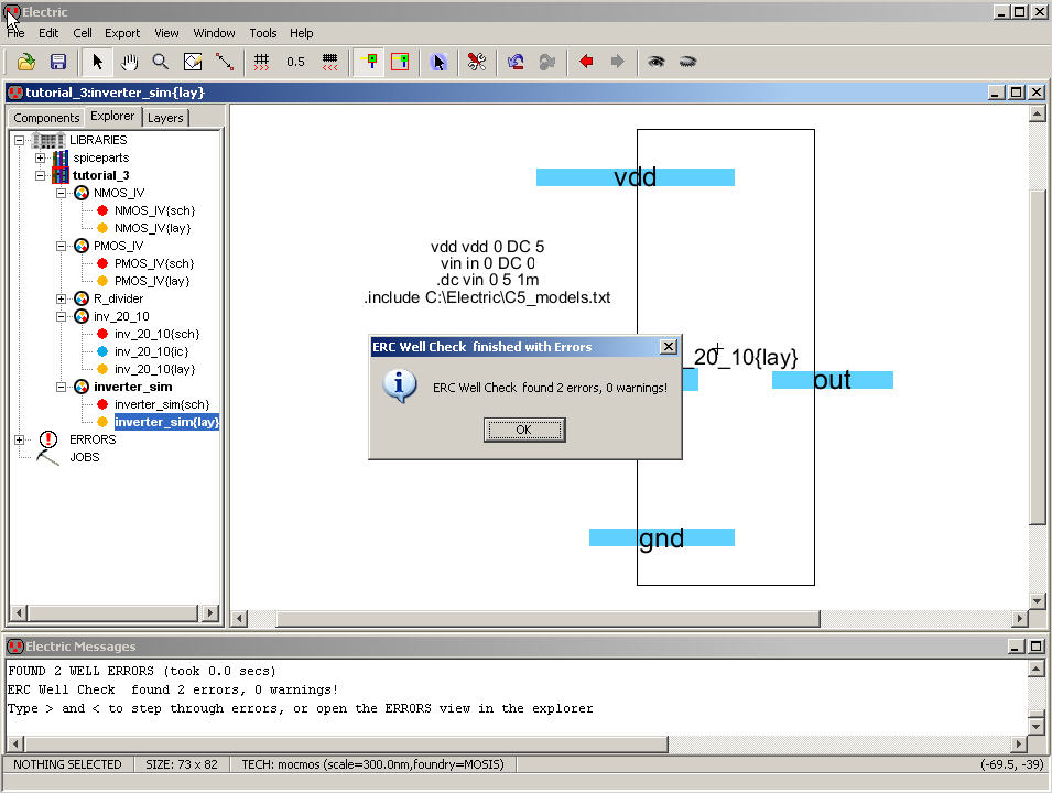
The
problem lies in the fact that since we used vdd
and gnd symbols in the
schematic we have to export them in the layout.
We
can’t simply name the Arcs vdd
and gnd like we did
above.
Delete
the vdd and gnd names from the Arcs.
Next
Export the left Pins on the top and bottom metal1 Arcs
with names vdd and gnd as
seen below (change text size to 5 too).
Again,
if you don’t use lowercase vdd
and gnd for the Exports
the layout and schematic
won’t NCC without errors (and the layout won’t Well Check correctly)
Notice
how the Exports could easily be mistaken for naming of
Arcs. It’s important to understand what we just did.
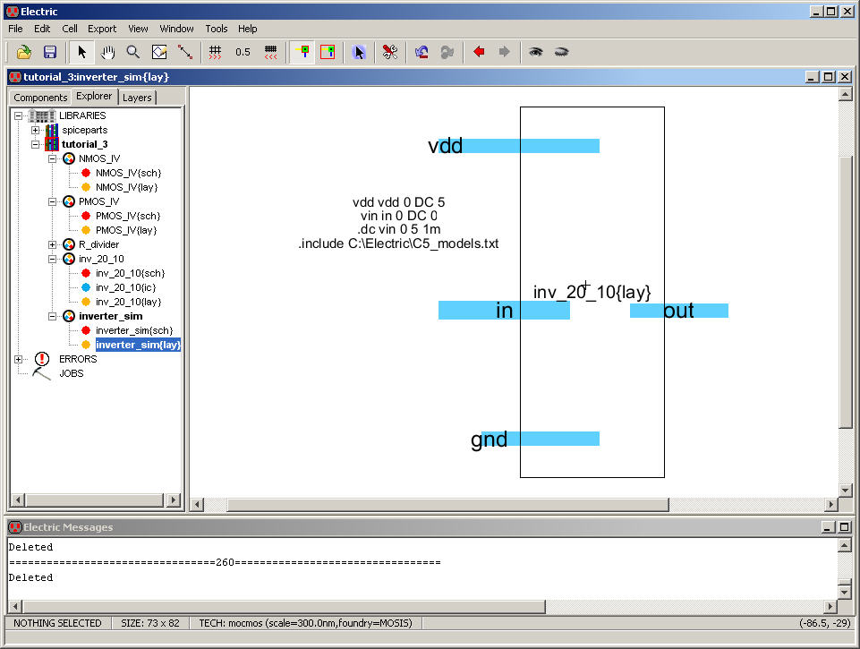
Now
the two cells DRC, NCC, and Well Check without errors.
Further,
the layout view of this cell can now be simulated
using SPICE (try this now).
This
is the end of the third tutorial.
For
your reference the final jelib
used in this tutorial
is located in tutorial_3.jelib