Cadence Design System Tutorials from CMOSedu.com
Cadence at CMOSedu.com
(examples, downloads, links, etc.) See items at the bottom of this page!
- Tutorial 1 – Layout and simulation of a resistive
voltage divider – cadence_tutorial_1_video.mp4 (57:50)
- Tutorial 2 – Layout and simulating the IV curves
of PMOS and NMOS devices – cadence_tutorial_2_video.mp4 (56:40)
- Tutorial 3 – Design, layout, and simulation of a
CMOS inverter – cadence_tutorial_3_video.mp4 (27:17)
- Tutorial 4 – Design, layout, and simulation of a
CMOS NAND gate – cadence_tutorial_4_video.mp4 (25:03)
- Tutorial
5 – Design, layout, and
simulation of a ring oscillator – cadence_tutorial_5_video.mp4 (25:23)
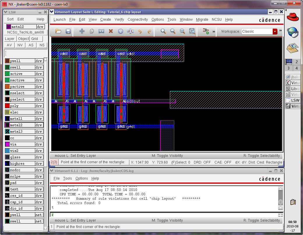
- Tutorial
6 – Placing circuit
layouts in a padframe for fabrication – cadence_tutorial_6_video.mp4 (71:47)
Below is some
other (random) material that may be useful.
- To check MOSFET sizes when you LVS see Tutorial 4 and search (Ctrl+F) for "size" or just go to the end of the tutorial
- Cadence
schematic aesthetics tutorial
- The use of inherent
connections
- Running a
parasitic extraction and simulating using Calibre PEX
- X Error of
failed request when trying to start Cadence IC51 in NX client
- Printing/Plotting
with Cadence
- Setting up
ON's C5 PDK and Calibre in Cadence IC51 is found here
- Copying a cell from one library to another is found here
- Helpful
hints for modifying .cdsinit are found here
- Layout
of a poly-poly capacitor in the C5 process using the NCSU Cadence Design
Kit (CDK) is found here
- Example
layout of a hi-res poly 10k resistor using the C5 process is found here
- Digital
pads with ESD protection (ground, vdd, input, and output pads) in the C5
process using the NCSU CDK are found here
- Analog
pads with ESD protection in the C5 process using the NCSU CDK are found here
- MIPS Senior Design Project - report, readme.zip, and CPU_TOP.zip
- Information on how to remove Cadence lock files is found at the bottom of the page here
- To
kill all of your processes, something you should do periodically when
exiting Cadence (to make Cadence run faster), enter the command kill -9 -1
Some recurring project issues (using the NSCU Cadence Design
Kit with the C5
[ami06] CMOS process):
- Using nmos/pmos schematic symbols (3 terminals) will not work with Diva LVS (see Tutorial 2).
- You must use the nmos4/pmos4 symbols in schematics to LVS!
- For each cell there should be a schematic view, a symbol view, and a layout view (important, if a cell doesn't have a layout view you aren't doing it right).
- Drafting
the top-level schematic consists of drawing wires between symbol views
- Drafting
the top-level layout consists of connecting metal between the layout
views
- Using the calculator, an example: 1) select signal, 2) open calculator, 3) select function (e.g., average or rms, if you select the integrate function then you'll need to enter the limits of the integration) and then select OK at the bottom, and 4) press the calculate icon (see numbers on image)
- Efficiency of a power supply (powered with an input voltage VDD), E, can be calculated using E = (power supplied to the load)/(power supplied to the power supply) = (Vout * Iload)/(VDD * AVG(I(VDD))) where AVG(I(VDD)) is the average (see page 4 here) current pulled from VDD by the power supply.
- A parametric sweep (e.g. temperature), in a transient simulation, is done by: 1) selecting Tools in the ADE, 2) setting the Variable to "temp" and 3) setting the range (example, where 5 simulations are run at 0, 25, 50, 75, and 100)
- Convergence
of a simulation, expecially one using feedback as used in a switching
power supply, can be improved by allowing the power supply, vdd, to
ramp up to it's final value using a vpulse for vdd instead of vdc.
One may set the pulse delay to 0, the rise time to 10us, the initial
voltage to 0 and the final pulse voltage to 5 (then vdd = 5 after it
rises from 0 to 5 in 10us)
- If you can't add an output to plot in the ADE, select a component in a schematic, etc. then you might have accidentally changed the mouse so it only selects, for example, wires
- When running an LVS select Form Contents to ensure the tool points to the correct library. Of course you can copy the divaLVS.rul, divaDRC.rul, and divaEXT.rul files from ~/ncsu-cdk-1.6.0.beta/lib/NCSU_TechLib_ami06/ to the directory or directories you are working in to avoid path issues
- In the wavform viewer putting your cursor on a trace and pressing "a" then putting your cursor over another trace or part of the waveform and pressing "b" will indicate the time-difference between the two points
Return to:
