Cadence
Design System
Tutorials
from CMOSedu.com (Return)
Tutorial
2 – Layout and simulating the IV curves
of PMOS and NMOS devices
In
this tutorial we’ll lay out and simulate the operation of
NMOS and PMOS transistors using the C5 process from Tutorial
1.
Note
that we’ll simulate both the schematic and layout
(extracted) views.
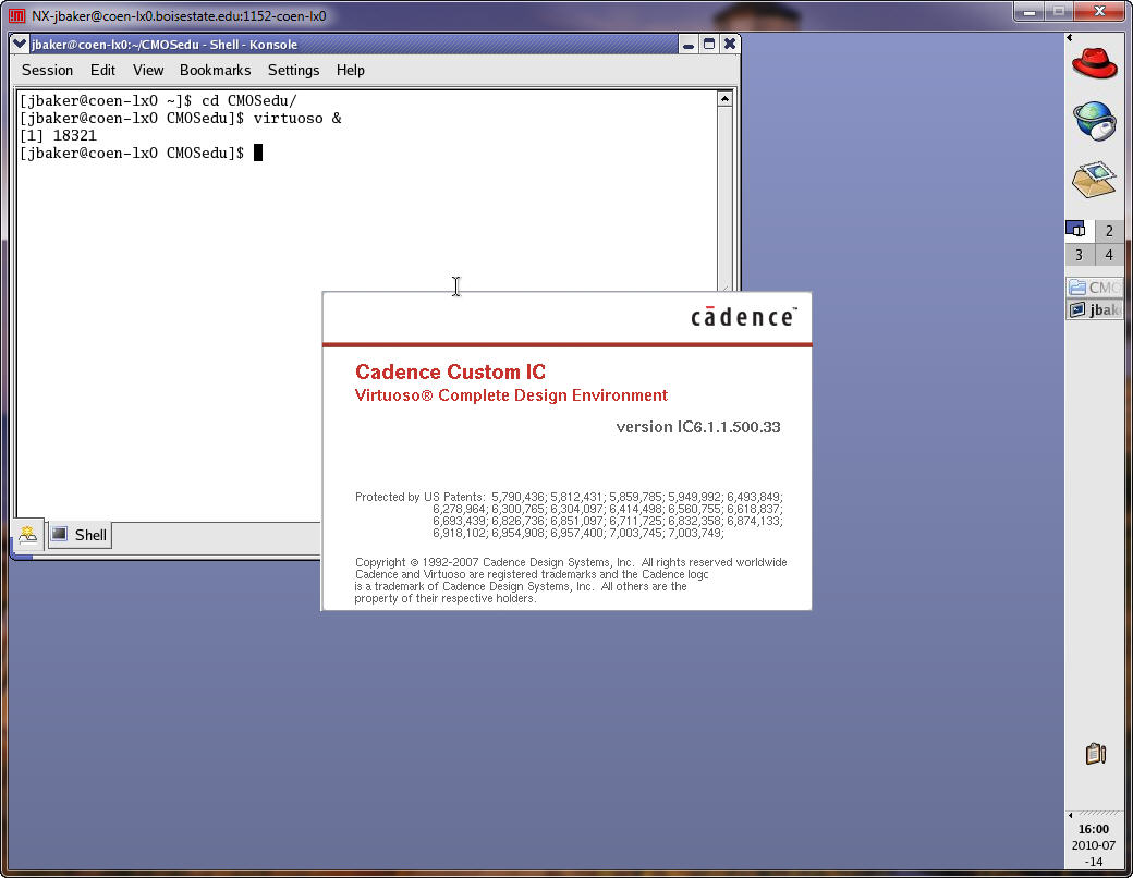
To
begin Tutorial 2 first start Cadence’s Virtuoso in the
CMOSedu directory as seen below.
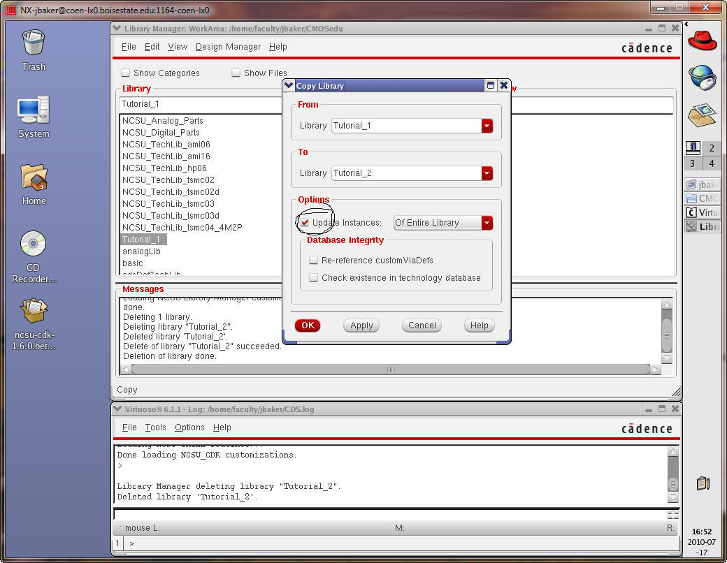
Next
copy Tutorial_1 into a new library called Tutorial_2 by
right clicking on Tutorial_1 (below).
Note
that if you don’t select Update Instances many of the
cells in Tutorial_2 will reference Tutorial_1 (we want the libraries to
be
self-contained).
After
pressing OK you will be asked where the Tutorial_2
directory should be placed. The default location should be the same as
Tutorial_1,
that is,
CMOSedu,
so hit OK a second time to create the library.
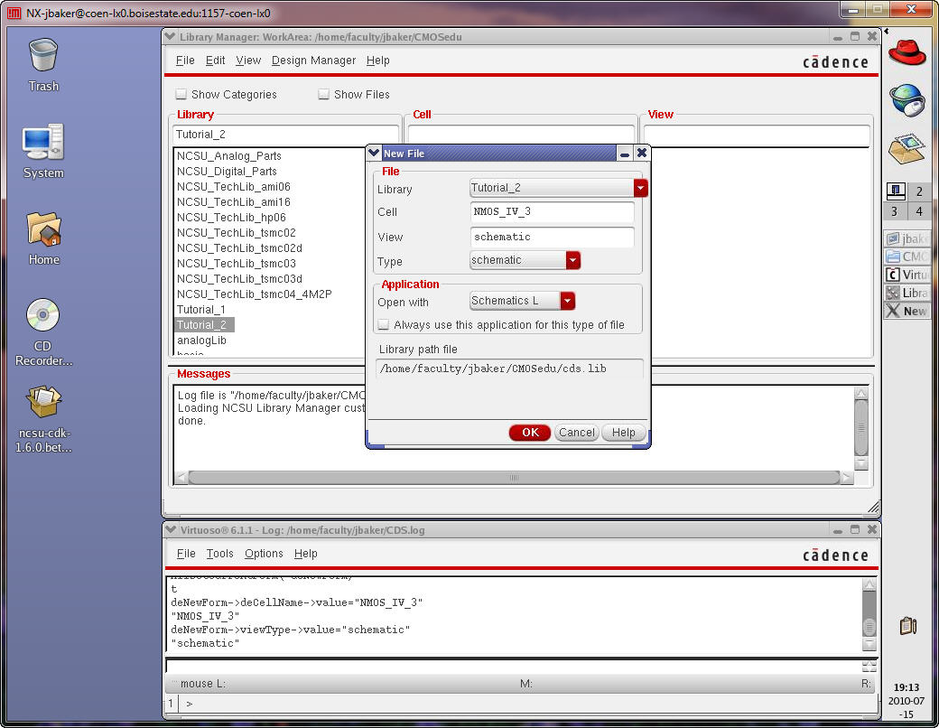
Next,
with the Tutorial_2 Library highlighted, select in the
Library Manager File -> New -> Cell View.
Create
a schematic cell called NMOS_IV_3 as seen below. The 3
indicates we’ll use a 3 terminal transistor.
Using
a 3-terminal NMOS the body (p-well or p-substrate) is
connected to gnd!
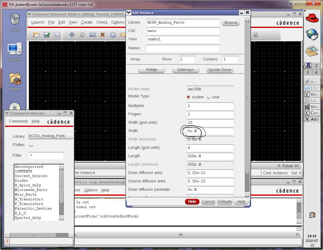
Press
i
(or use the menu Create -> Instance) and select, in the
Component Browser
Window, NCSU_Analog_Parts,
N_Transistors,
nmos.
Remember
that often Windows are opened that are behind other
windows so you have to use the Task bar to bring them to the front.
Set
the transistors Width to 6u and leave its length at 600
nm.
Place
the transistor and fit the screen (press f).
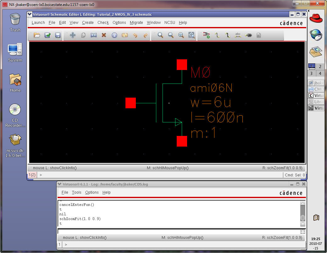
Next
add Pins with the direction inputOutput
and wires as seen below.
Remember
that right+clicking the
mouse when instantiating the Pin rotates it.
Z
(zoom out by 2) and f (fit) can be
used while instantiating
the pin.
w
can be used to wire the
Pin to the MOSFET.
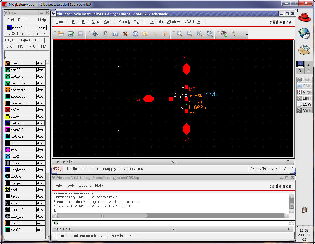
Check
and Save the schematic when finished.
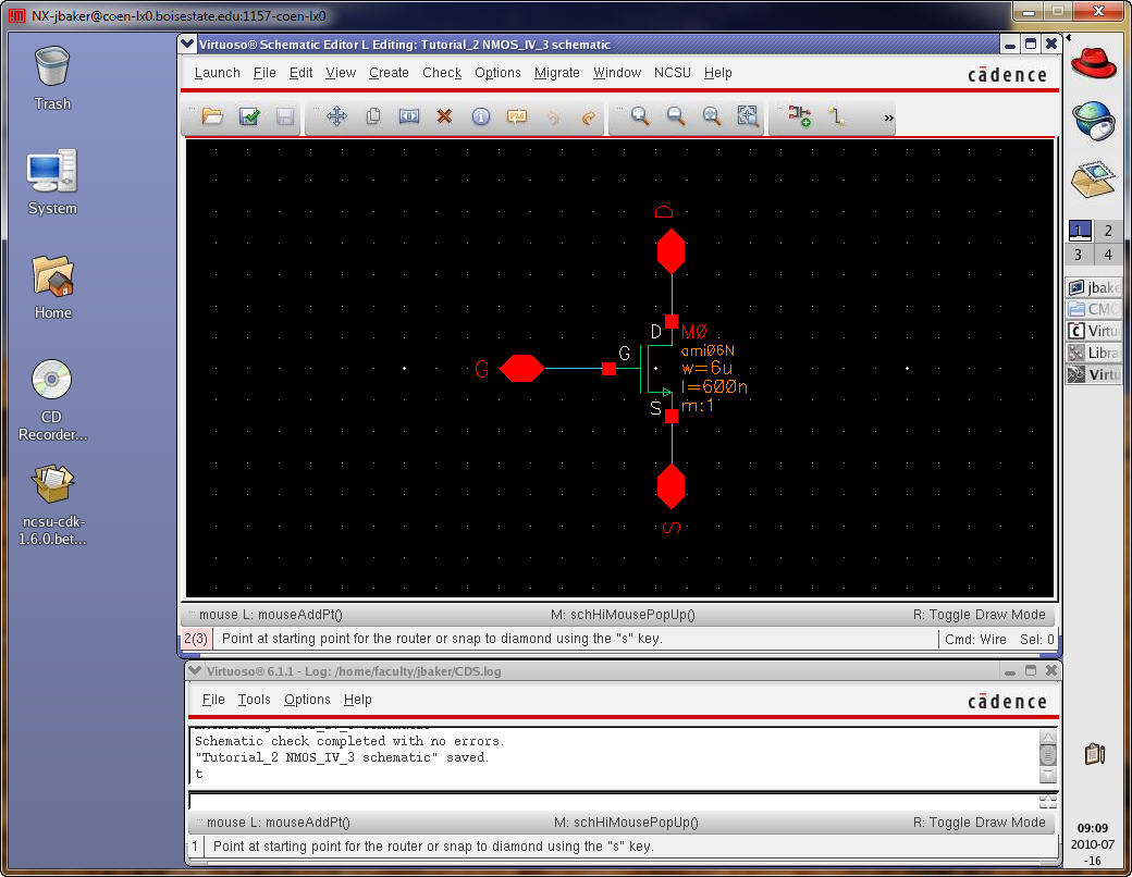
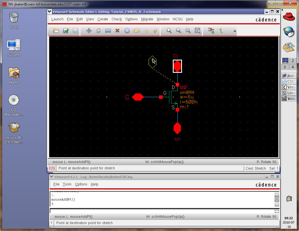
Before
making a symbol for this schematic let’s talk about
stretching (Bindkey s).
We
know that to move an object we select it then press m.
Stretching
is similar except that the object stays attached
to the wire or whatever you haven’t selected.
Below
is an example.
Next
create a symbol view for this schematic.
Create
-> Cell View -> From Cell View
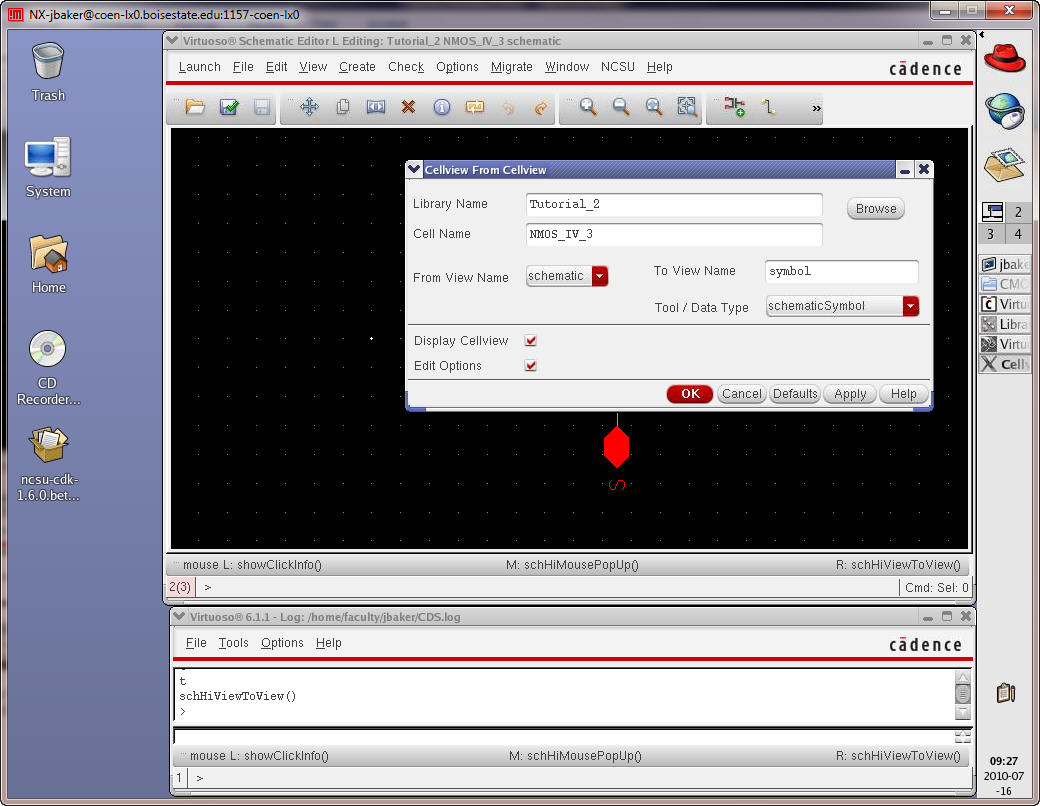
Virtuoso
will ask where the pins should be located (it
doesn’t matter). Hit OK.
Delete
everything in the cell except the pins.
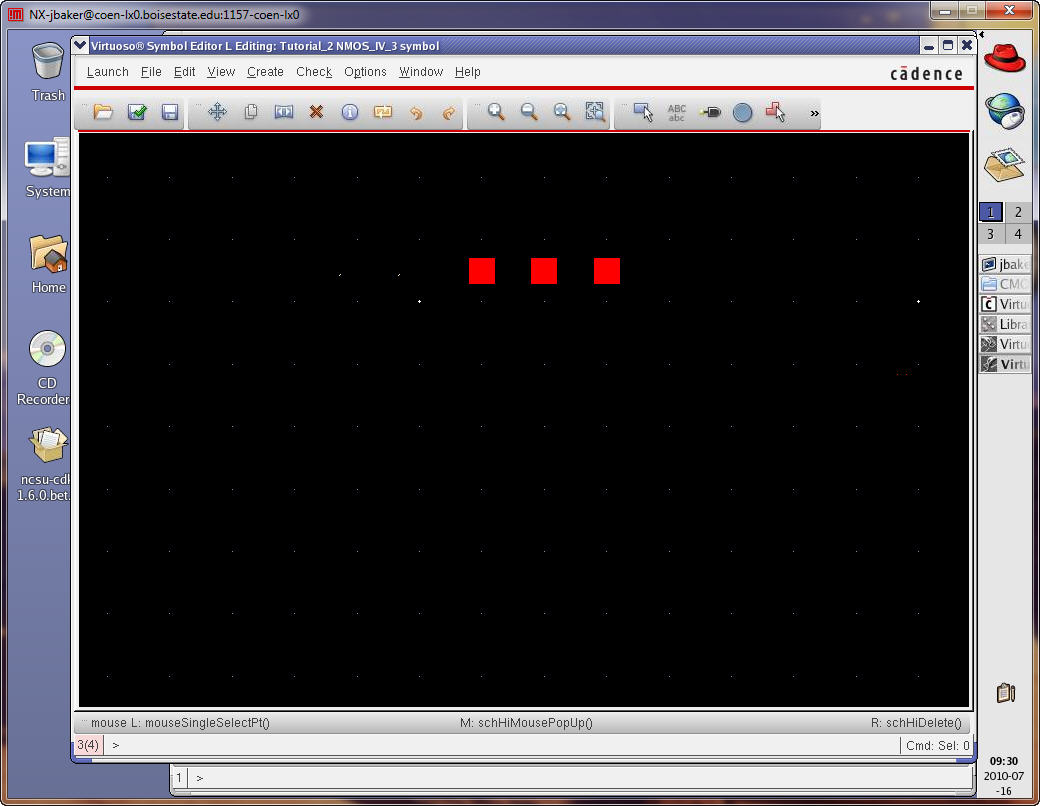
Notice
we can’t see the pin names.
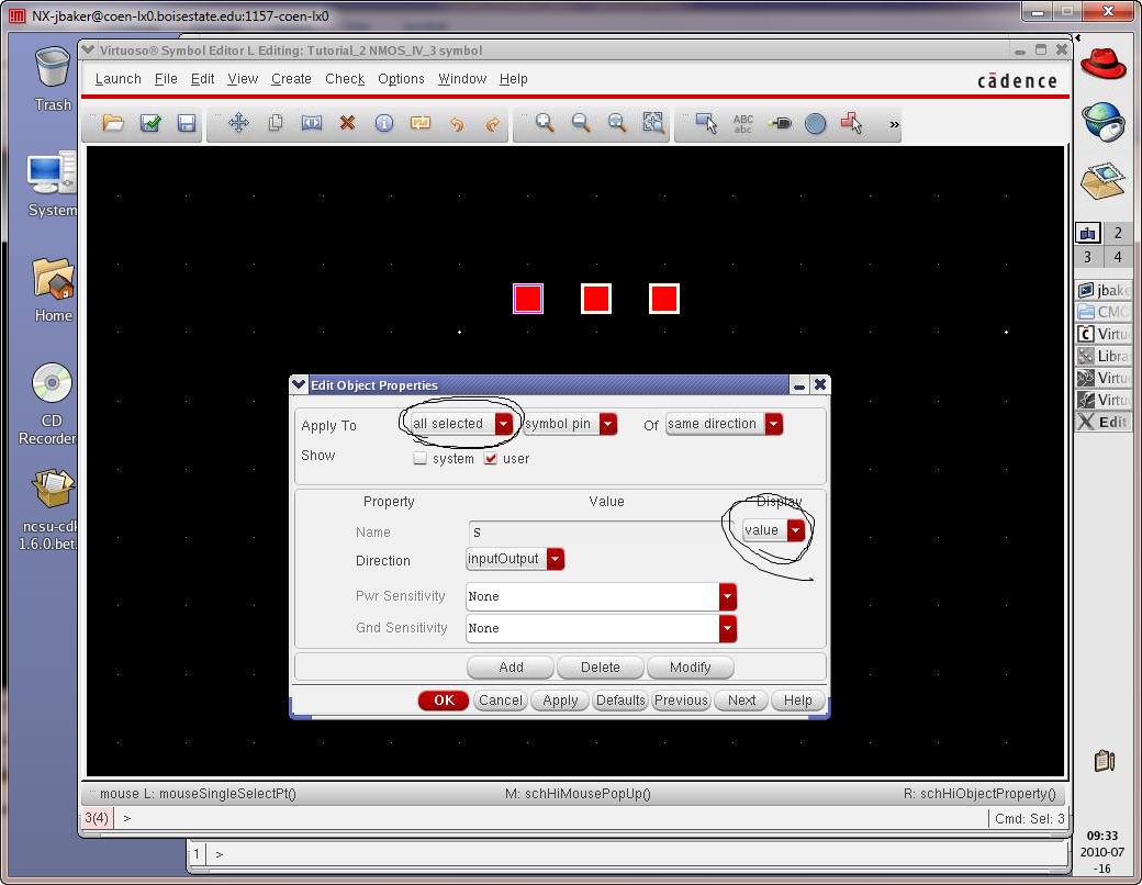
Select
all of the pins and then edit their properties (q).
Select
“all selected” and Display “value” as seen below.
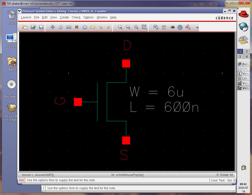
Draw
a MOSFET symbol and move the pins (rotate as necessary)
to get (something similar to) the following.
Remember
to draw a line use Create -> Shape -> Line.
Adding
the width and length text using Create -> Note
-> Text
When
finished “Check and Save”
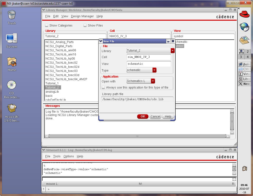
Next,
create, File -> New -> Cell View, a cell
(schematic) called sim_NMOS_IV_3.
Instantiate
the NMOS_IV_Cell View
just created and the DC voltage sources seen below (and wire things
together).
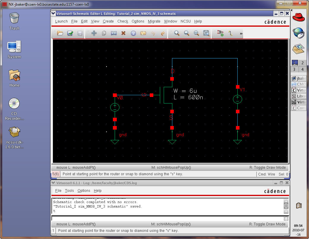
Notice
how the wires are drawn through the pin names? This is
sloppy so let’s fix it.
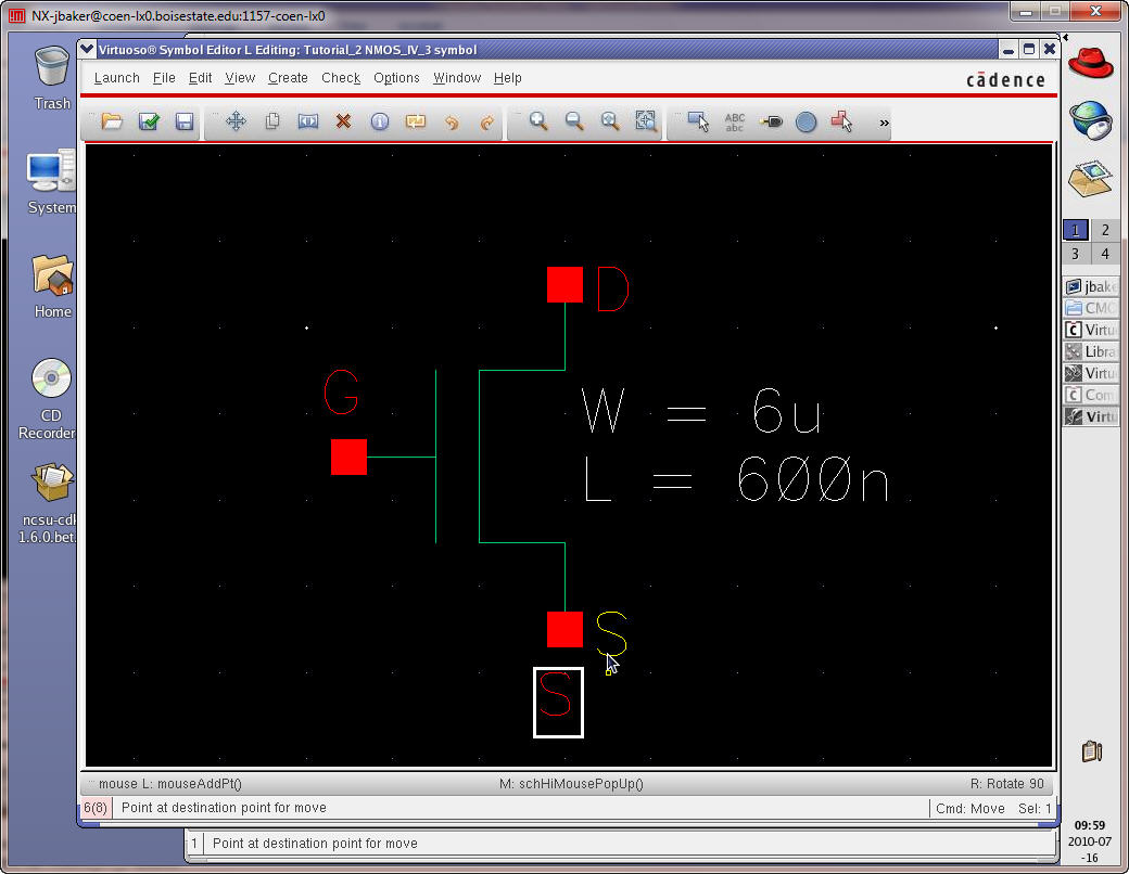
Use
the Library Manager to open the NMOS_IV_3 symbol.
Move
the labels as seen below. You’ll need to rotate the G
once and the S twice (right+click
the mouse while
moving).
“Check
and Save” the Symbol, close it, then return to the
sim_NMOS_IV_3 schematic.
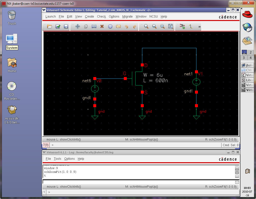
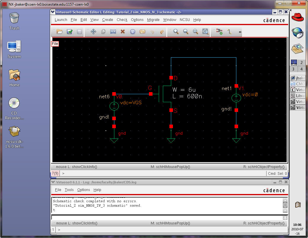
We
are almost ready to simulate.
Set
the value of V0 to VGS and the value of V1 to 0 as seen
below.
Check
and Save the schematic.
Launch
the ADE.
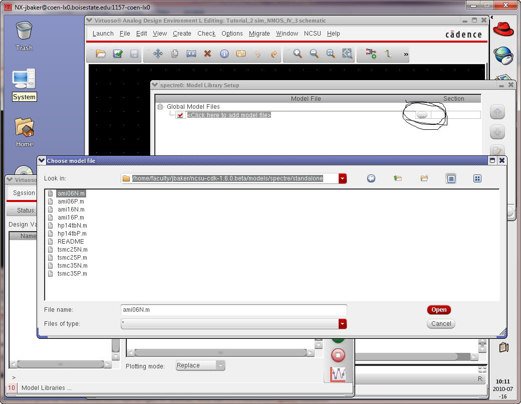
Go
to the menu Setup -> Model Libraries press the button
circled below and navigate to /$HOME /ncsu-cdk-1.6.0.beta/models/spectre/standalone
Select
ami06N.m (NMOS model) then Press Open and OK.
Note
that for general purpose simulation we would also select
ami06P.m for the PMOS models.
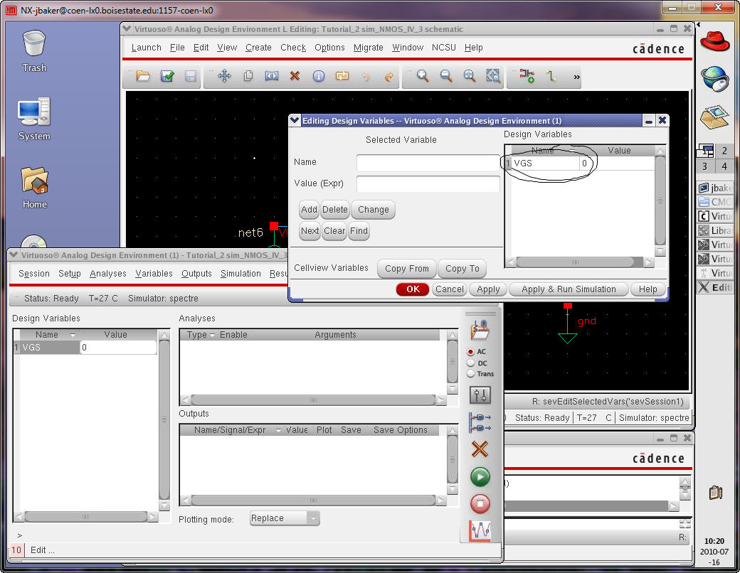
Next,
in the ADE window, select Variables -> Edit and add
VGS (value for the left DC voltage source in our schematic) and an
arbitrary
value of 0.
Press
OK and notice how the Design Variable shows up in the
ADE.
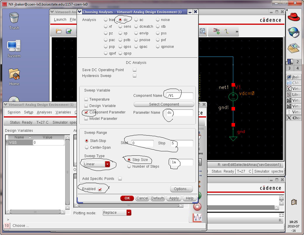
Next
select Analyses -> Choose and set the parameters seen
below.
Note
that V1 is the right DC voltage source in the schematic
connected to the Drain.
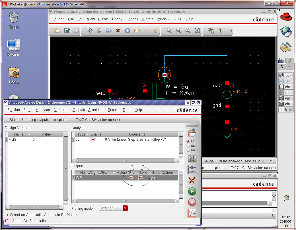
Select
Output -> To Be Plotted -> Select On Schematic
and click on the D Pin to select the current.
Ensure
that both plotted and saved are selected, circled
below.
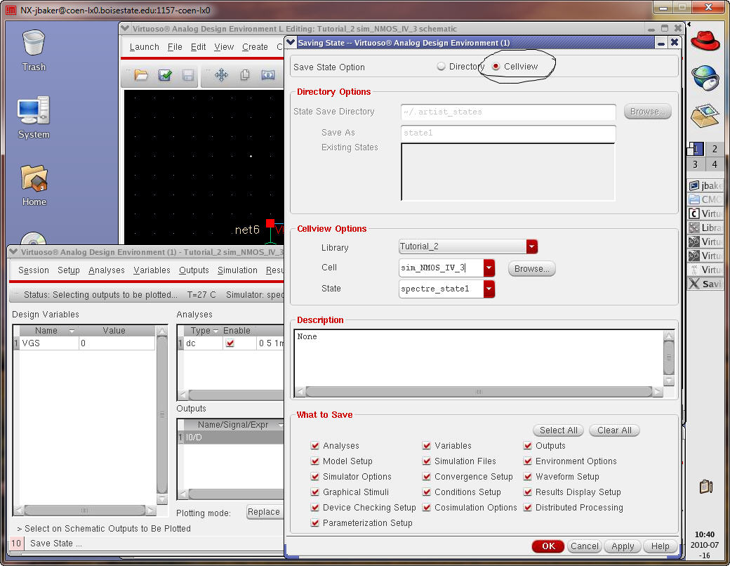
Now
let’s save the simulation state.
Select
Session -> State and save the in the Cell View (you
can use the Library Manager to verify it has been saved).
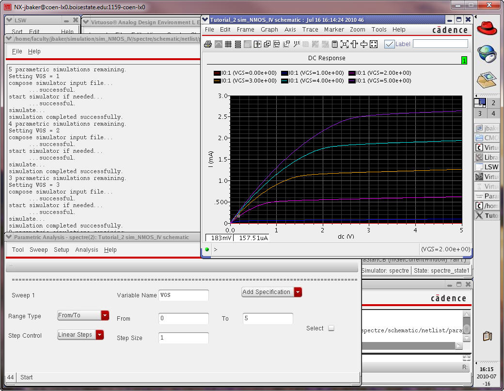
Next
choose Tools -> Parametric Analysis and set the
parameters seen below.
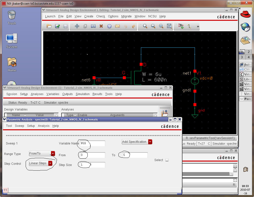
Finally,
select Analysis and Start, in the Parametric
Analysis window, to see the MOSFET IV curves below.
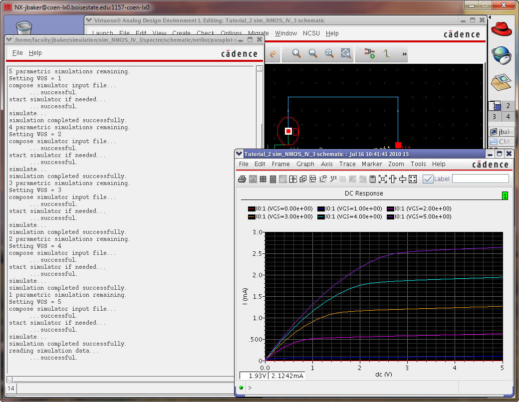
Note
that we could have avoided making the symbol view so
that plotting these curves would take less effort.
Why
we chose this path will become clearer later in the
tutorial (having a symbol allows us to simulate either the schematic or
extracted, from layout, views)
Quit
the ADE and Save the State (okay to overwrite existing
state).
Close
the schematic of sim_NMOS_IV_3 (close all Cell Views).
We
are now ready to lay out this cell and simulate it.
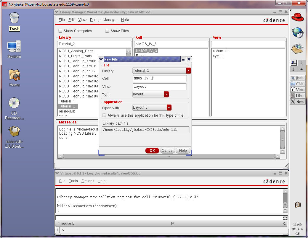
Create
a layout view for NMOS_IV_3 (not
sim_NMOS_IV_3)
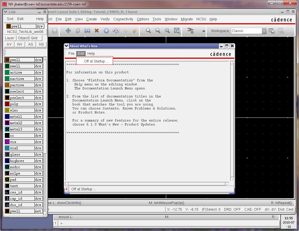
We
get that pesky start-up Window again even though we set it
to be Off at Start-up before (below).
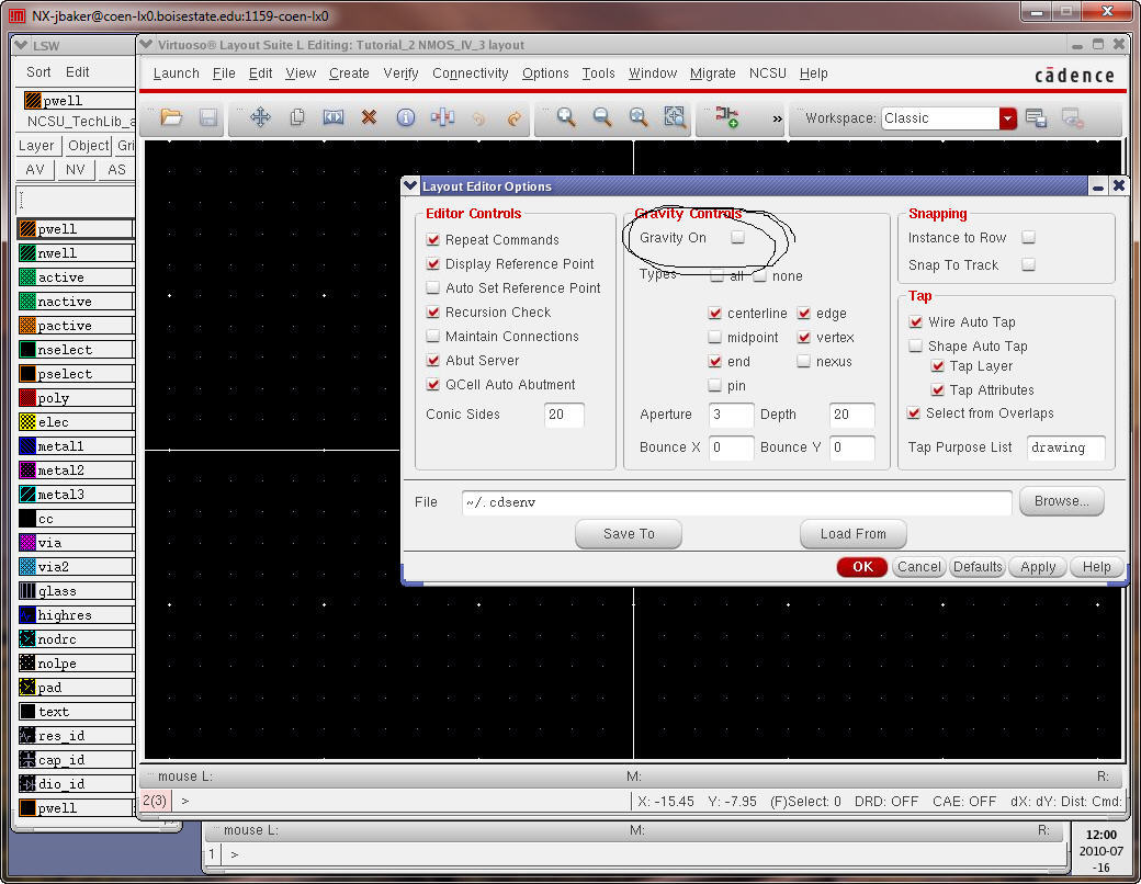
We’ll
also see that our Editor Options, E,
and Display Options, e,
(also below) have reverted back to the original states.
Change
the values back to those seen below.
 e
e
After
pressing e
we get the following.
To
ensure that the options are remembered Save To File (the
CDS, Cadence Design System, Environment,
.cdsenv) as seen below
(saved in $HOME, aka, ~/).
Note
that to see the Save To button you may need to re-size
the Display Options dialog window.
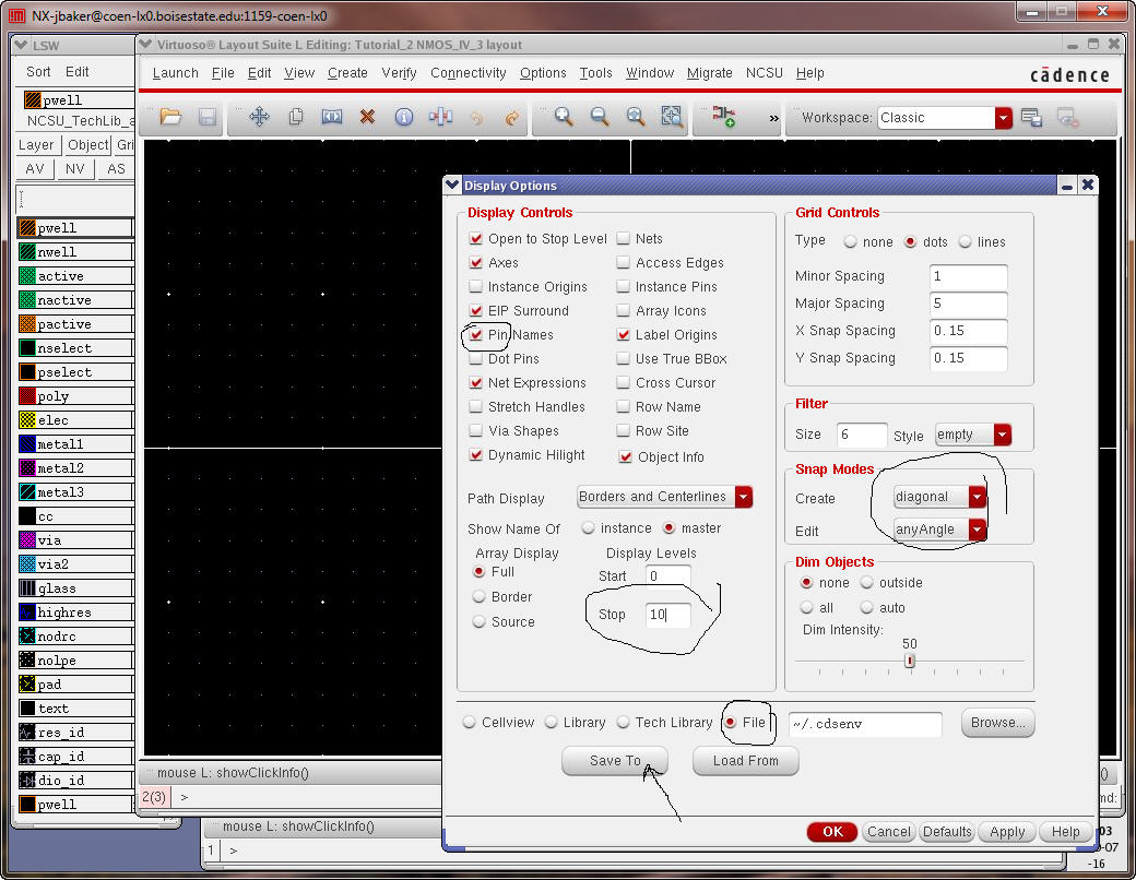
When
finished hit OK and re-size the layout window as seen
below.
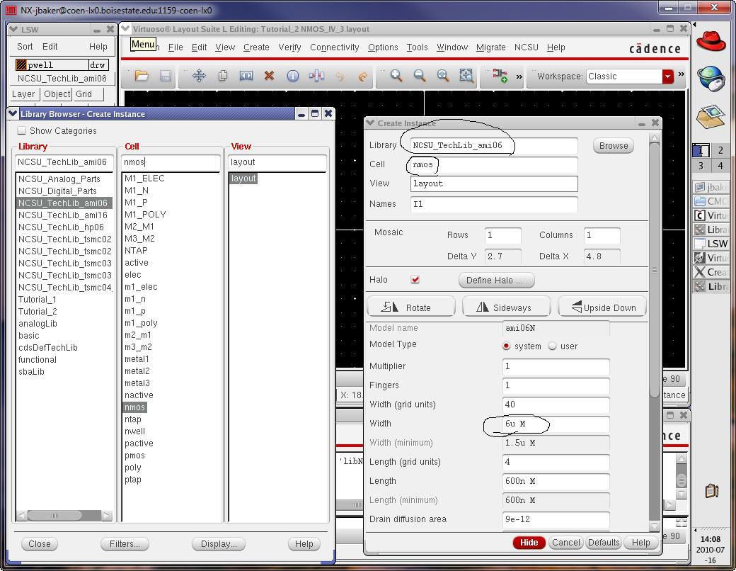
Next
instantiate an nmos
device
that is 6 um wide and 600 nm long.
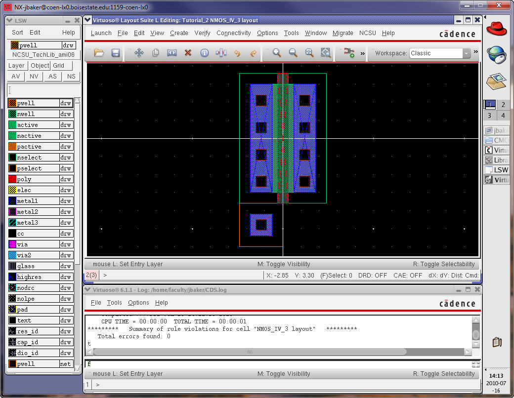
Next
instantiate a ptap cell
(metal1 connection to p+) in the p-substrate so you get something that
looks
like the following.
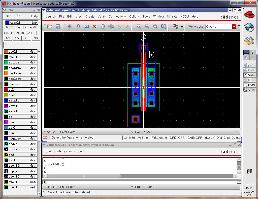
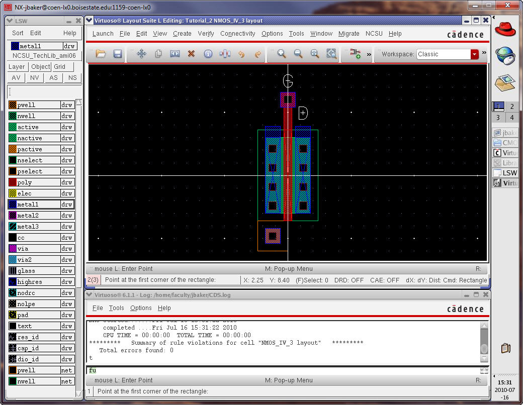
DRC
the layout (Verify -> DRC then OK).
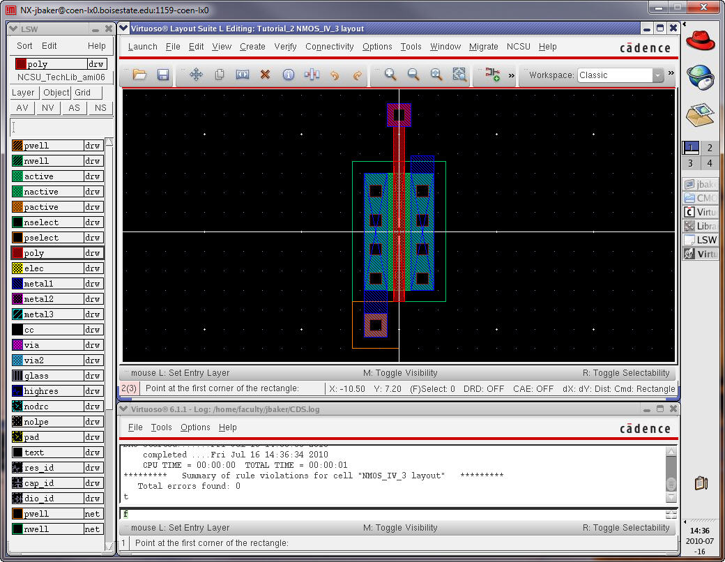
Next
add rectangles on the metal1 layer to connect the source
to the p-substrate and to the drain.
Also
add a metal1-connection-to-poly cell (m1_poly) and a
poly rectangle to connect the gate to m1_poly.
DRC
your layout.
Pressing
e and
then setting the display level stop to 0 we can see the rectangles and
cells.
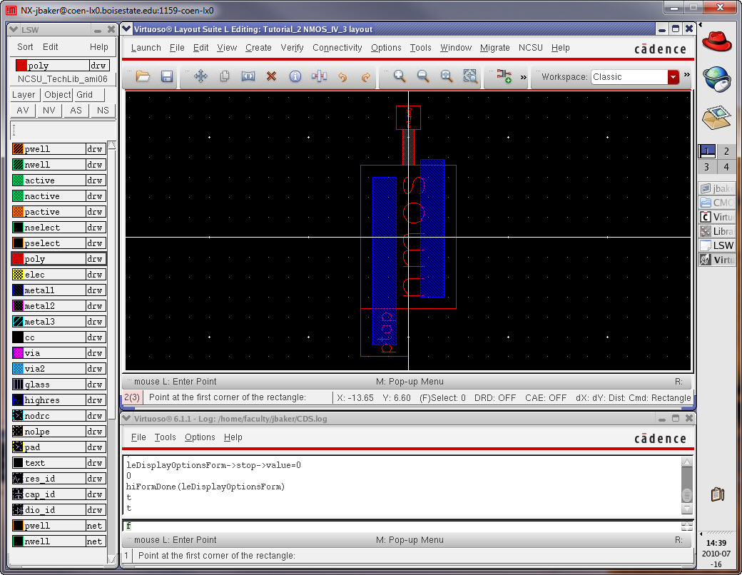
Set
the display stop level back to 10.
Add
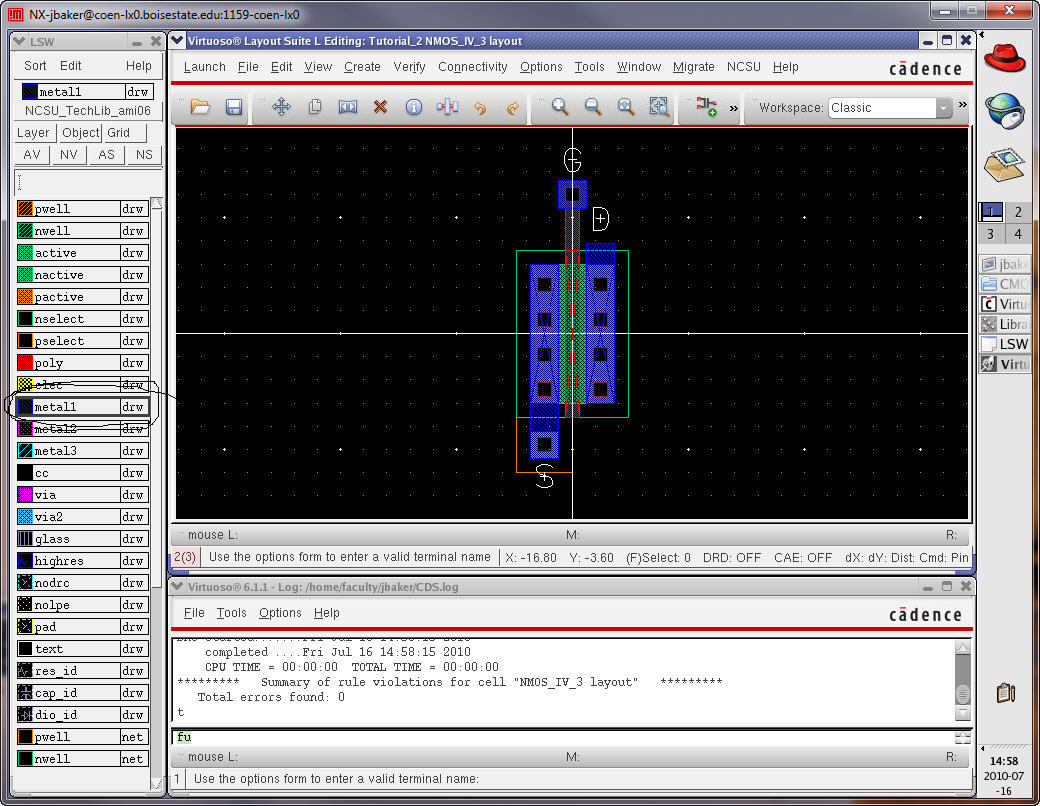
D, G, and S Pins on metal1 as seen below.
Ensure
“Display Pin Name” is selected and I/O type is inputOutput
to match the pins in the schematic.
Draw
the pins so they overlap the metal1.
DRC
the layout to ensure no errors (fix errors if you find
them).
Save
the cell view.
Next
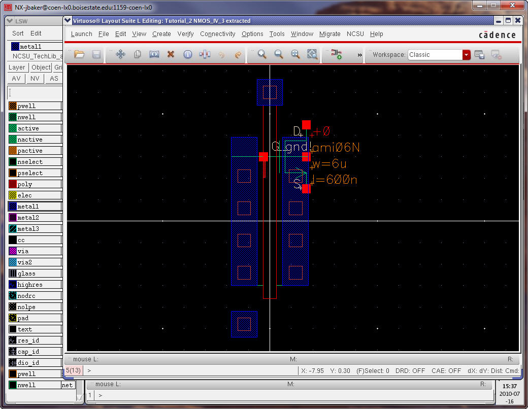
Extract the layout (Verify -> Extract).
Using
the Library Manager open the extracted cell view
(NMOS_IV_3).
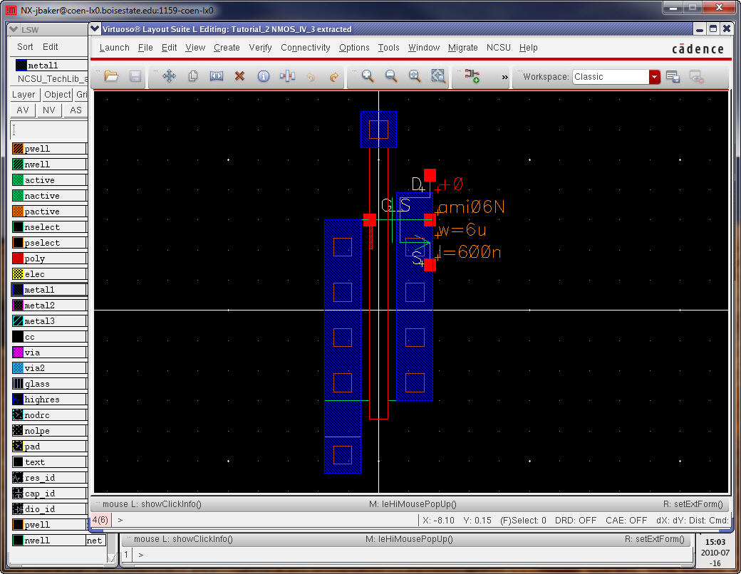
Notice
that the symbol displayed here has 4 terminals, not
the 3-terminal transistor we used in the schematic (where it’s assumed
the
p-substrate is tied to gnd!)
Next
run an LVS (Verify -> LVS).
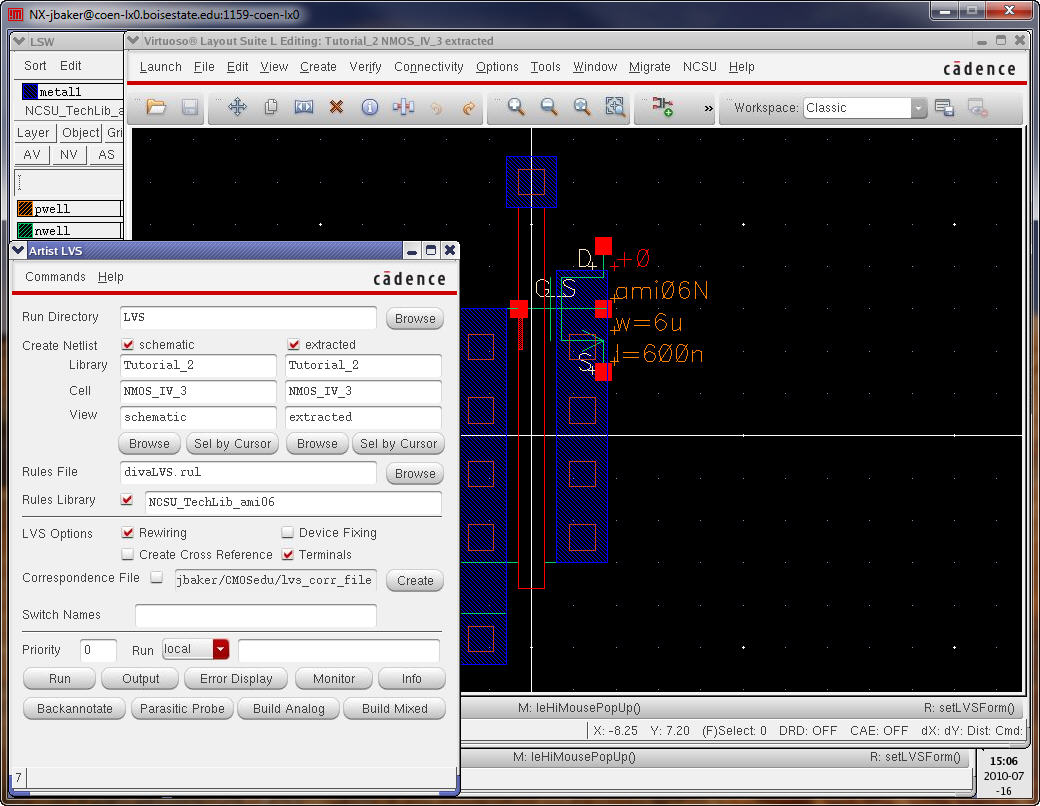
After
hitting Run you will be notified that the job failed.
Click OK.
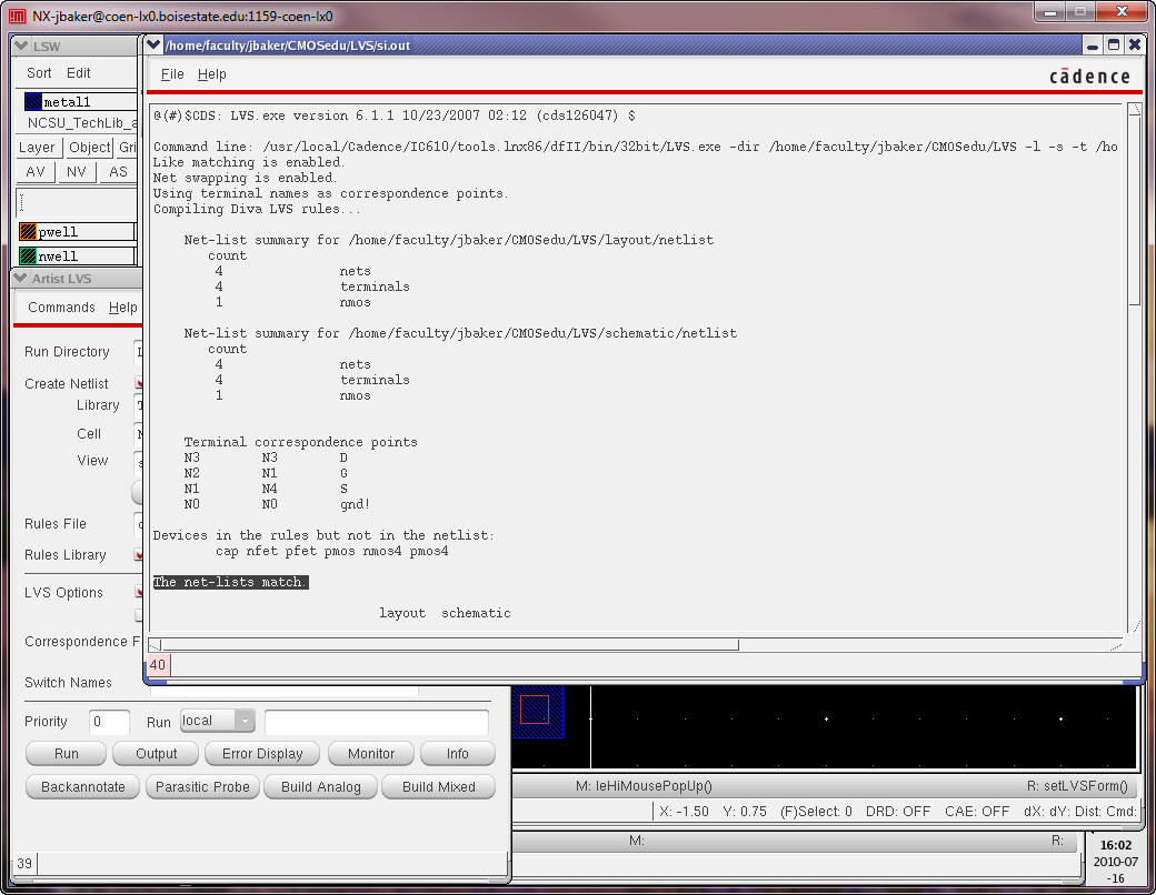
In
the Artist LVS window click on Info and then Log File to
get, after scrolling down, the following.
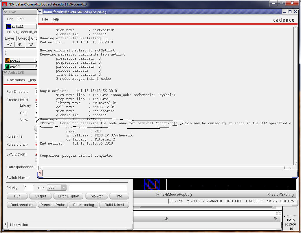
The
error is related to the bulk (p-substrate) connection for
the NMOS. Again, as mentioned above when the 3 terminal MOSFET symbol
is used
it’s assumed
that
the bulk is tied to gnd!
for
an NMOS device and vdd!
for a PMOS device.
Let’s
modify the layout as seen below.
Delete
the metal1 rectangle and pin connecting the S to the
bulk (ptap) as seen
below.
Next,
add metal rectangles on metal1 over the S and B metal.
Next
add Pins, again make the Pin the same size as the metal1
rectangles (note that that making the Pins the same size is not a
requirement).
Save
your layout and DRC it.

Once
again run the Extractor and open the extracted view
using the Library Manager.
Notice
that it’s basically the same view except that now the
bulk of the NMOS devices is connected to gnd!
Again
we get a failed LVS run and the error “*Error*
Could not determine the node name for
terminal 'progn(bn)'.” It
looks like LVS wants us to use
a
4-terminal transistor in our schematics! Let’s try this.
Close
all Cell views.
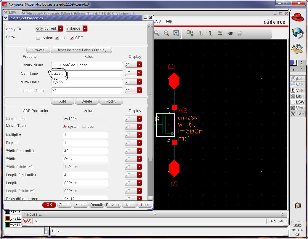
Open
the Library Manager and rename NMOS_IV_3 to NMOS_IV.
Also,
rename sim_NMOS_IV_3 to sim_NMOS_IV
Now
open the schematic view of NMOS_IV and change the NMOS
symbol as seen below.
Move
the symbol and then add the wire and label as seen
below.
It
may also be good to simulate this schematic (using the sim_NMOS_IV cell), following the
steps seen above, to
ensure that we still get the NMOS’s IV curves.
Open
the extracted view and perform an LVS.
Ensure
that you select the correct cell, see circled text
below.
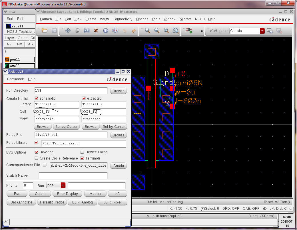
And
now!
Okay,
let’s simulate the extracted layout.
Open
the schematic view of sim_NMOS_IV
and then Launch the ADE L.
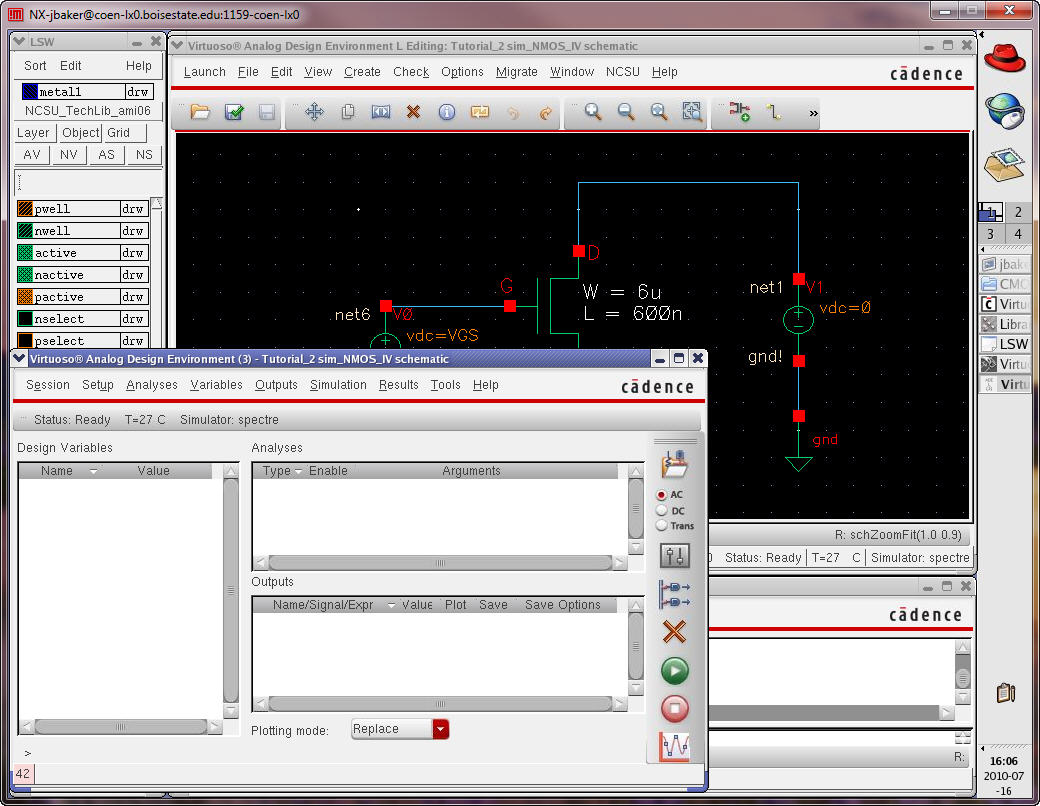
Go
to Session -> Load State then select Cellview
and OK.
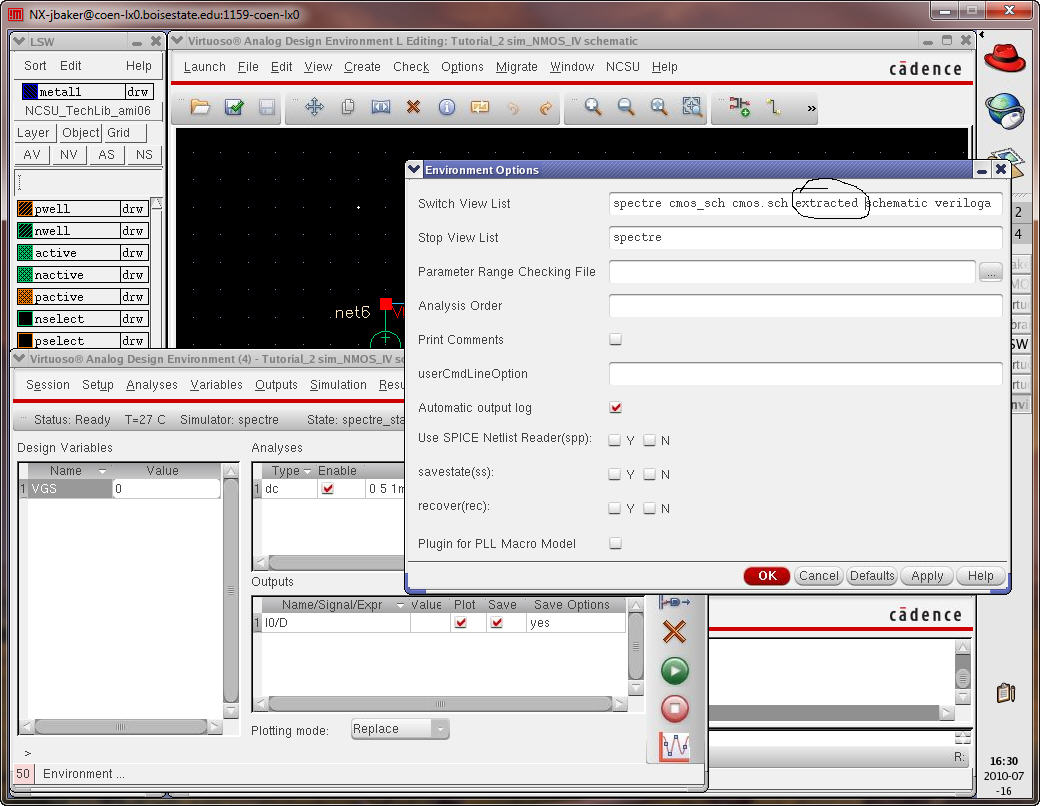
Then,
on the ADE menu, select Setup -> Environment and
enter extracted before schematic as seen below (so the extracted view
is used
before the schematic
view
when running the sim).
An
important note: if you save the state with extracted view
in front of schematic view you may get frustrated when you change your
schematic and the
simulation
doesn’t change!
Next,
again as we did earlier, select Tools -> Parametric
Analysis, enter the values seen below and then select the menu items
Analysis
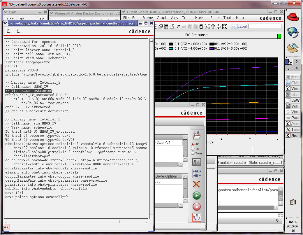
-> Start to simulate.
Just
to ensure that we are simulating the extracted view and
not the schematic view go to the ADE and select Simulation -> Netlist -> Display (see
below).
Let’s
repeat these steps for the PMOS device but in a much
more concise manner (since now we are getting the hang of things and
have made
mistakes and fixed them).
Create
a schematic Cell View called PMOS_IV with 4 pins as
seen below. Note the W and L of the PMOS device.
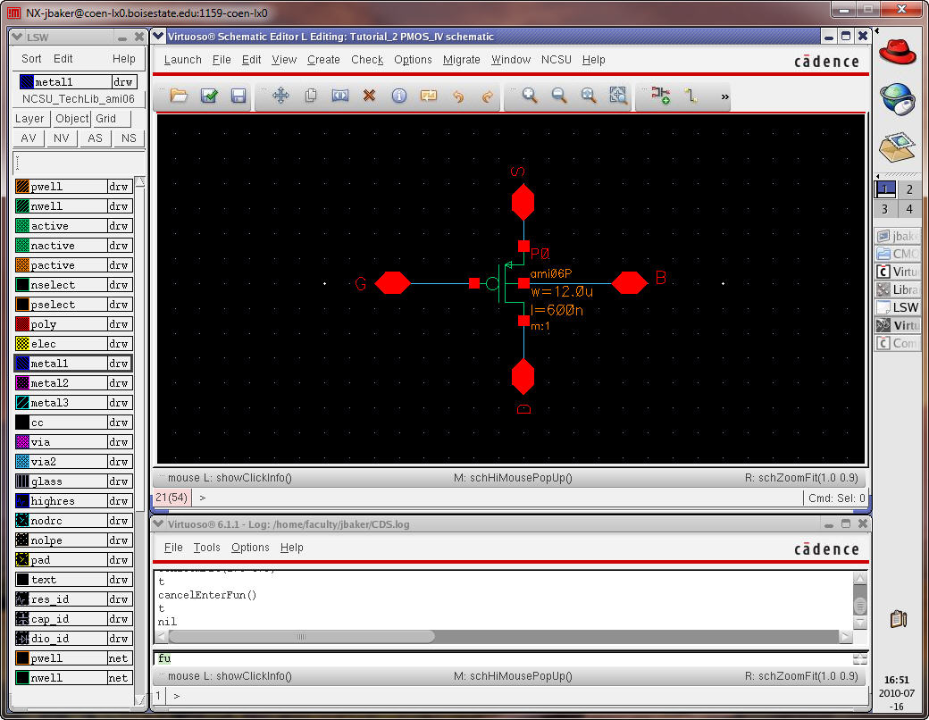
Check
and Save the schematic.
Next
create a symbol for the schematic.
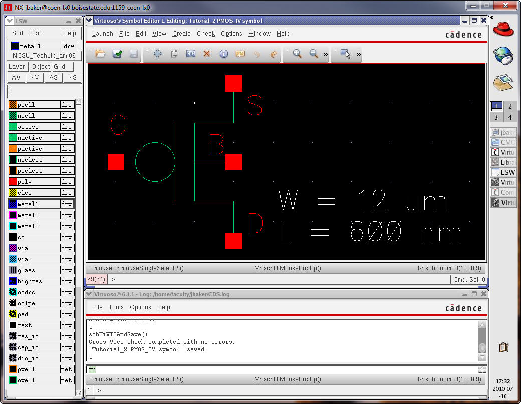
Check
and Save the symbol.
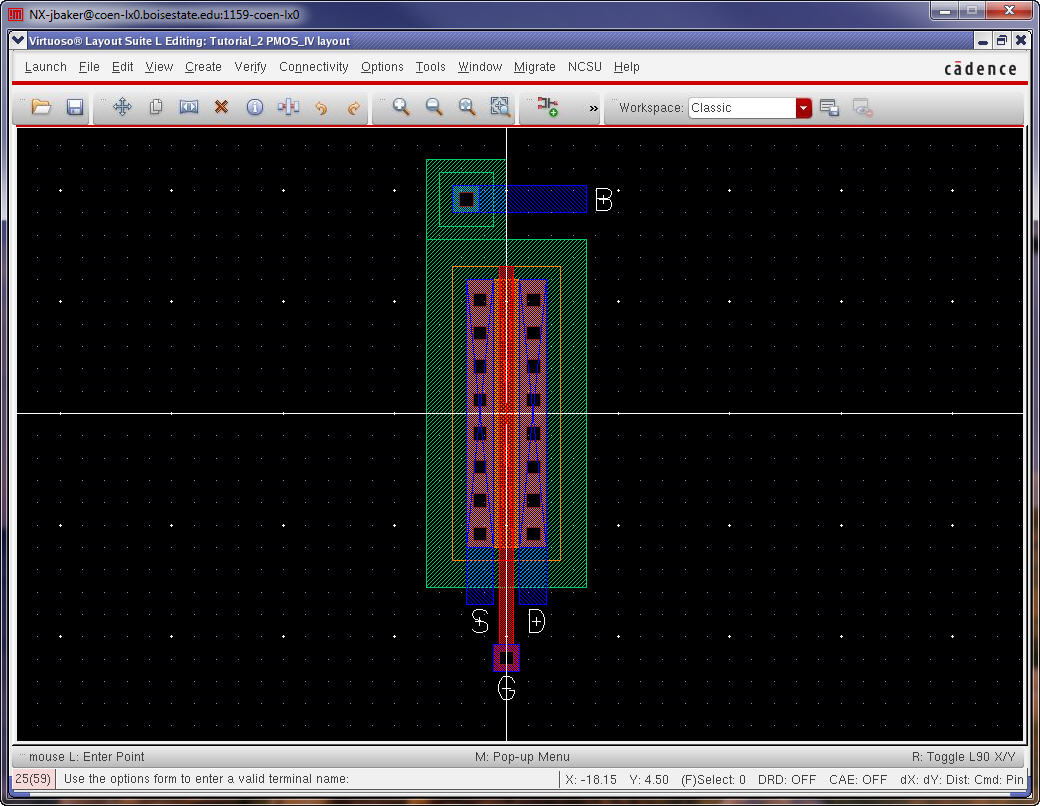
Next
create the layout (pmos
cell
and ntap).
DRC
and Save the layout.
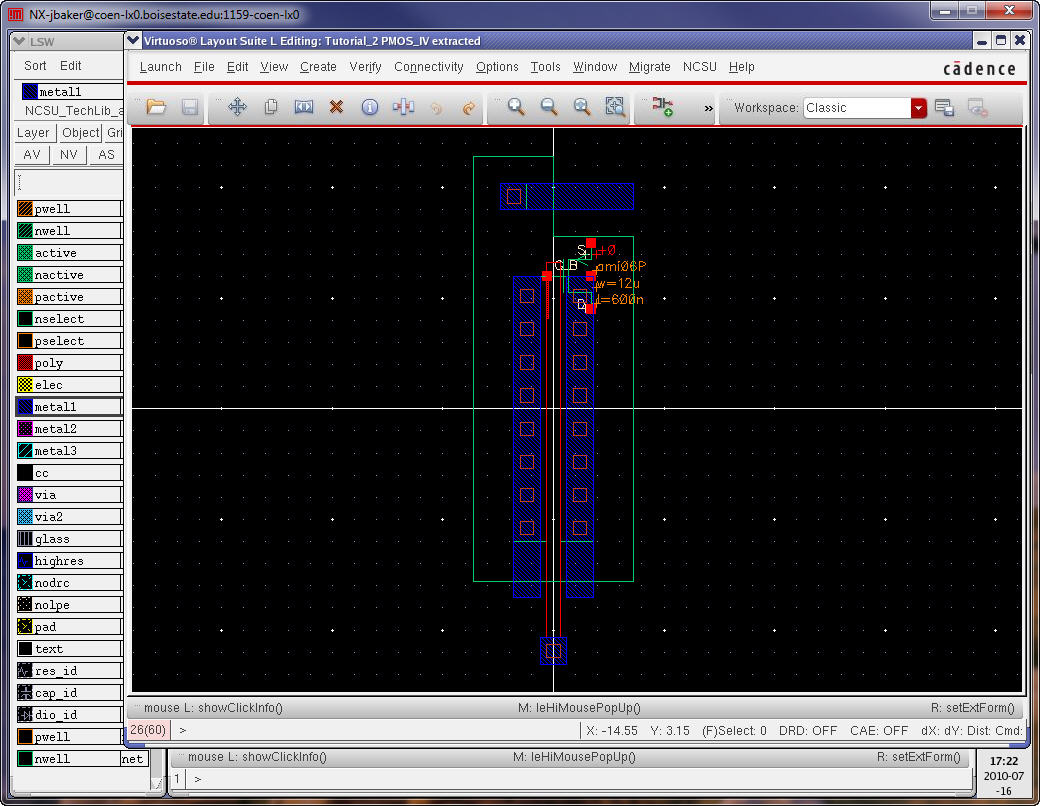
Next
Extract the layout.
Open
the extracted view in the Library Manager.
Save
and close all open Views.
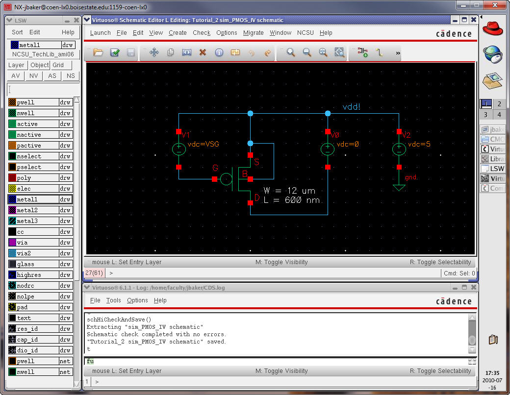
Next
create a cell called sim_PMOS_IV
and draft the following schematic.
Note
the value of /V1 is VSG (not VGS as we used in the NMOS sim).
When
finished Check and Save.
We
are now ready to simulate this design.
Launch
the ADE then go to Setup -> Model Libraries and
select the PMOS models for AMI06 (setting the models is important!).
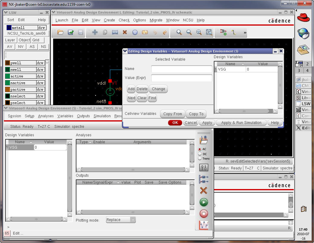
Variables
-> Edit and Add VSG with a value of 0 (not VGS)
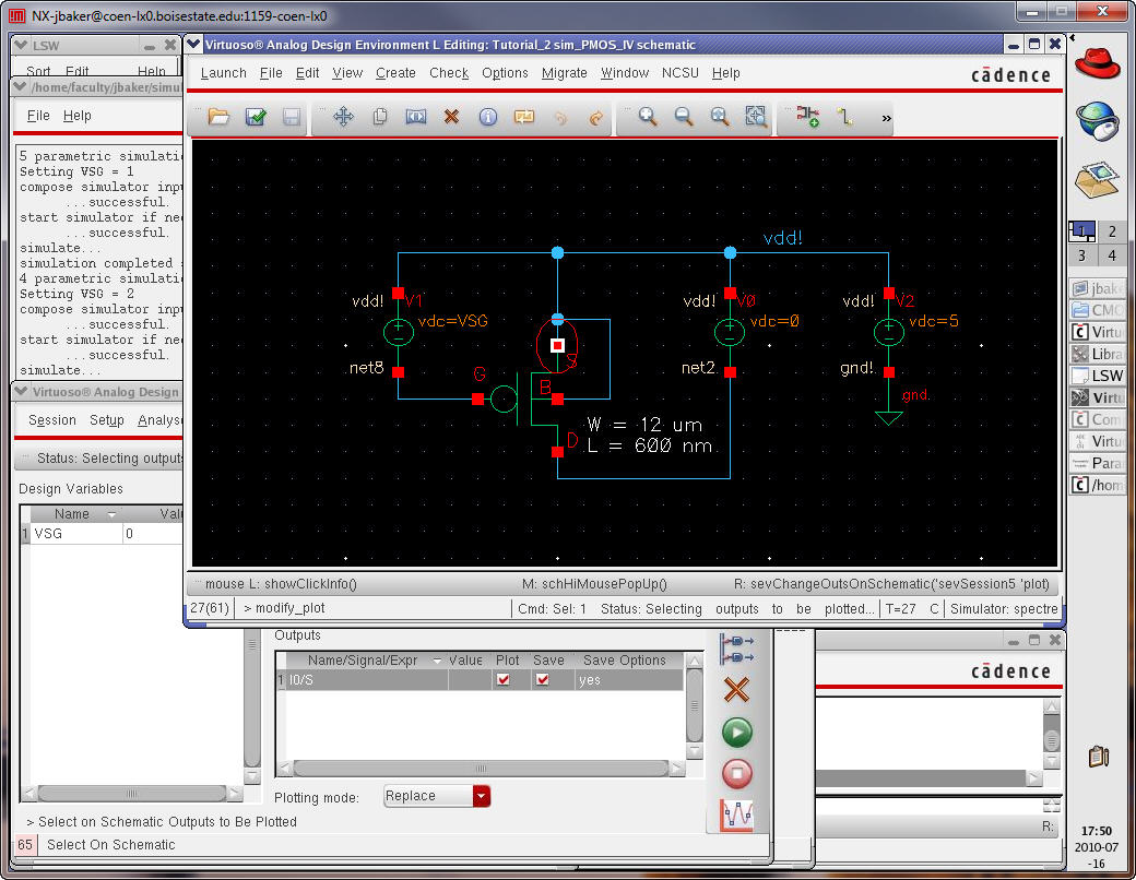
Next
select Outputs and the source terminal of the
transistor.
Ensure,
as seen below, that both Plot and Save are selected.
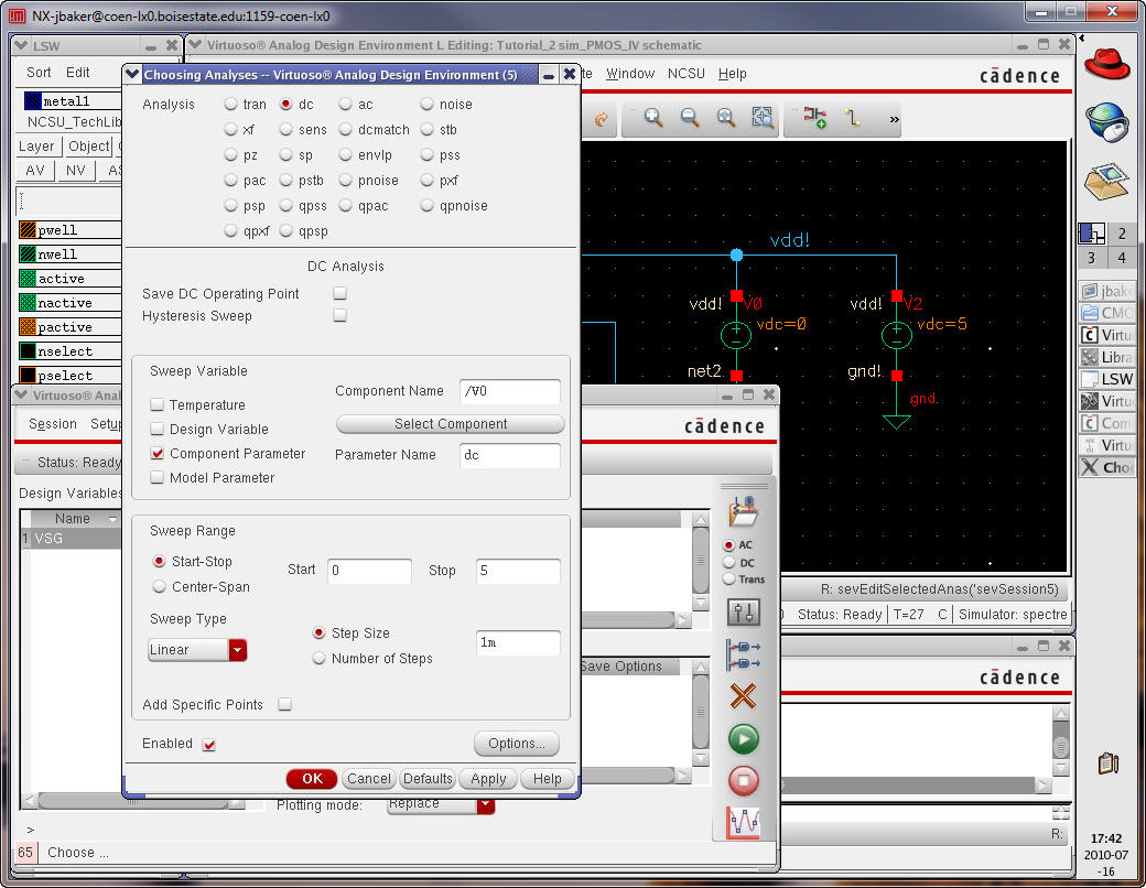
Select
Analyses and enter the following.
Note
that /V0 is VSD.
Also
note that the vdd!
Source,
that is /V2, really doesn’t do anything. It could be zero but we
include it
since it’s common to connect the S/B to vdd!
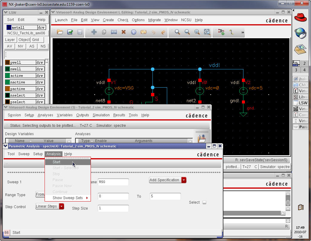
Save
the state in the cellview.
Then
go to Parametric Analysis and enter the values seen
below (again, it’s VSG not VGS).
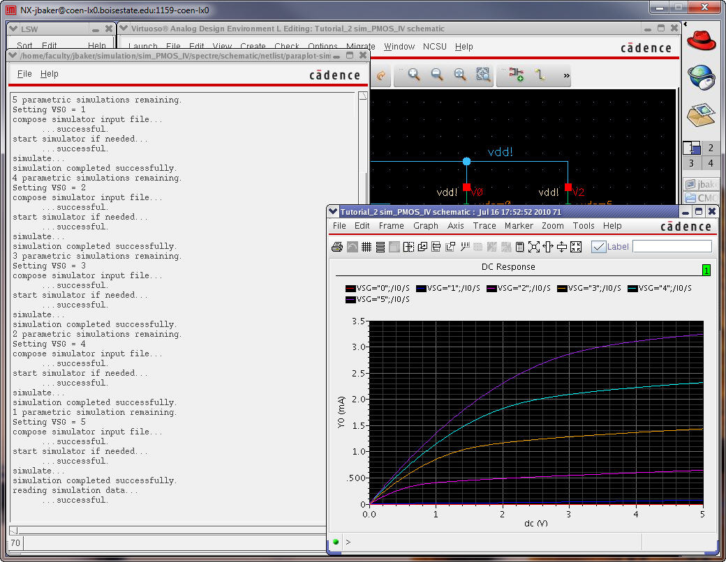
Starting
the analysis results in the following. Note that
this is the simulation of the schematic.
Now
let’s simulate the extracted layout.
In
the ADE go to Setup -> Environment and add extracted
before schematic.
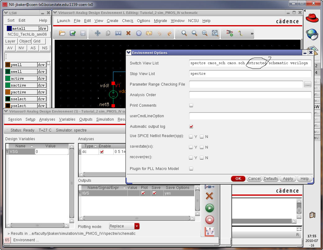
And
we get the same thing as with the schematic.

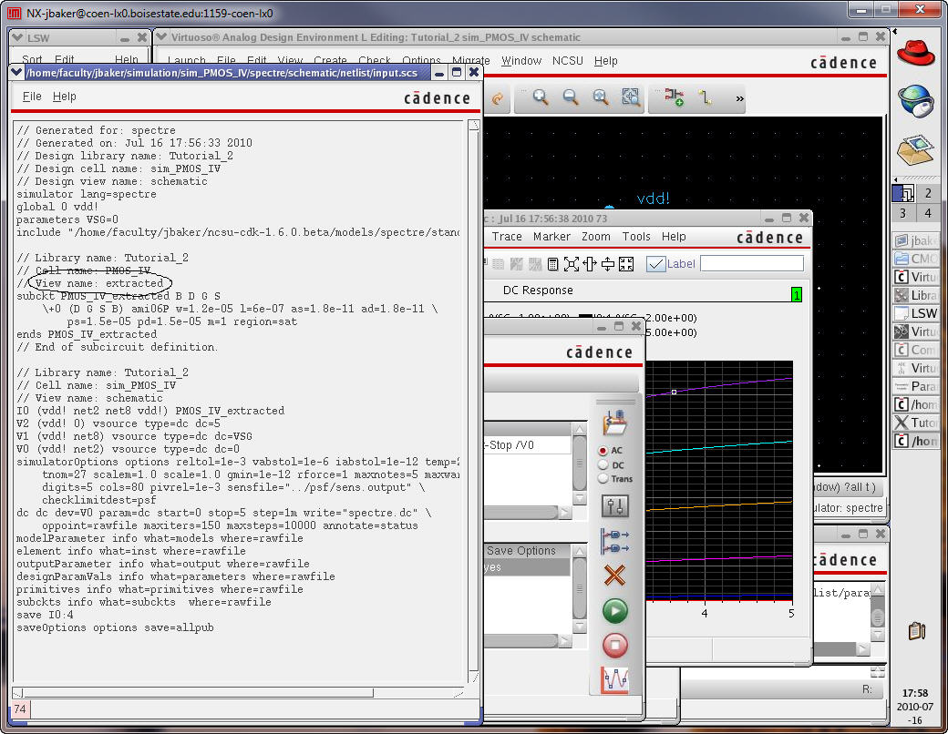
Just
to verify that we are simulating the extracted view go
to ADE Simulation -> Netlist
-> Display.
An
important note: if you save the state with extracted view
in front of schematic view you may get frustrated when you change your
schematic and the
simulation
doesn’t change! The simulator simulates your old
extracted view instead of your modified schematic view.
Save
the state and close everything. This concludes Tutorial
2.
For
your reference the Tutorial_2 directory is available
in Tutorial_2.zip.