Cadence
Design System
Tutorials
from CMOSedu.com (Return)
Tutorial
6 – Placing circuit layouts
in a padframe for
fabrication
In
this tutorial
we’ll place the R_div,
NMOS_IV, PMOS_IV, inverter,
nand2, and ring oscillator that we laid out
in
the earlier tutorials in a padframe
for fabrication through MOSIS.
Note
that we won’t include a buffer to drive the large,
around 30 pF, off-chip load capacitance
from
the scope probes, packaging, and test board needed to
test the chips.
What
this means is that if the chip we lay out here is
fabricated it’s likely that attempting to measure the
oscillation
frequency, or the gate delay, with a scope probe
will result in drastically different results than the
simulations.
It’s likely that measuring the ring oscillator
frequency will actually result in killing the oscillations
(see
the CMOS
book for details on the use of output
buffers to drive off-chip loads).
Okay,
let’s begin by copying the library, Tutorial_5, into a new library
called
Tutorial_6.
Ensure,
when you copy, that “update instances” is selected so that the new
library
doesn’t reference cells in the other libraries.
As
always, put the new library in $HOME/CMOSedu
We
are using
On
Semiconductor’s C5
process for fabrication through MOSIS.
Further,
this process uses the MOSIS scalable CMOS (SCMOS) submicron design rules with lambda
of 300 nm (technology
code SCN3ME_SUBM at 0.3).
A
“tiny chip” fabricated in this process via the MOSIS Educational
Program (MEP)
measures, at most, 1.5 mm by 1.5 mm.
Information
about the MOSIS Educational Program (MEP) is found here.
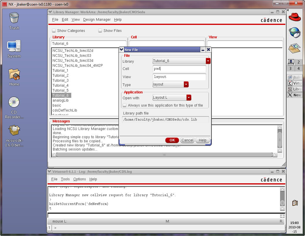
Create
a new layout cellview
called
pad.
If we have 12 pad
cells on a side (10 plus two corners) then each cell must be 1.5mm/12
or 125
um.
In order to ensure
this pad falls on the 0.15 um grid let’s reduce the pad cell size to
120 um.
This also ensures
that the final chip size is smaller than the 1.5 mm square size we are
allowed.
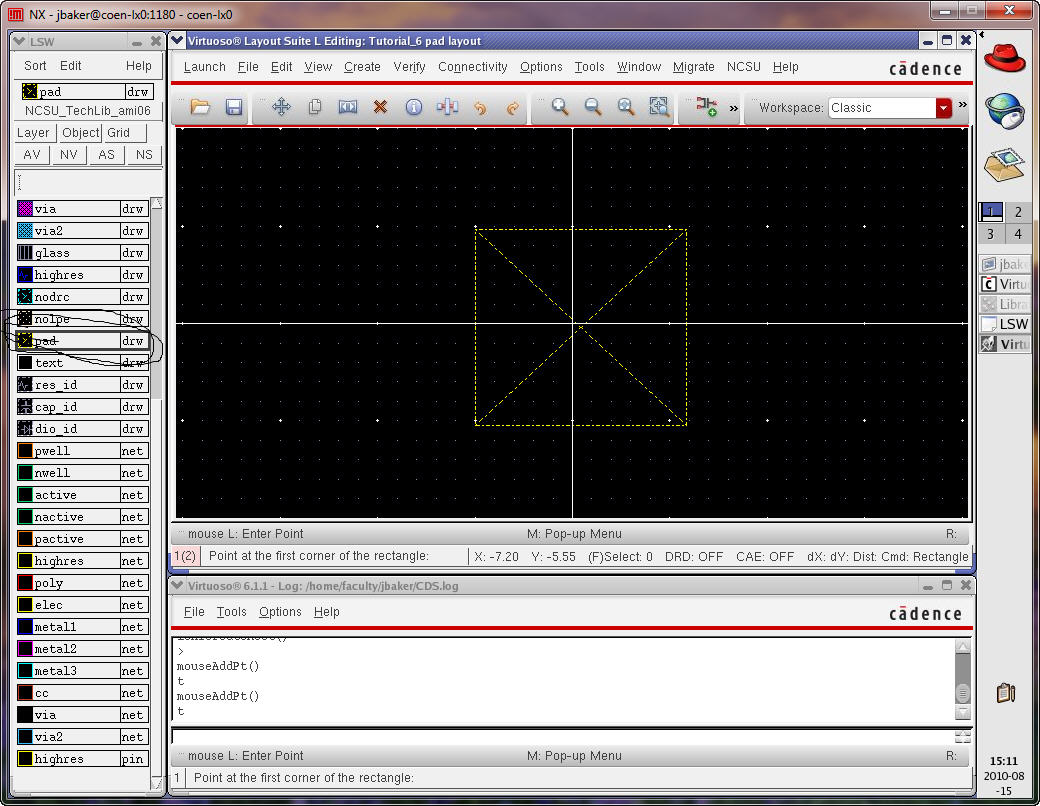
Select the pad
layer and add an arbitrary size rectangle as seen below.
The pad layer has
no fabrication significance (so you really don’t need it).
The pad layer was
used by MOSIS to indicate the location of the pads (now the location of
the
glass layer, that is cuts in the passivation,
is
used).
We’ll use the pad
layer as an outline for the cell. We could also use the text layer for
a cell
outline.
Next edit the
rectangle’s properties so that it is 120 um square centered upon the
origin.
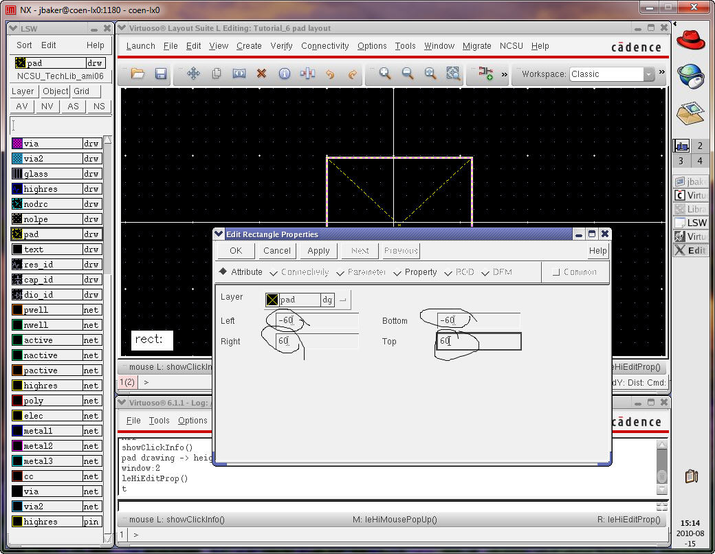
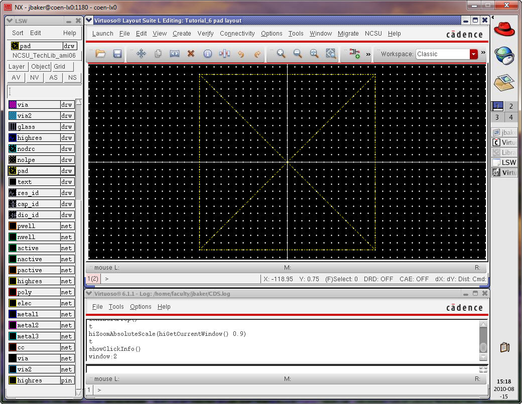
After fitting the
layout we get the following.
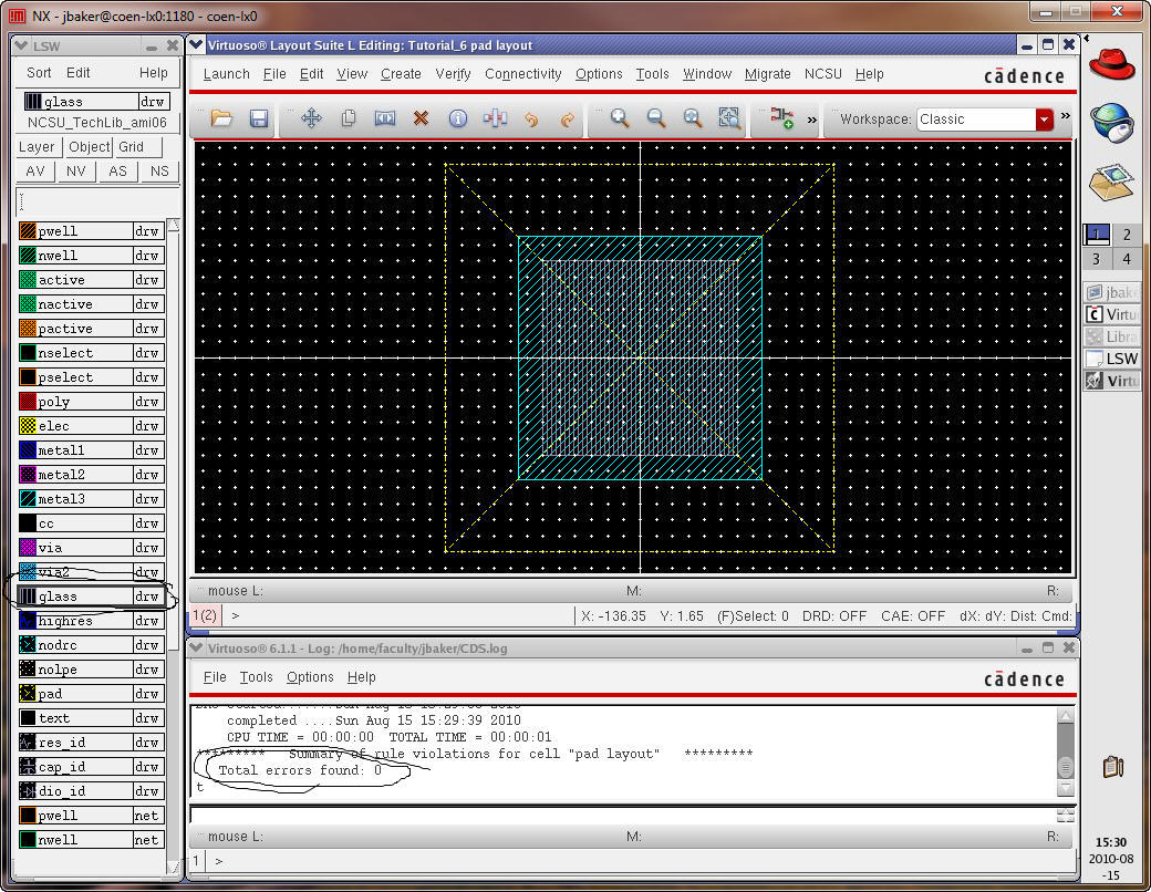
The
pad size (metal3) is 75 um square with overglass
(called glass, the opening in the top layer passivation)
6 um
smaller or a rectangle of 63 um.
Note
that both of these sizes, 75 and 63, are divisible by
0.15 (to avoid DRC errors by drawing layout off grid).
Add
two rectangles on these layers, centered around 0,0 to
get the layout of a pad.
DRC
the layout to ensure no errors. Save the cell.
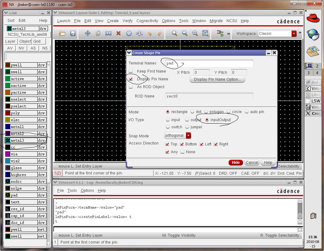
Next
instantiate a pin called “pad” with a direction inputOutput.
Use
the metal3 layer and place the pin over the entire metal3
rectangle (so the size is 75 um square).
Also
ensure Display Pin Name is selected.
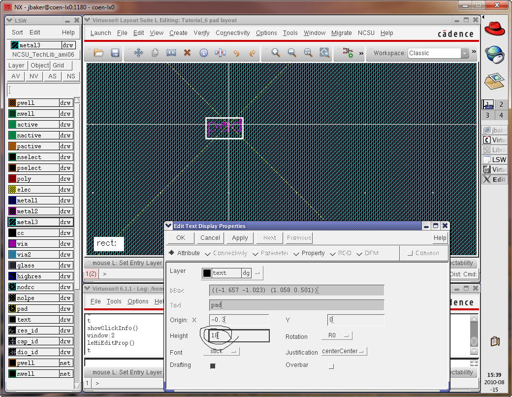
Zoom in and select the pin name and set it’s size to 18 um.
Note
that if you want to change the pin's name (grayed out below) you have
to select the rectangle on metal3 and *not* the pin name (text).
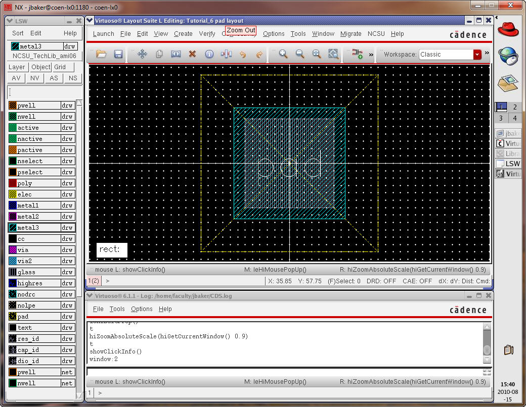
After
fitting the layout we get the following
Save
and DRC the layout.
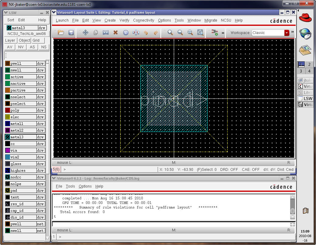
Next
create a layout cellview
called padframe and
instantiate the pad cell into
this new cell as seen below.
Add
a pin on the metal3 layer called pin<1> with a
direction of inputOutput.
Ensure
that Display Pin Name is selected.
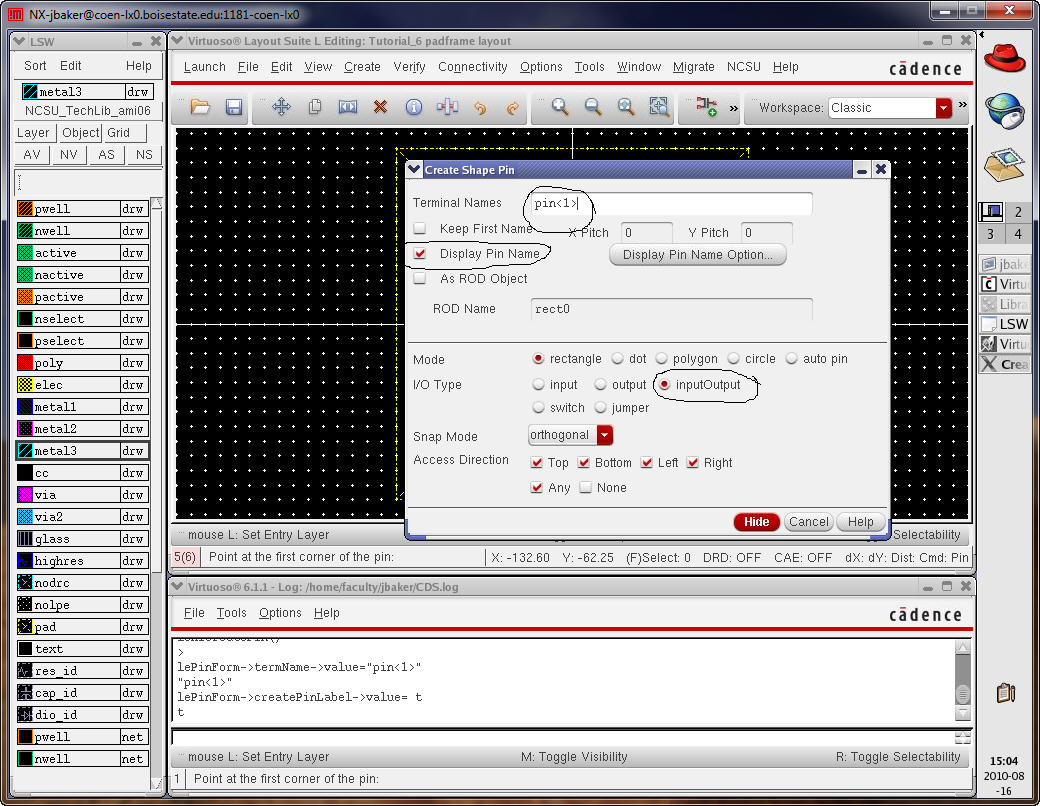
After
setting the pin<1> text size to 15 um we get
Next
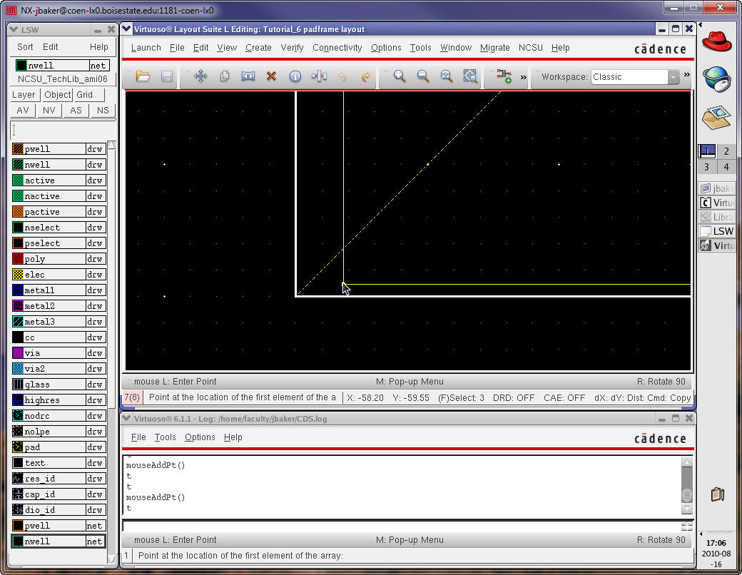
copy, c, the pad cell and pin then use F3 and set
the number of rows and columns to 12.
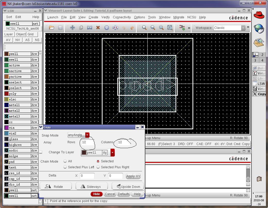
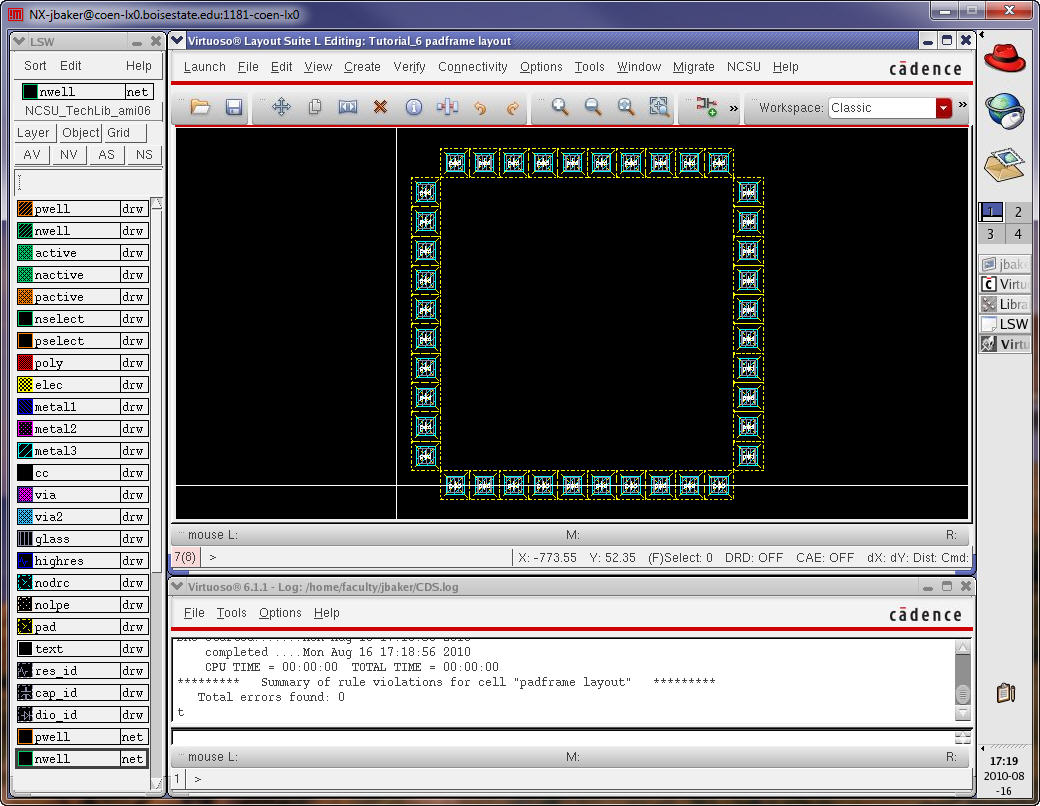
Select
the lower left corner of the layout.
Next
click on the lower right corner of the layout.
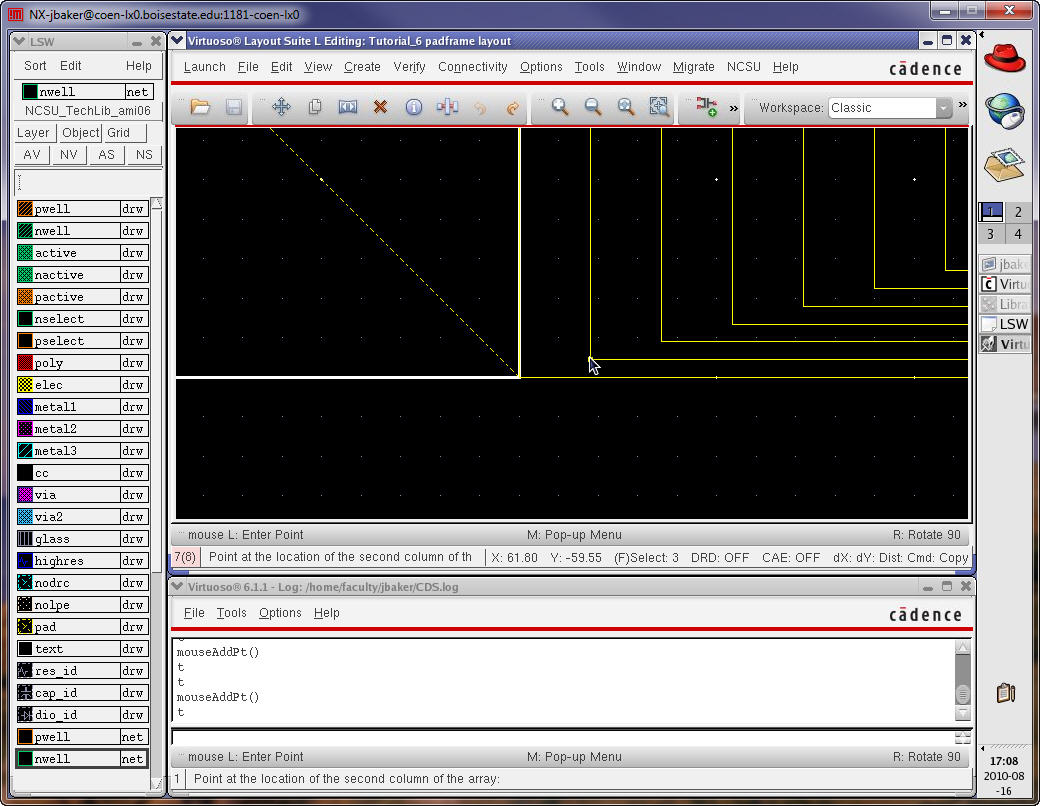
Following
this click in the lower right corner of the first
copied cell as seen below (zoom in to ensure that the cells are aligned
properly).
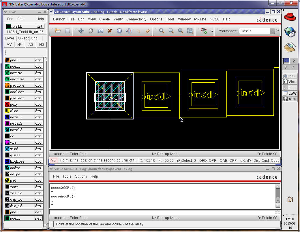
Finally,
click in the top, right, of the first copied cell to
get the layout seen below.
It’s
okay to make mistakes and try again (hit u to
undo and start over).
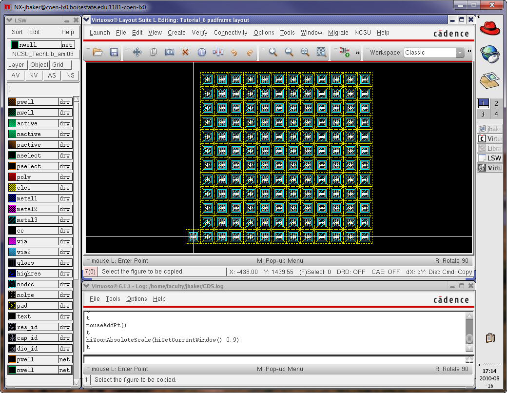
Delete
the middle, corner, and extra pads/pins to get the
basic padframe seen
below.
DRC
and save the layout of the padframe.
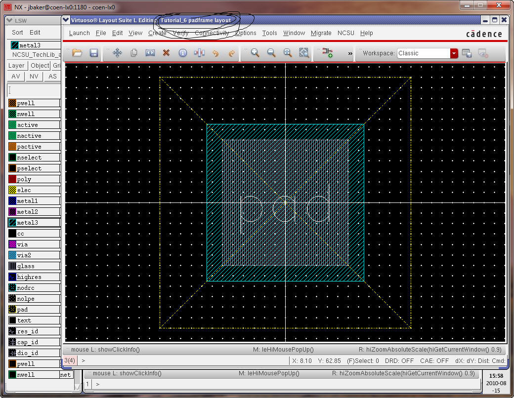
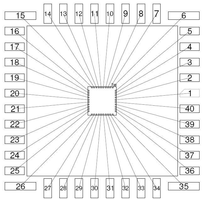
The
padframe is likely
bonded to
the package with the configuration seen below (the bonding diagram).
All
of the pins in the above layout are labeled pin<1>.
Change
the labels so that they match the bonding diagram seen
below.
For
example, pin 1 of the package corresponds to the 5th
bonding pad from the top on the right side of the die.
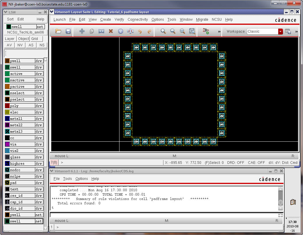
Remove
the pad layer from the pad cell.
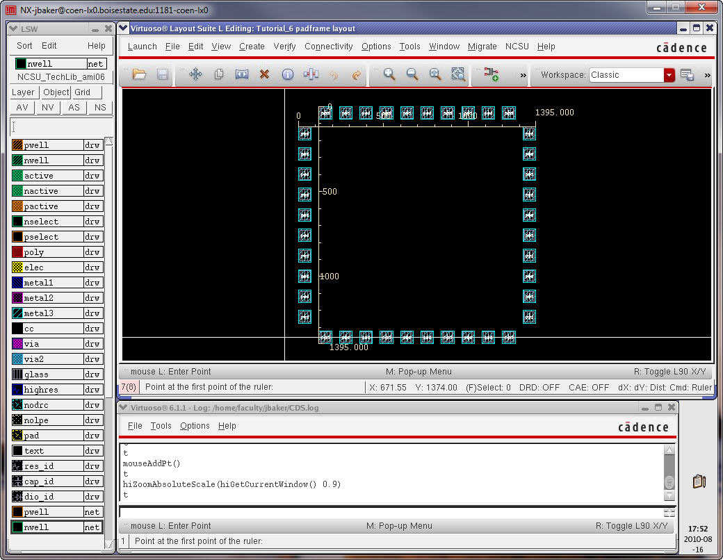
Let’s
measure the size of the padframe
(our chip) since we’ll need this information when we submit to MOSIS.
Using
the ruler we get the following sizes (1.395 mm square).
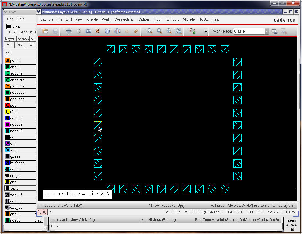
Before
leaving the layout view of the padframe
let’s generate the extracted view.
The
next thing we need to do is generate schematics for the
pad and padframe
layouts.
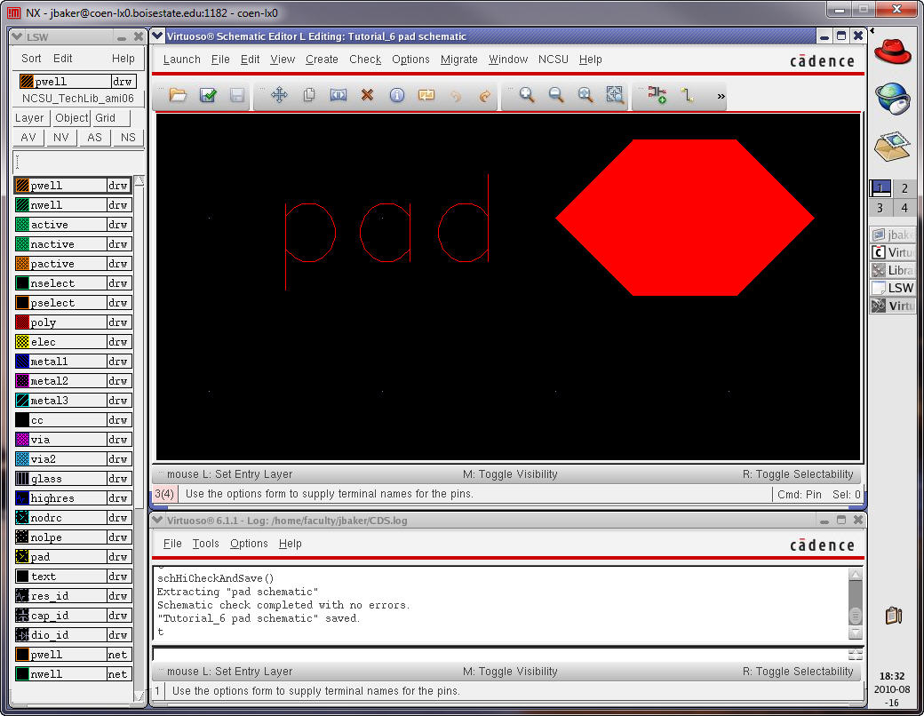
Generate
a schematic cell view for the pad cell and add a
pin, called pad, with a direction of inputOutput.
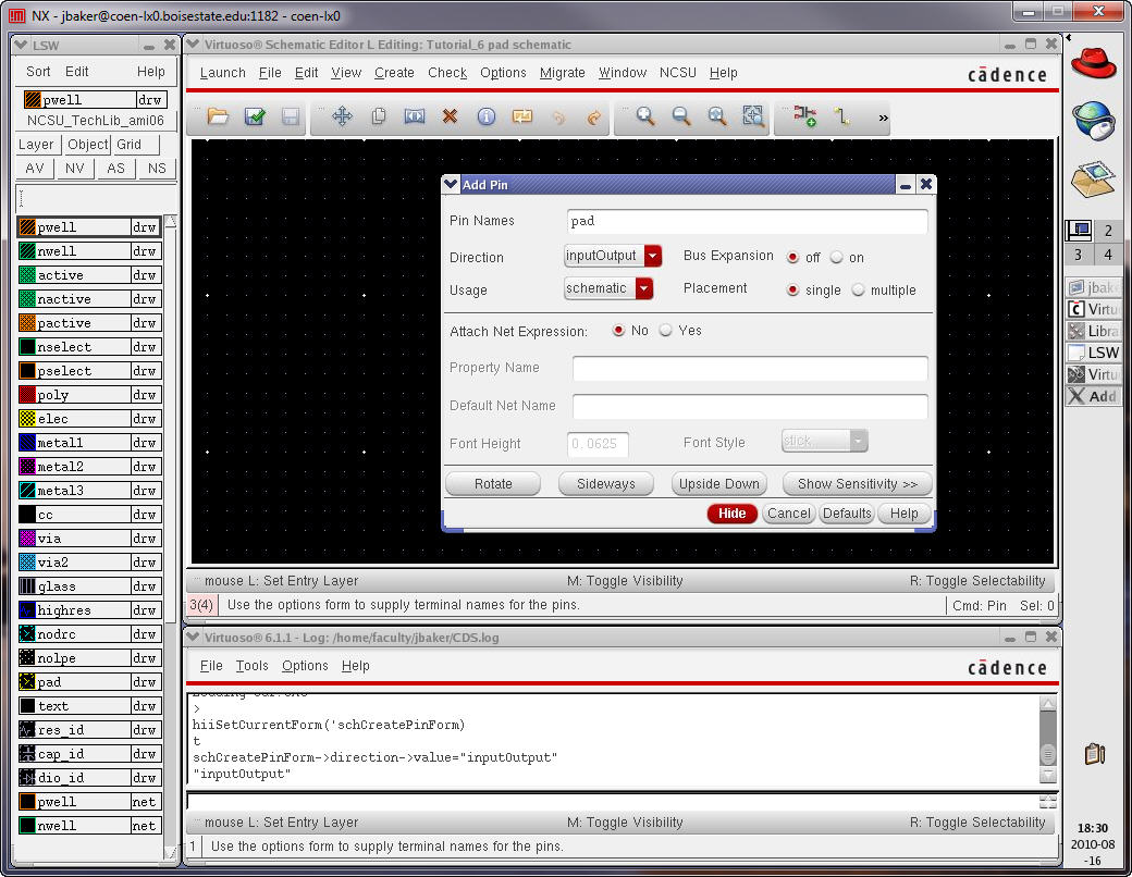
Check
and Save the schematic.
Use
Check -> find marker to ignore the warning that the
pin is floating.
Check and Save the schematic again.
Note
that an LVS can't be performed between the pad schematic and layout
since there are no devices (resistors, capacitors, transistors) in the
circuit.
Next
use Create -> Cellview
-> From Cellview
to create a symbol for the pad.
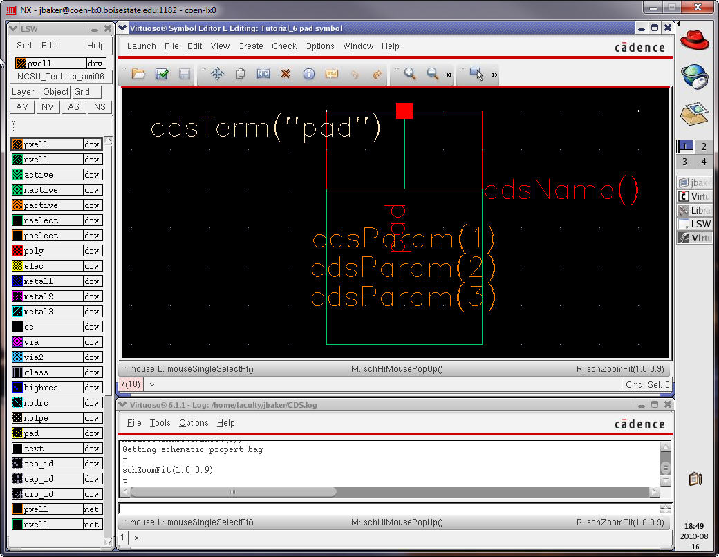
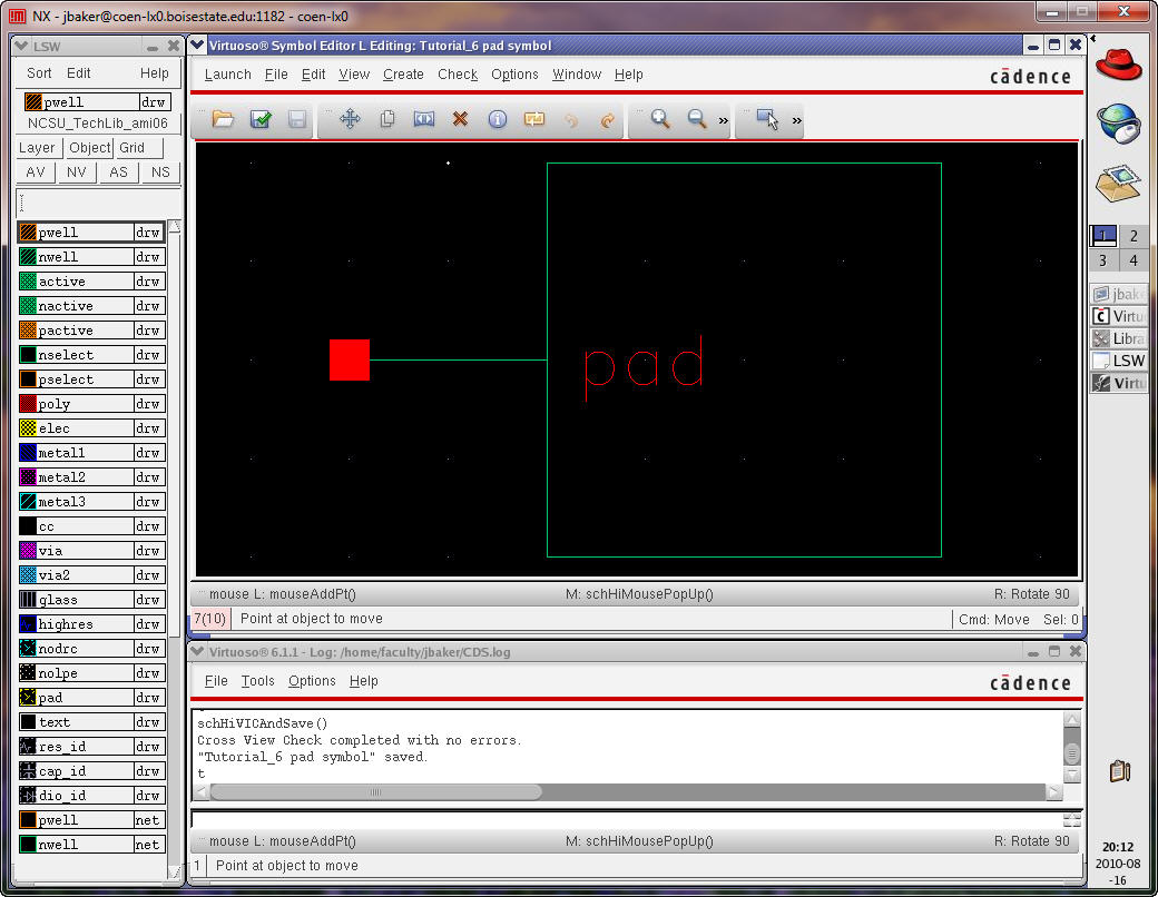
Delete
most items and rotate to get the following.
Save
the pad symbol cellview
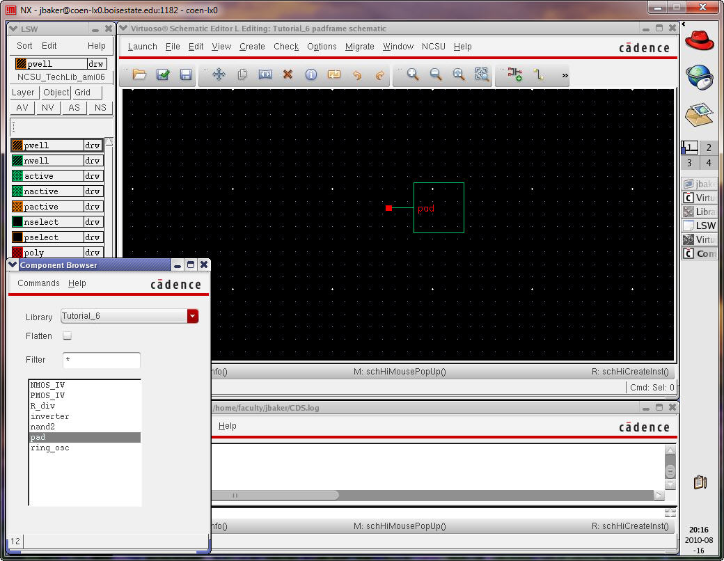
Create
a schematic cellview
for the
padframe and instantiate
the pad cell.
Array
the instance name and ensure the Display is set to
value as seen below.
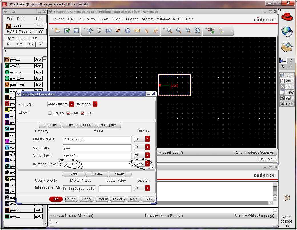
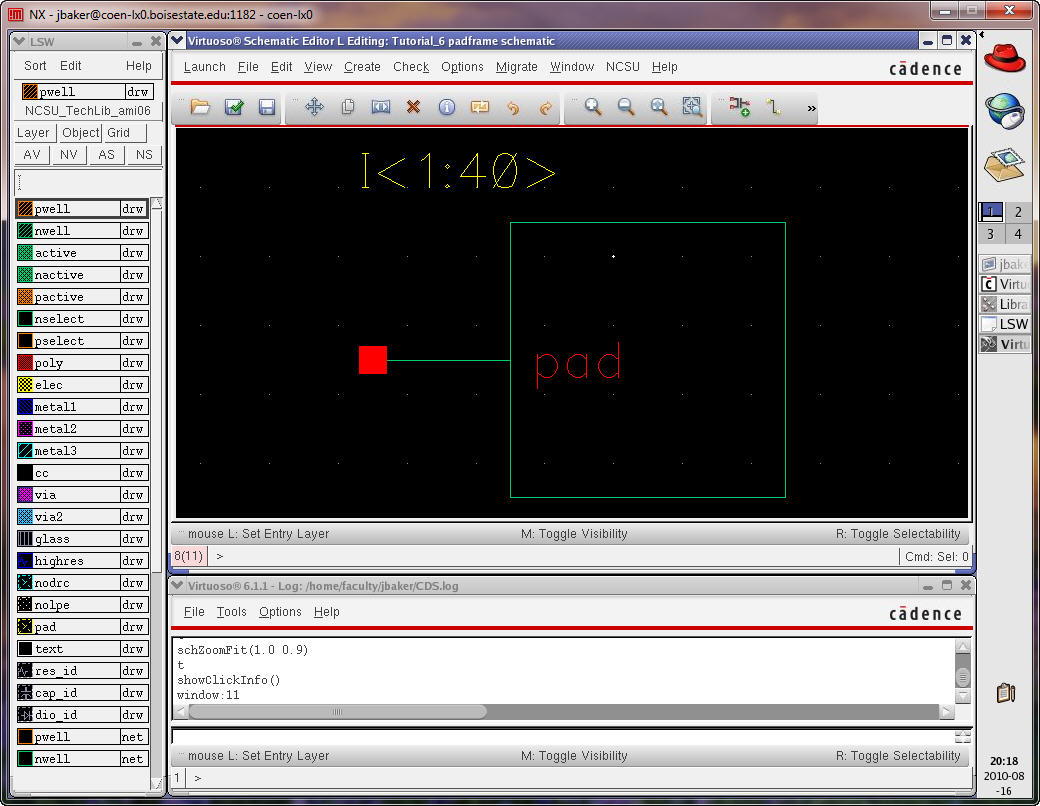
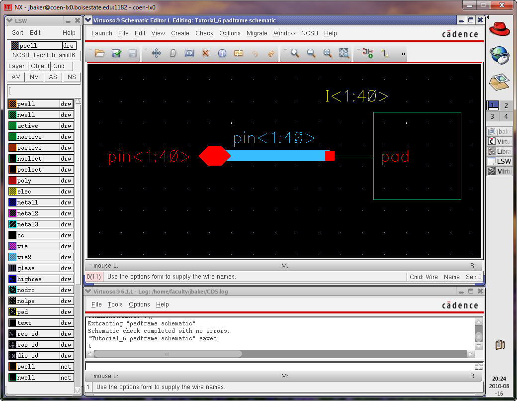
Add
a pin with a name of pin<1:40> and a direction of inputOutput to match the layout
of the padframe.
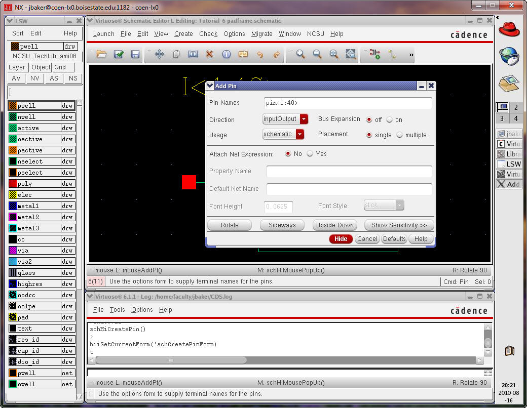
Add
a wide wire with a label pin<1:40>
Check and Save the schematic view of the padframe.
Note that an LVS can't
be performed between the padframe schematic and
layout since there are no devices
in the circuit.
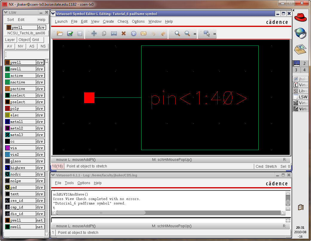
Next
let’s create a symbol for the padframe
using Create -> Cellview
-> From Cellview
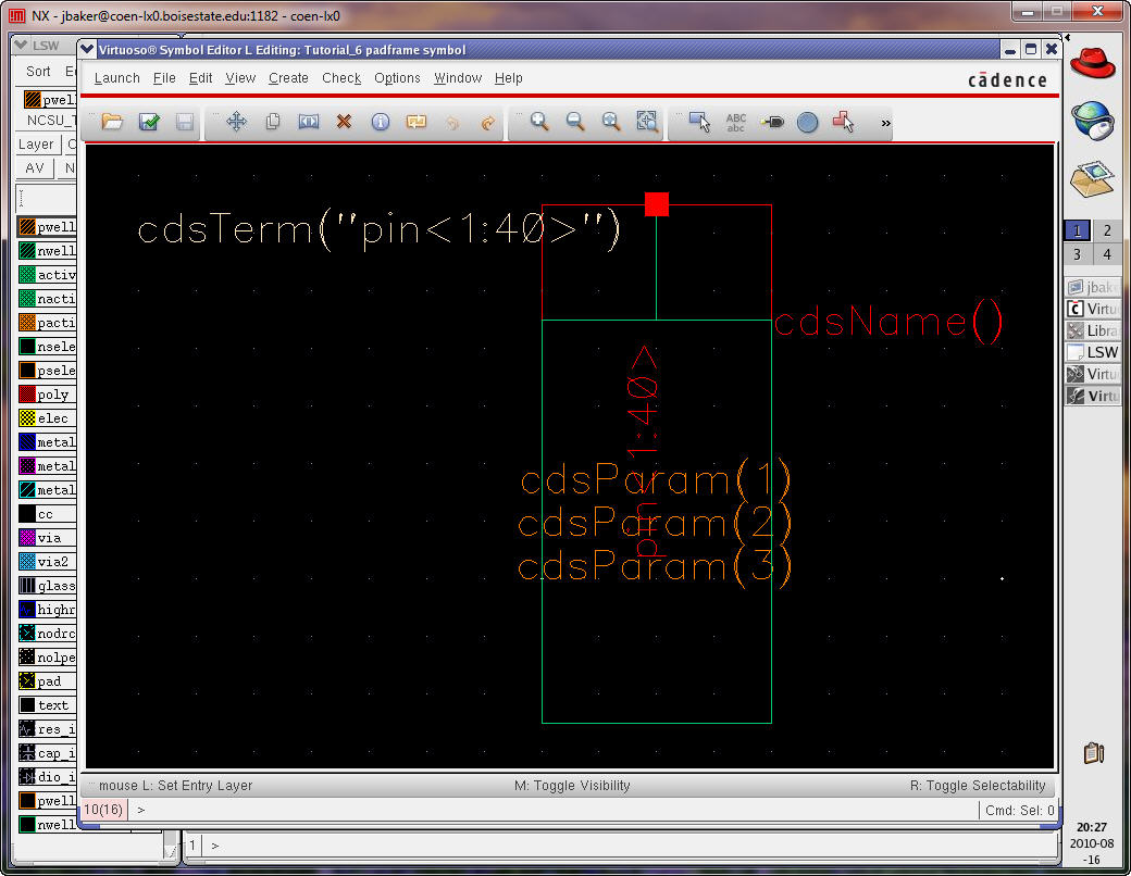
Again,
delete most items, stretch, and rotate to get the
following.
Check
and Save the symbol view.
Okay,
we are ready to create our chip layout.
Create
a schematic view of a cell called “chip” and add the cells we’ve
created in the
tutorial.
Wire
the cells up as seen (an arbitrary connection).
Note
how we’ve used pin<20> for ground and
pin<40> for power.
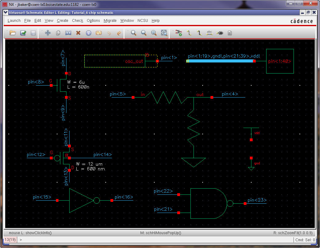
Check
and Save the chip schematic.
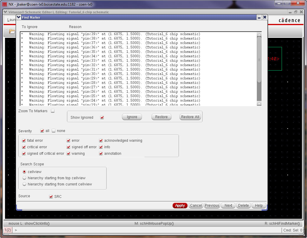
Notice
that all of the unused pins on the padframe
are
floating.
Ignore
these warnings and then Check and Save again.
We
are ready to connect the cells up to the padframe
in
the layout.
Create
of layout view of the “chip” cell.
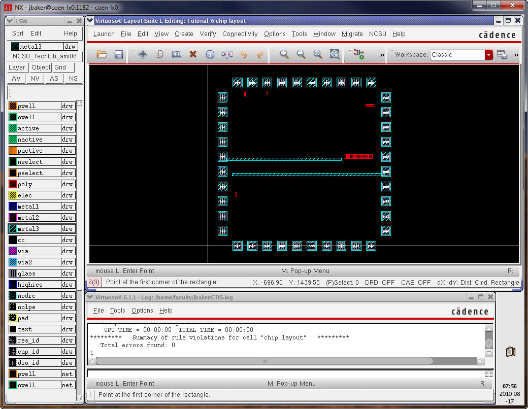
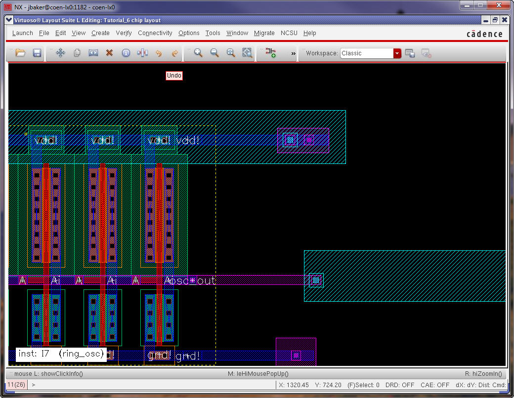
Place
the R_div,
NMOS_IV, PMOS_IV, inverter, nand2, and ring oscillator
cells near the pads that they will connect to, below.
We
can adjust the cells’ positions as needed in a moment.
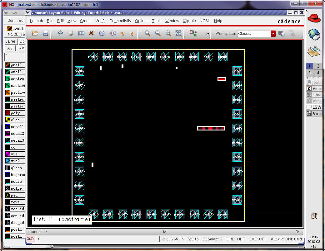
We
won’t try to make the layouts pretty but rather we’ll focus on wiring
the
circuits to the padframe
quickly.
Let’s
begin by drawing rectangles on metal3 for connections to vdd!
and gnd!
Next
let’s add rectangles on the metal layers to move towards connecting the
cells
up to the padframe.
Below
are examples zoomed in around the ring oscillator and resistive divider.
Again,
we are not trying to make a “pretty” layout (or a good one for that
matter) but
rather just connect the circuitry up.
It’s
useful to DRC the layout as you go to fix the errors that will occur.
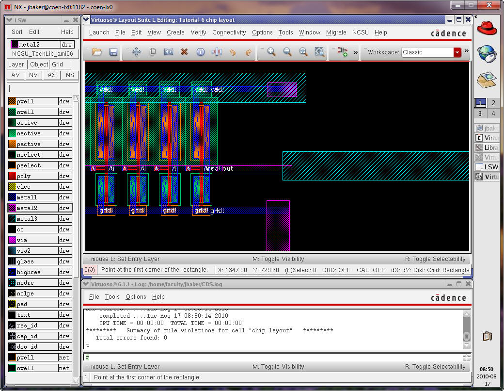
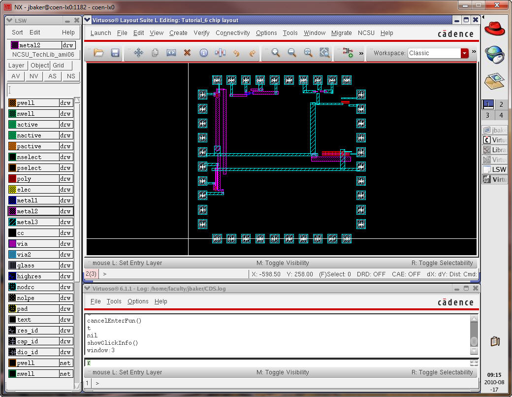
After
adding all rectangles our chip layout may look like the following.
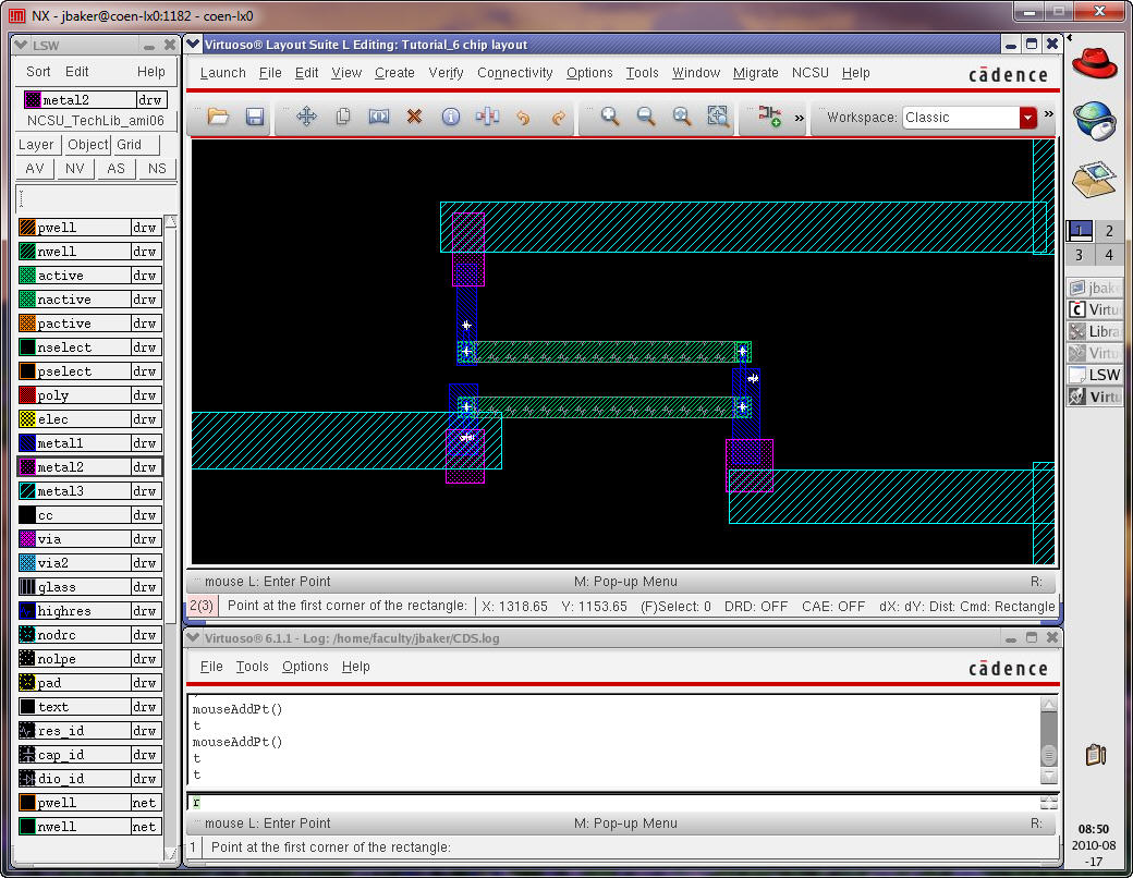
Next
let’s add vias.
Below
are examples (again, these are not examples of good layouts but rather
simply
to illustrate the operation of the tools).
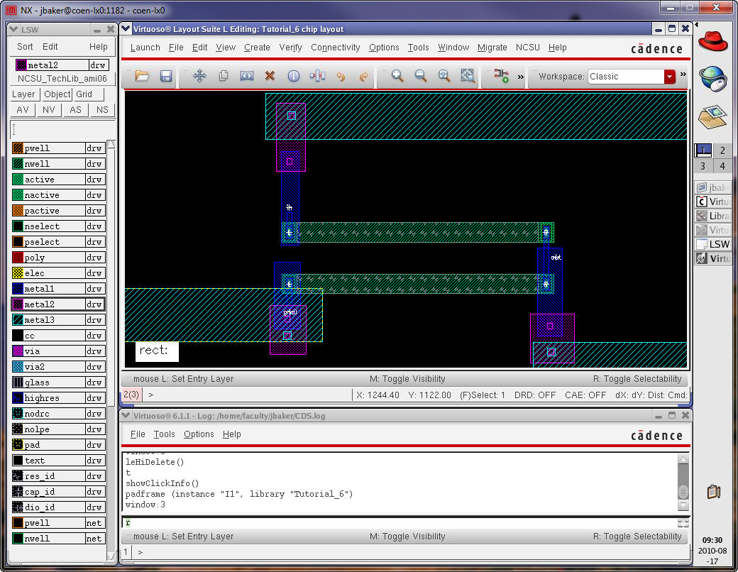
After
adding the vias let’s
extract the layout.
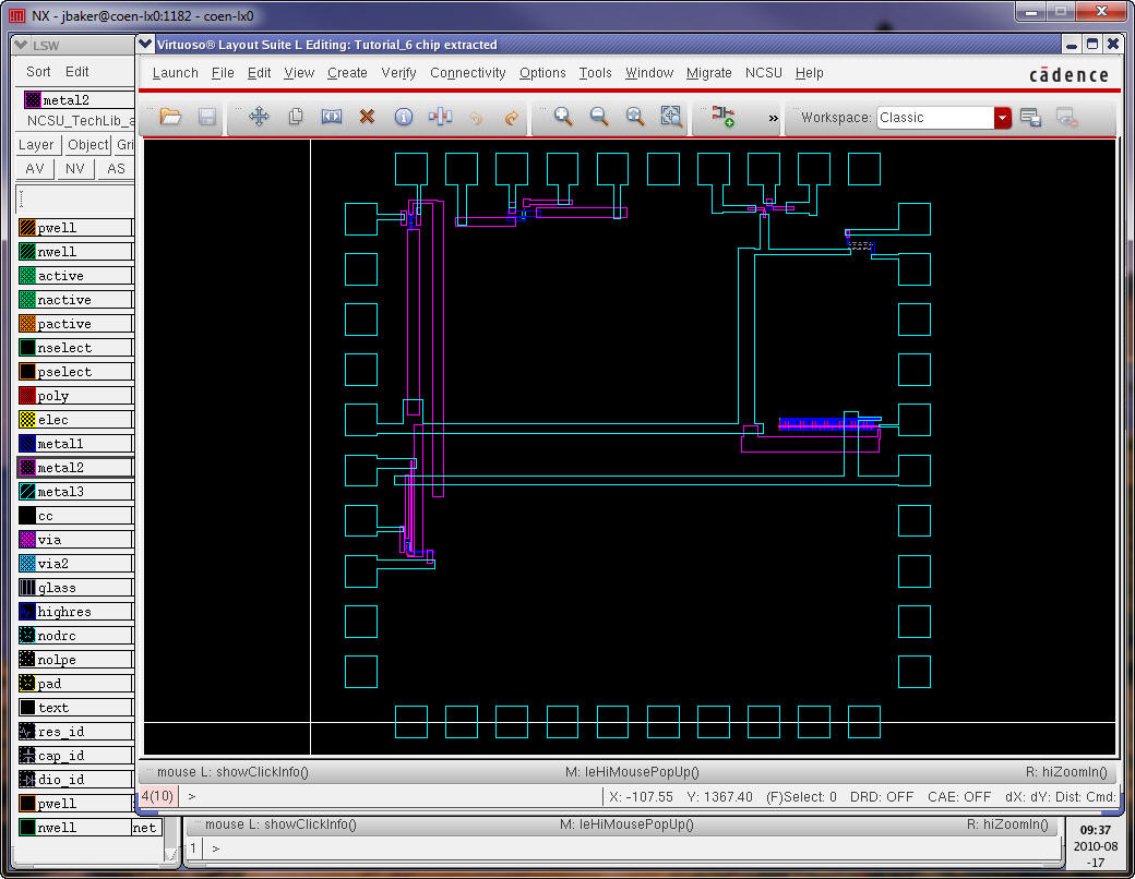
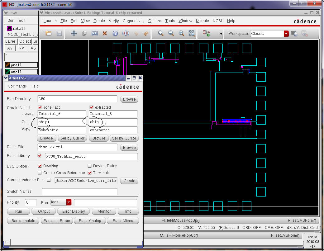
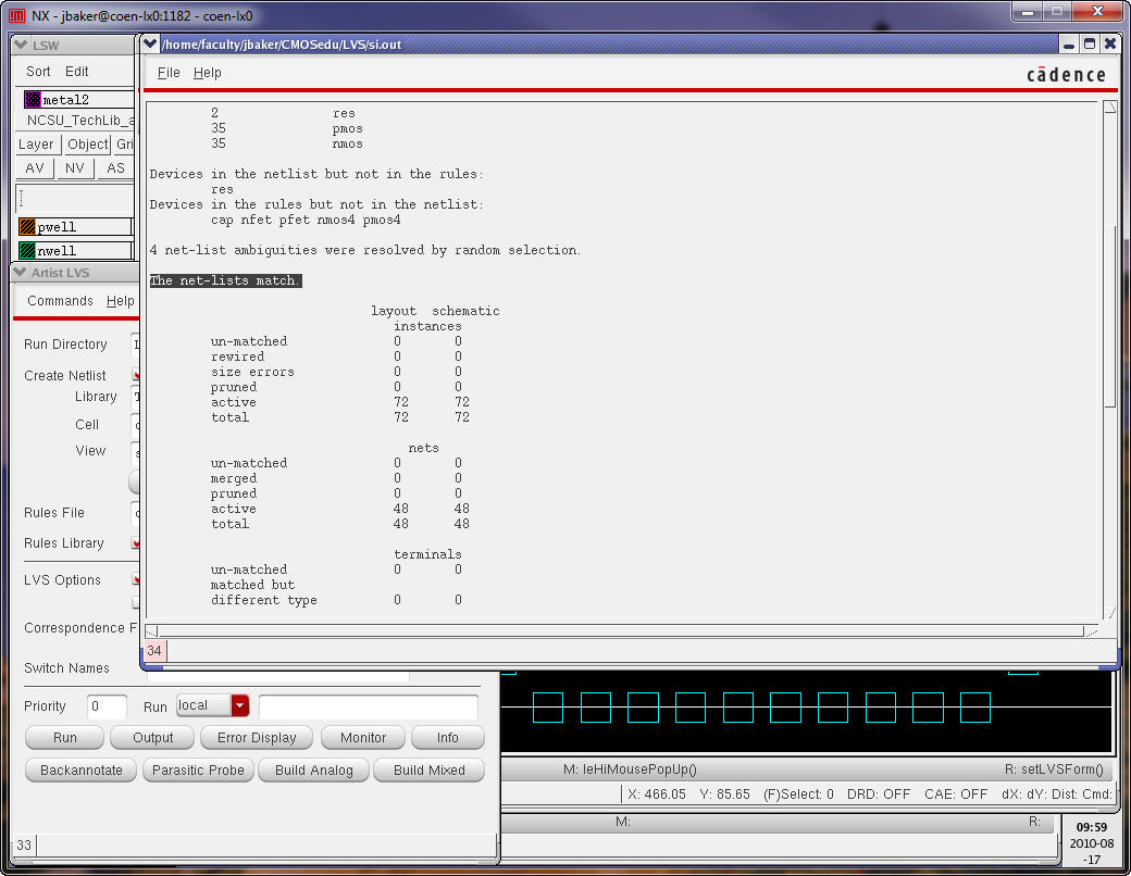
And
then perform an LVS.
This
concludes Tutorial 6.
For
your reference the Tutorial_6 directory is available in Tutorial_6.zip.