Cadence
Design System
Tutorials
from CMOSedu.com (Return)
Tutorial
4 – Design, layout, and simulation of a CMOS NAND gate
In
this tutorial
we’ll design, lay out, and simulate the operation of a NAND gate.
Instead
of using the nmos cell
in
the layout we’ll construct our nmos
device using
rectangles on various layers.
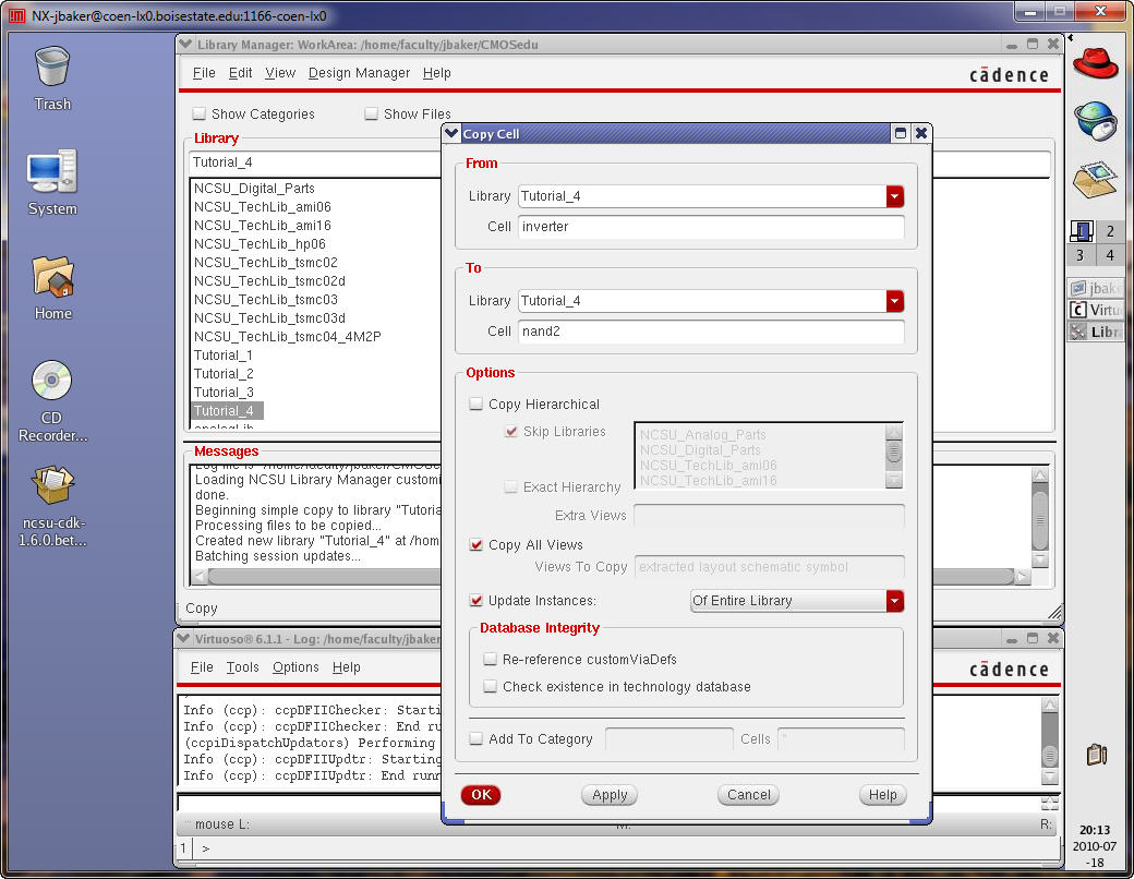
Copy
the library, Tutorial_3, into a new library called
Tutorial_4.
Ensure,
when you copy, that “update instances” is selected so
that the new library doesn’t reference cells in the other libraries.
Next
copy the inverter cell into a cell called nand2 (a
2-input NAND gate).
This
is (or may be) useful since we can copy the symbols
already in the cell to generate the circuit or layout that we want.
Finally,
copying from one cell to generate a different cell
will present other issues that should be discussed.
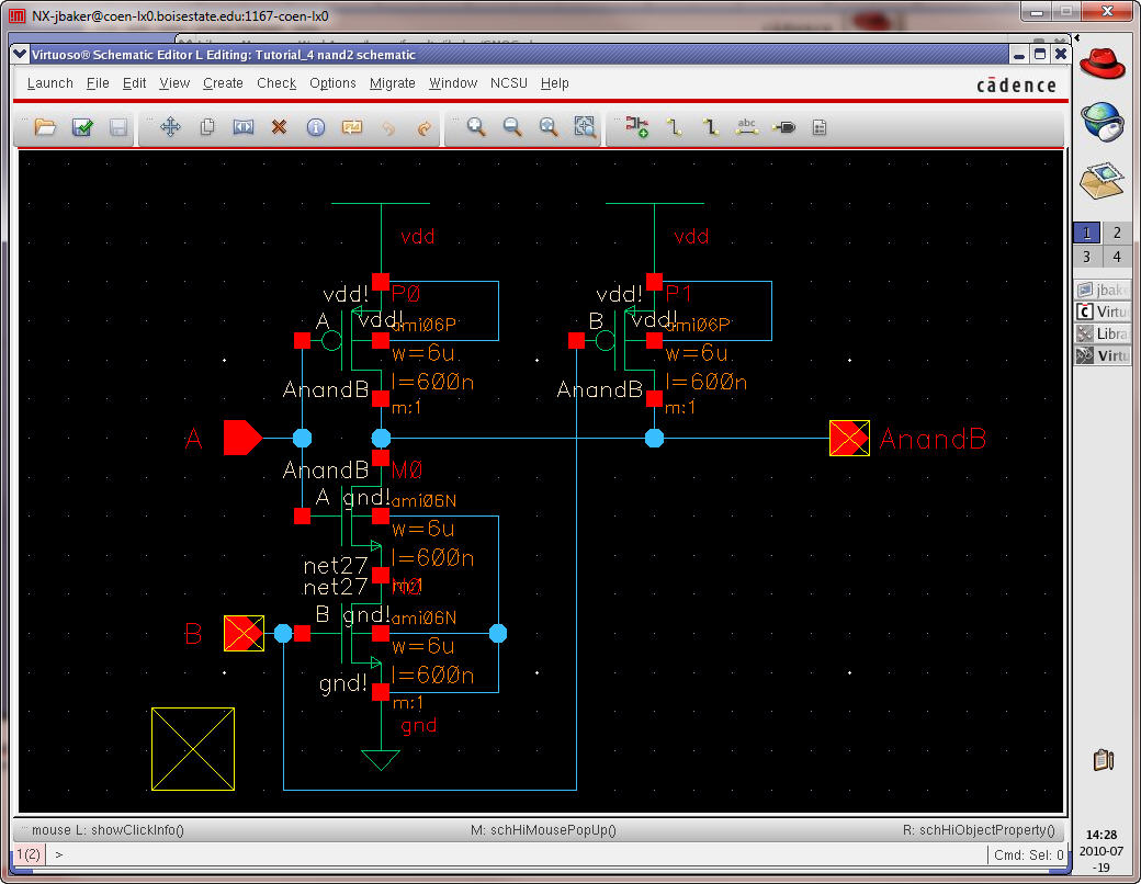
Open
the nand schematic Cell
View
and draft the schematic of a NAND gate seen below.
Note
that now the widths of the PMOS are also 6 um.
Check
and Save your design. Notice the markers (information
on what they indicate is found under the Check -> Find Markers
menu).
These
markers are the result of the symbol not matching the
schematic (remember we copied the inverter cell to make this nand cell).
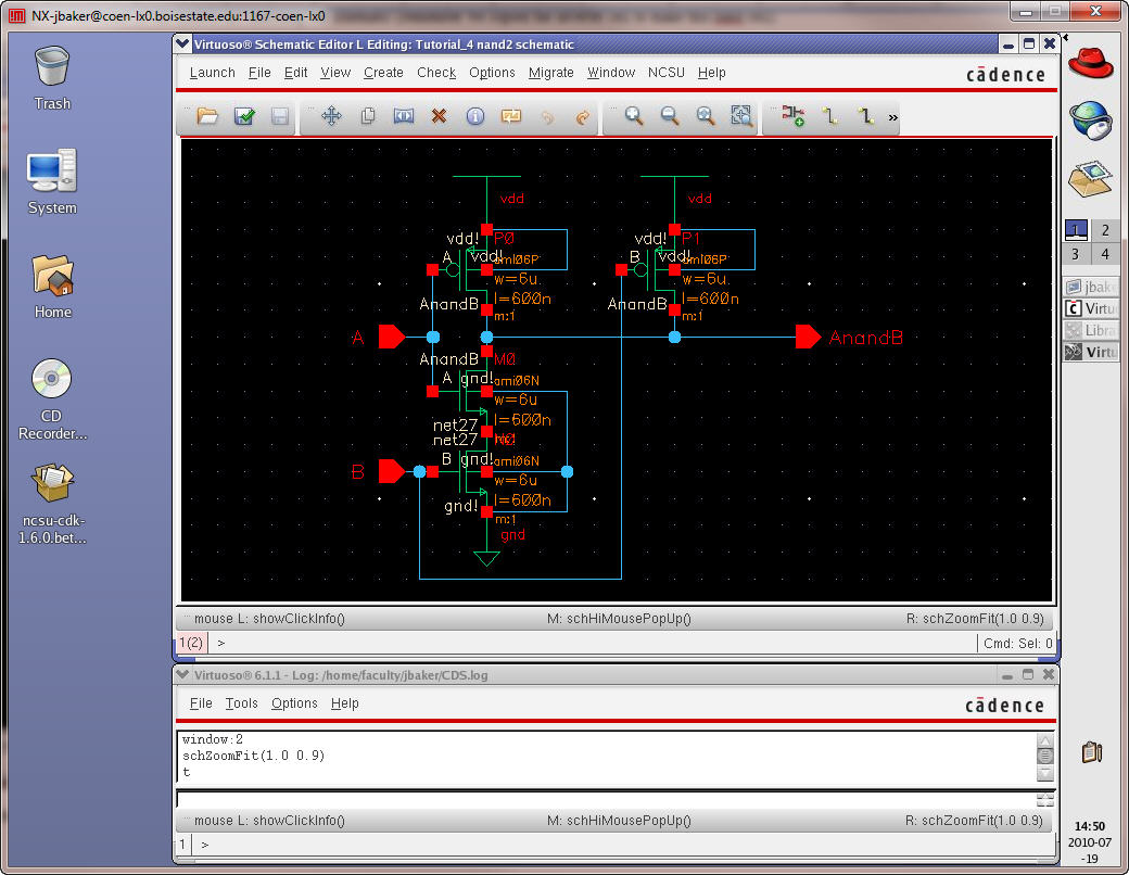
Using
the Library Manager delete the symbol view of the nand gate (which is the symbol
copied from the inverter).
Check
and Save the schematic.
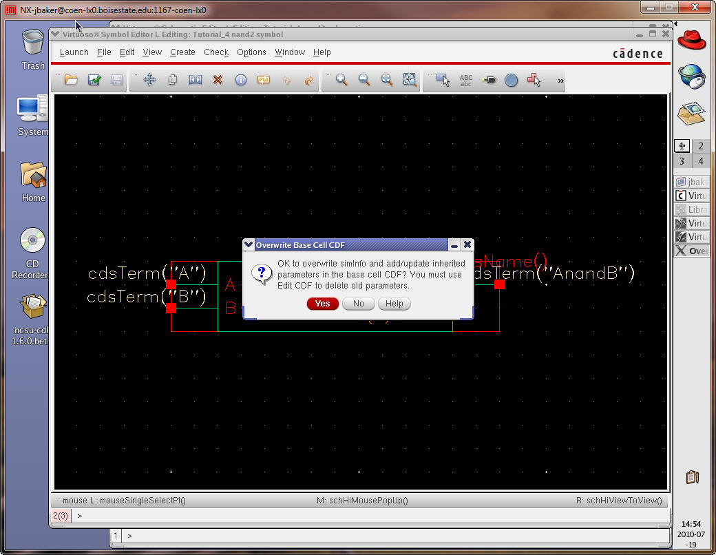
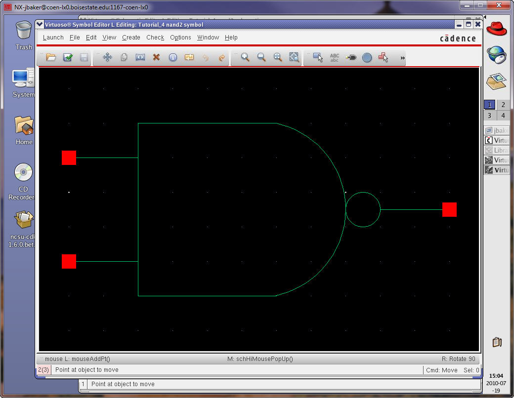
Let’s
create a symbol for this gate.
Use
Create -> Cell View -> From Cell View to create the
symbol for the NAND gate seen below.
Click
Yes to overwrite siminfo
and
add/update inherited parameters… (resulting from copying inverter to nand at the beginning of the
tutorial)
Delete
everything in the symbol except for the pins.
Draw
a NAND symbol similar to what is seen below using the
menu items found under Create.
When
finished Check and Save the symbol.
Let’s
simulate the operation of this gate.
Make
a schematic view of a cell called sim_nand2_tran and
draft the following.
Again,
as discussed in the last tutorial, if the vdd
and NAND symbols overlap the schematic won’t check and
save without errors.
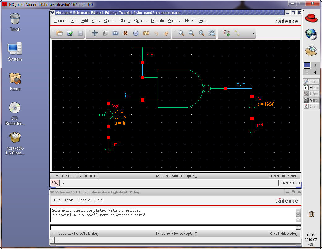
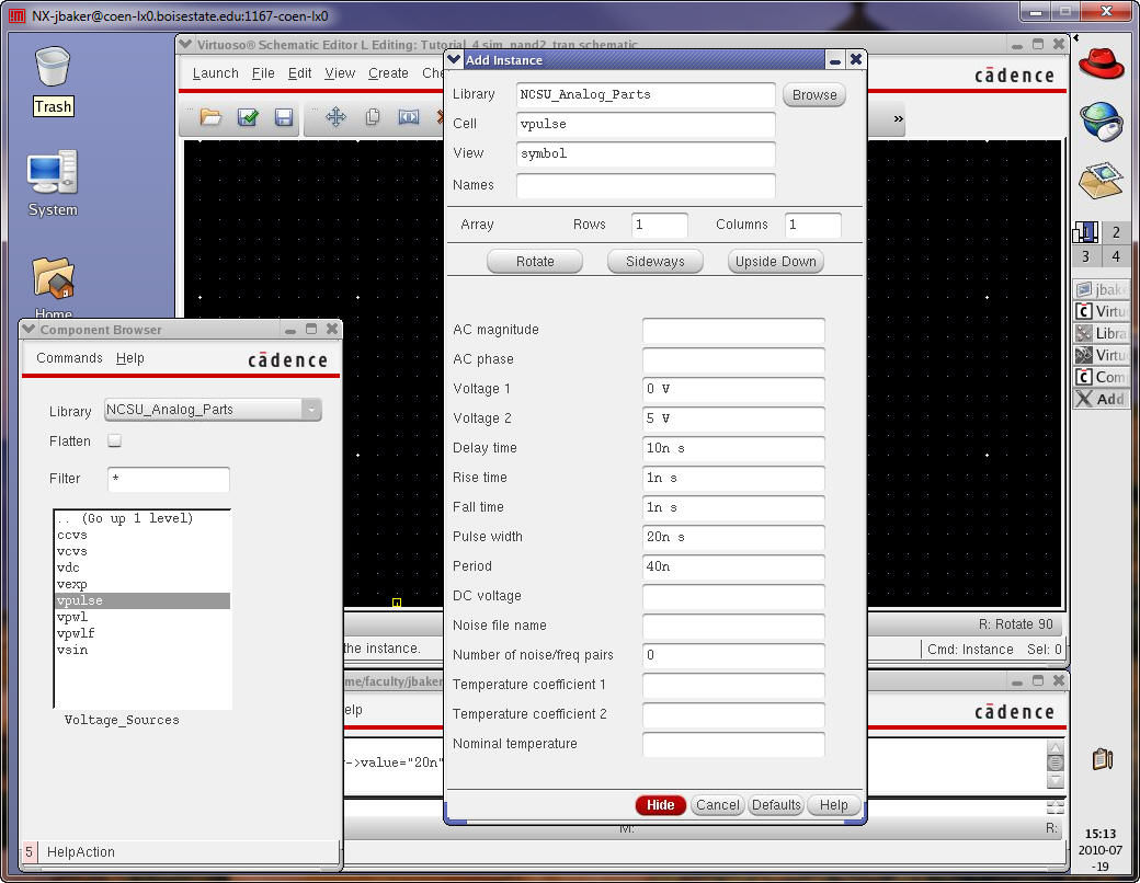
Detailed
information on setting up the pulse source seen in
this schematic is seen below.
Open
the ADE and set the models (Setup -> Model
Libraries).
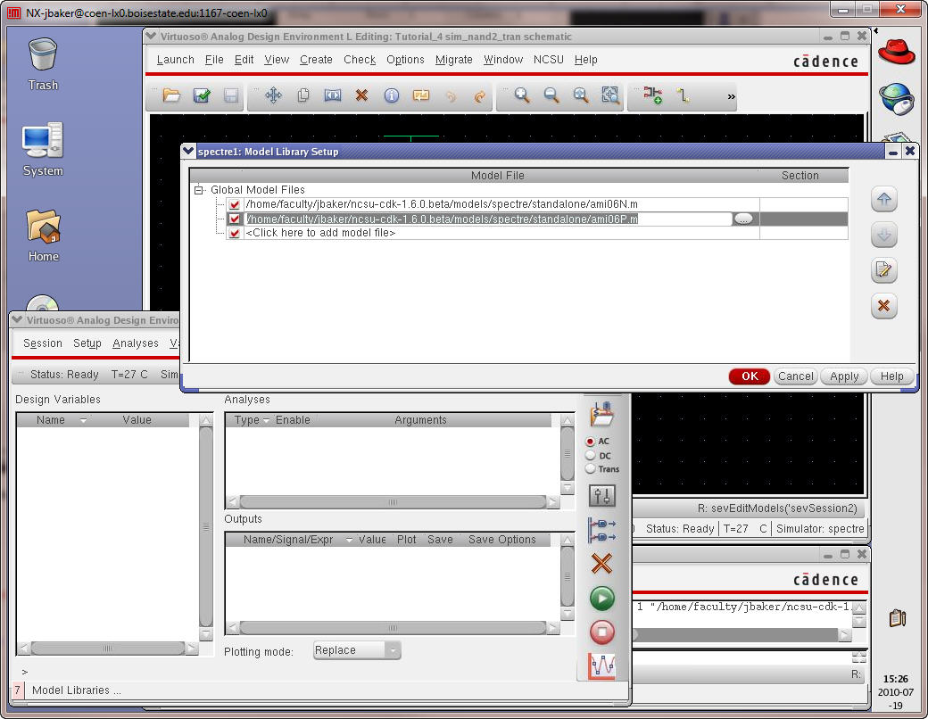
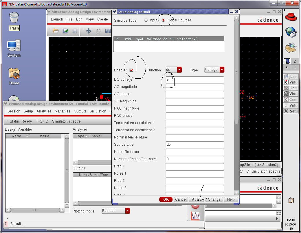
Set vdd! to 5 V via Setup -> Stimuli
Again, as discussed in Tutorial_3, if a Global stimulus
is used you can't
also place a DC source, vdc, in the schematic to generate vdd! 
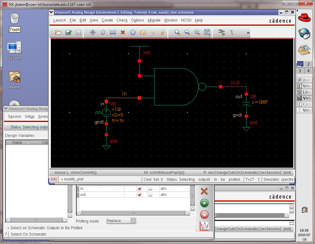
Next,
select the outputs to plot (Outputs -> To Be Plotted
-> Select On Schematic).
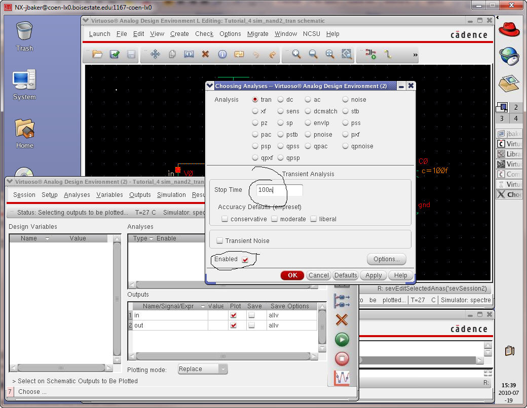
Finally,
set the Analysis to a transient then Save the
State.
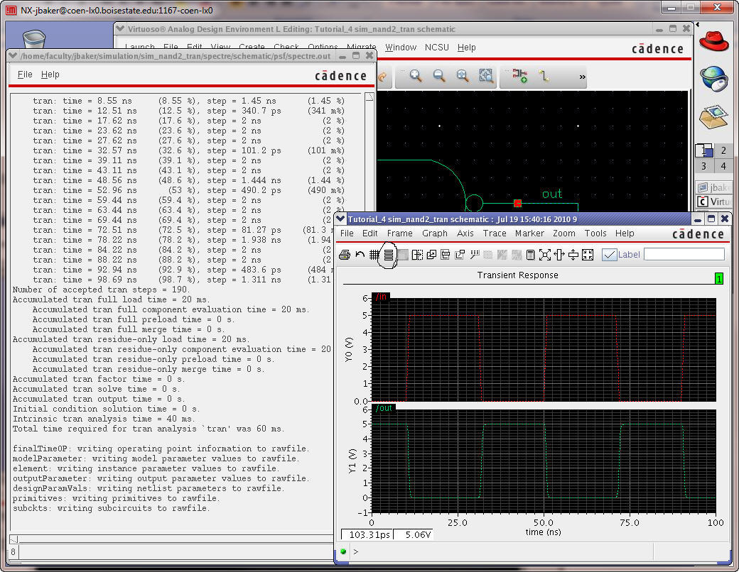
After
Saving the state (Cellview)
Netlisting and Running
gives the following (using the Strip
Chart Mode circled below)
Close,
and save, all open Cell Views.
Next,
use the Library Manager to open the nand
layout cell view (which shows the inverter, since we copied it at the
beginning
of the tutorial).
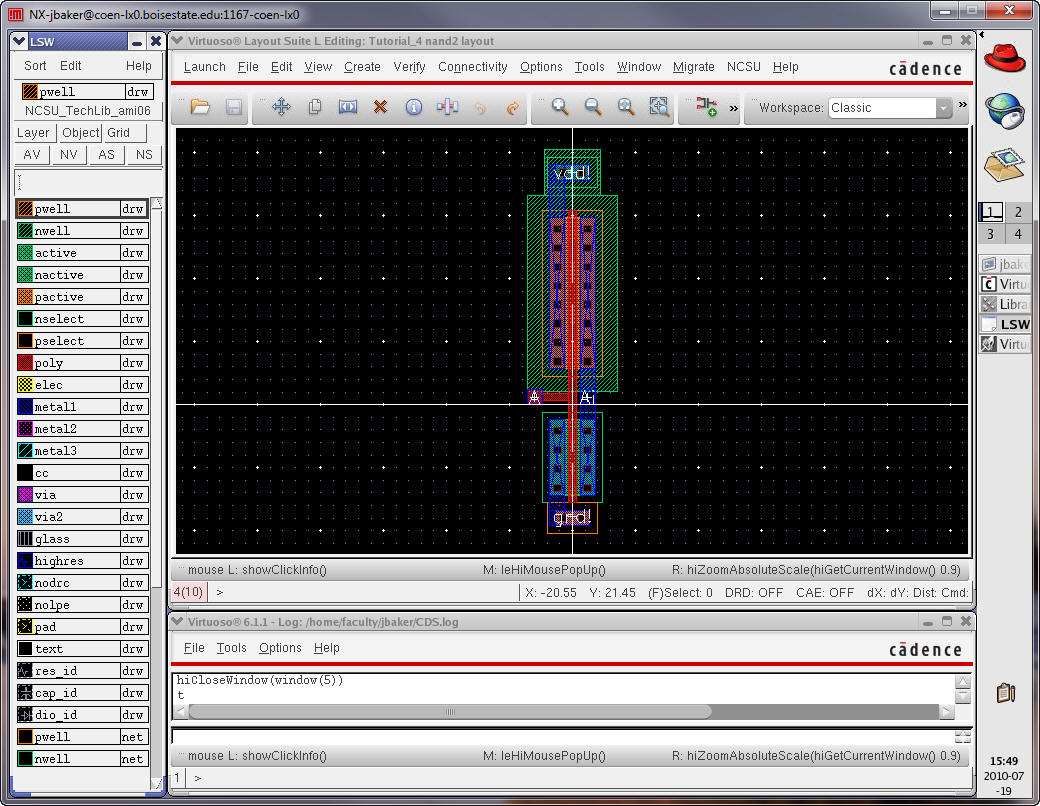
Delete
the metal1 and Ai pin connecting the drains of the
MOSFETs.
Delete
the metal1 connecting the source to the ptap
then delete the gnd!
pin.
Move
the ptap to the left
side of
the layout.
DRC
the layout (which should look like something like what is
seen below) to ensure no errors.
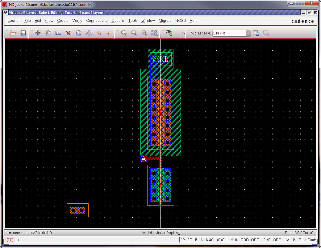
Next
delete the metal1 from the ntap
to the source of the PMOS and delete the vdd!
pin
Copy
the pmos cell as seen
below.
Move
the right pmos until it
overlaps the left pmos
as seen below.
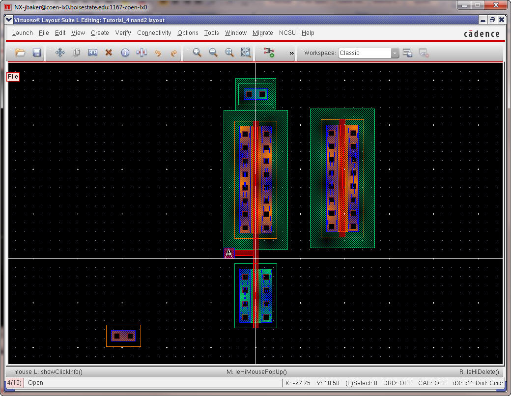
Change
the ntap cell so that
it has
5 columns of contacts.
DRC
the layout.
Next
change the ptap cell so
that
it has 5 columns of contacts.
Move
the ptap cell so that
it is
under the nmos cell.
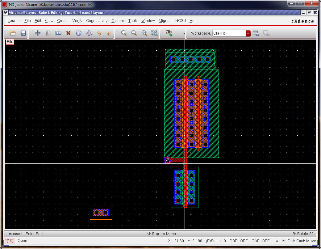
Zoom
in around the bottom of the layout.
Now
we can copy a second nmos
and
overlap it with the first, like we did above for the PMOS (do this now).
Let’s
also move the m1_poly and A pin over adjacent to the
vertical poly and add a poly rectangle, m1_poly, and B pin (input) for
the
added PMOS.
Ensure
that pin names are showing, the pins are added on
metal1. Let’s go ahead and add pins (inputOutput)
for
vdd! and gnd! while we are
at it.
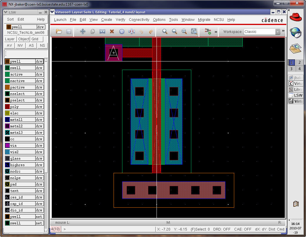
The
result is seen below.
We
don’t need the metal in between the two MOSFETs.
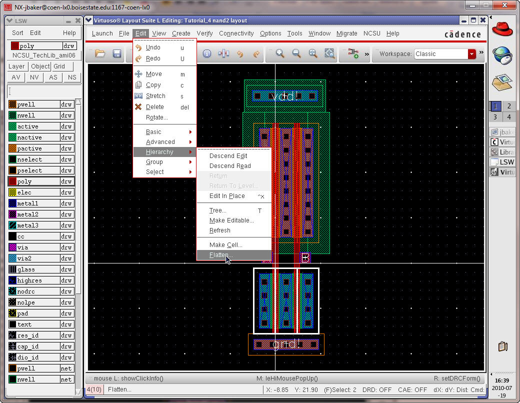
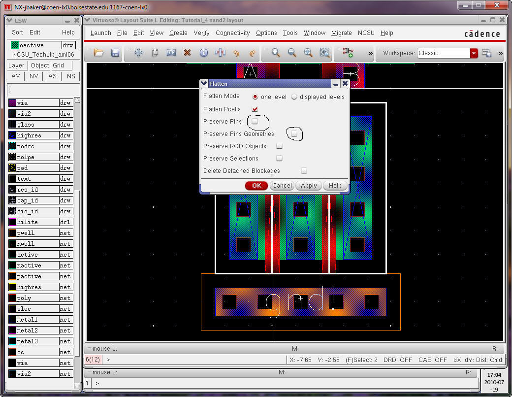
Select
both MOSFETs then flatten them (makes it so the nmos
cells are no longer cells but rather rectangles in the
layout).
De-select
Preserve Pins Geometries.
This
ensures that the geometric information of flattened pins
is not preserved.
We
don’t want pins or the pin information in our layout. We
want the flattened cells, the rectangles, placed as if we drew them.
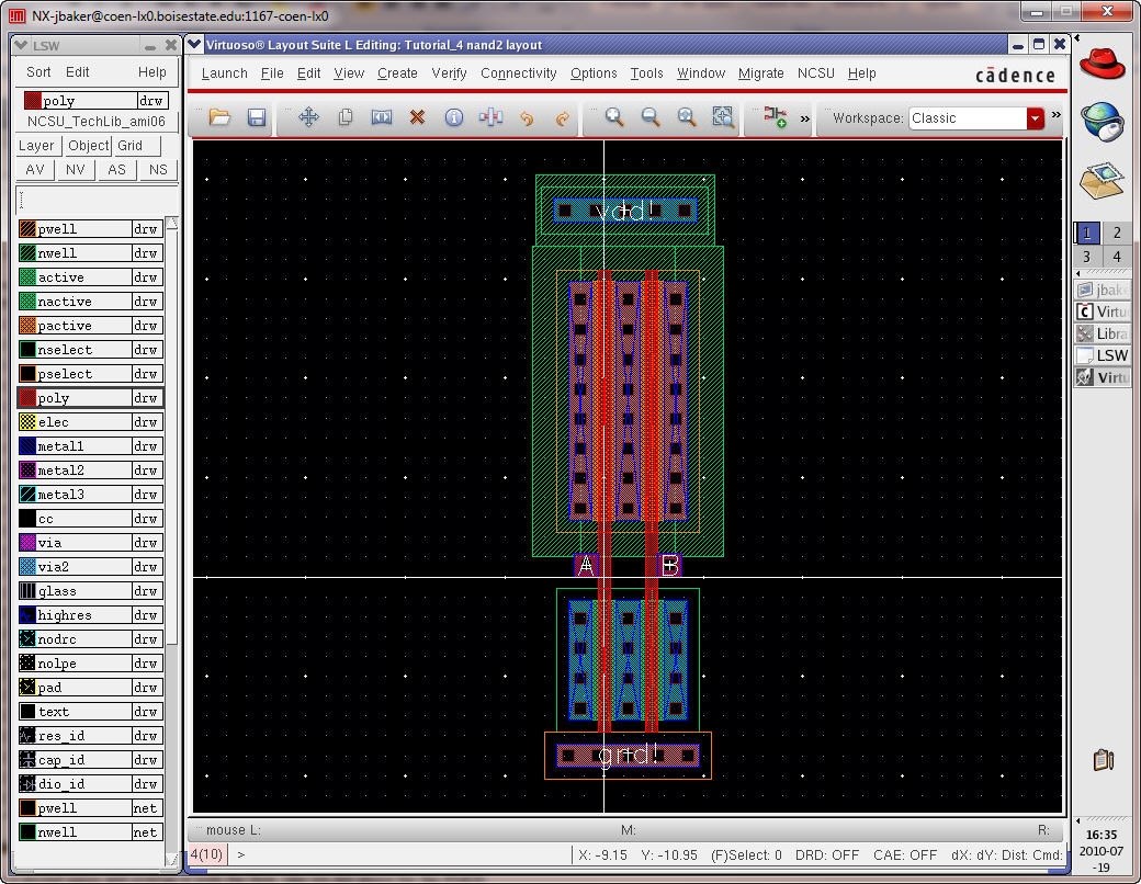
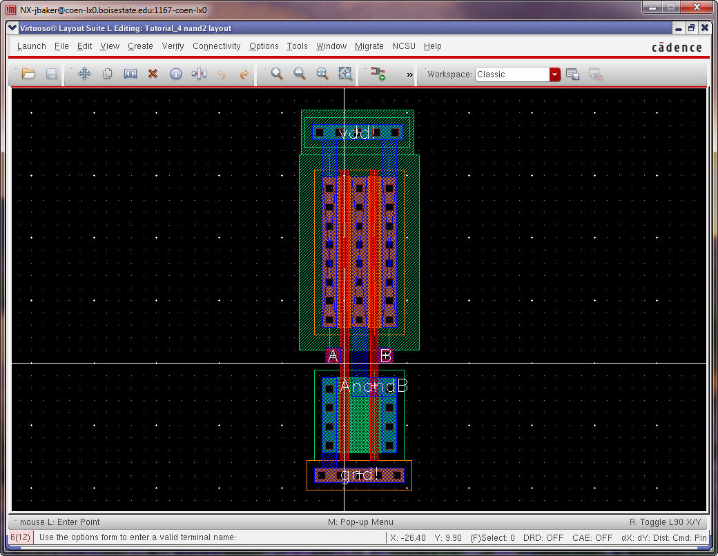
Delete
the metal1 and contacts between the two nmos.
Add
metal1 to gnd!, vdd! (two places), and connect
the drains of the two pmos
to the drain of the nmos.
Finally,
add a pin, AnandB
(output
direction) as seen below for the final layout.
DRC
the layout.
Extract
the layout and open the extracted view with the
Library Manager.
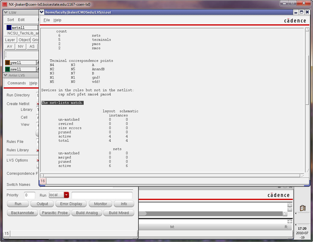
Run
the LVS.
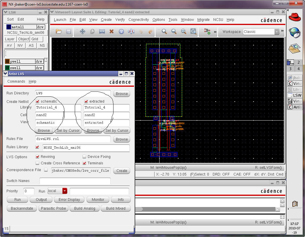
To
show the layout and schematic match.
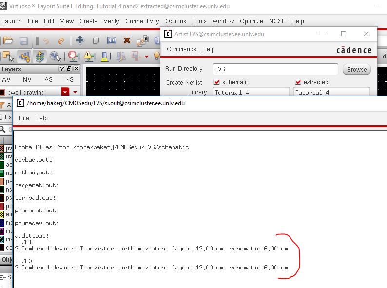
However! Notice that the size of the PMOS devices in the schematic differ from the size of the PMOS devices in the layout.
Let's fix this. Close the Artist LVS tool (important).
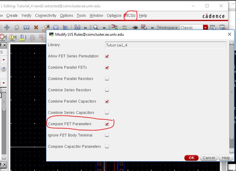
On the top menu in the Extracted or Layout views select NCSU -> Modify LVS Rules... as seen below.
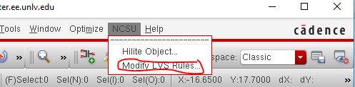
Next select Compare FET Parameters as seen below.
Re-run the LVS and we get the following error (after clicking on the Output button on the Artist LVS
window) showing the size of the PMOS devices in the schematic and layout don't match.
Save
and close everything. This concludes Tutorial 4.
For
your reference the Tutorial_4 directory is available in Tutorial_4.zip.