Cadence
Design System
Tutorials
from CMOSedu.com (Return)
Tutorial
5 – Design, layout, and simulation of a ring oscillator
In
this tutorial we’ll design, lay out,
and
simulate the operation
of a ring oscillator.
At
this point we should be getting comfortable with the tools.
One
of the goals of this tutorial is to teach how to use arrays and buses
Copy
the library, Tutorial_4, into a new library called Tutorial_5.
Ensure,
when you copy, that “update instances” is selected so that the new
library
doesn’t reference cells in the other libraries.
As
always, put the new library in $HOME/CMOSedu
Create
a new schematic cell view called ring_osc.
In
this cell view place the inverter symbol that was created in tutorial 3.
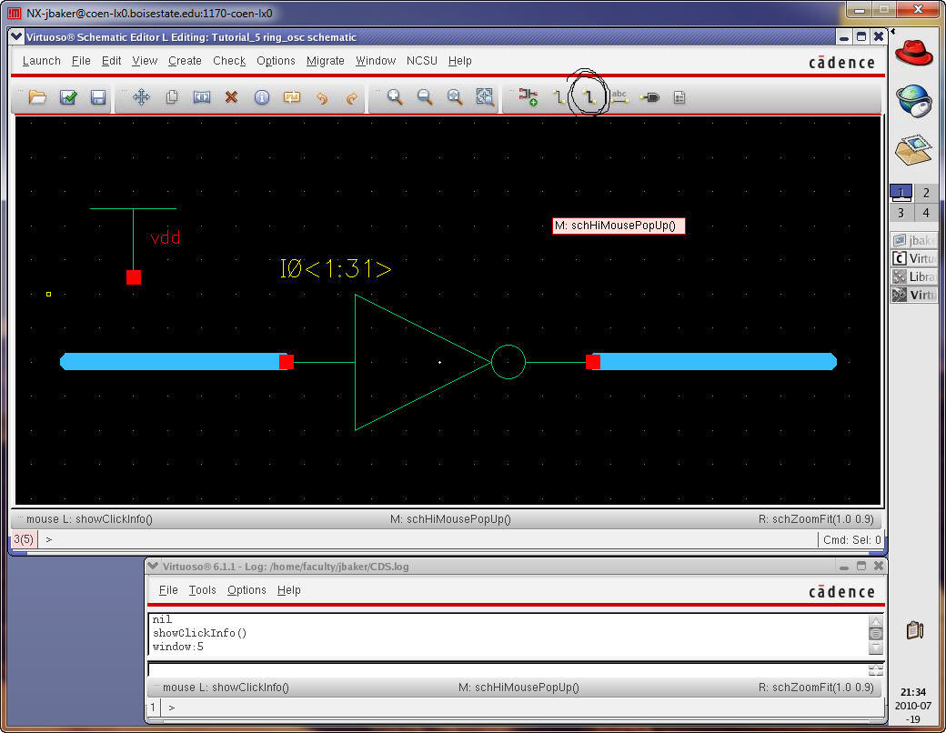
Also
place the vdd supply
net symbol, see below.
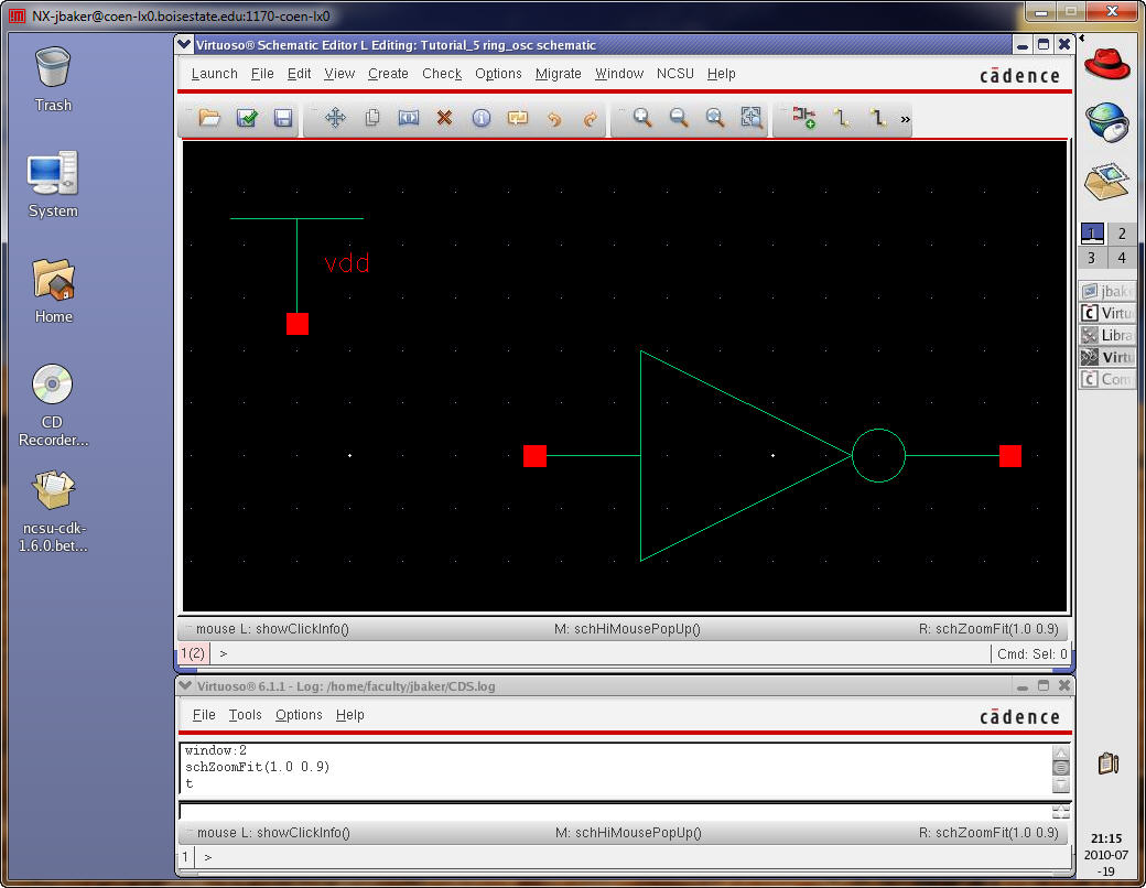
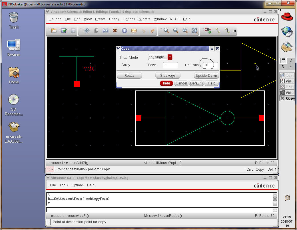
Next
press c (for copy) and the inverter
(to copy the inverter).
Before placing the
copy of the inverter press F3
(special options).
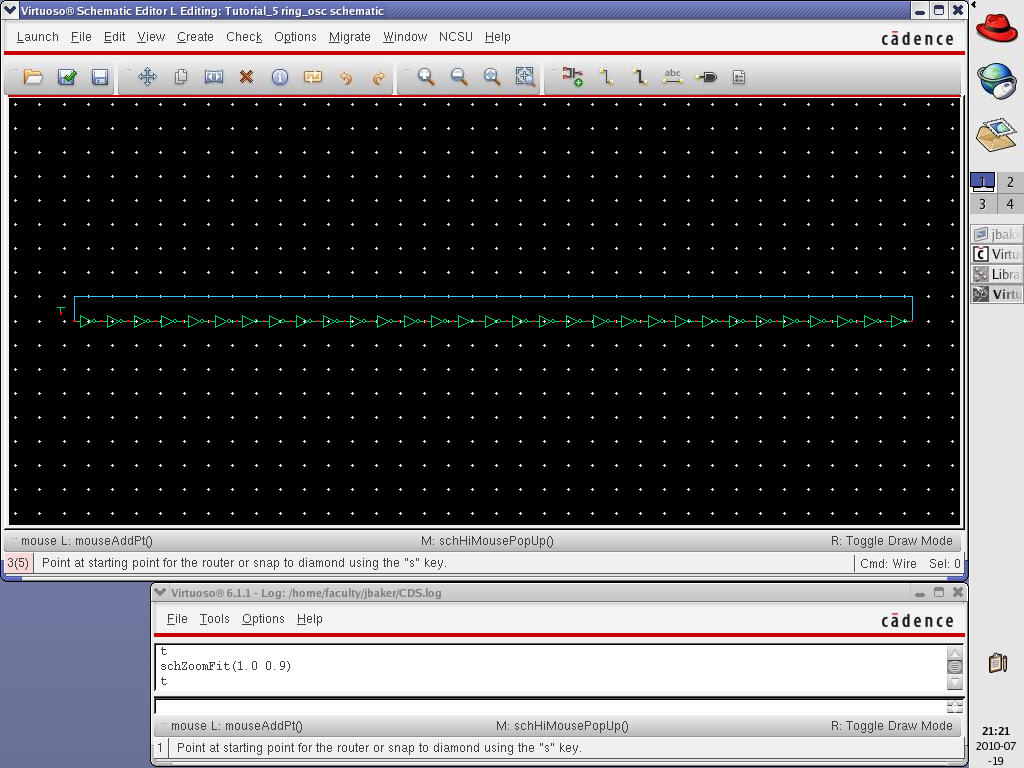
We’ll make a 31
stage ring oscillator so select 30 columns as seen below (to add 30
inverters
to the existing one).
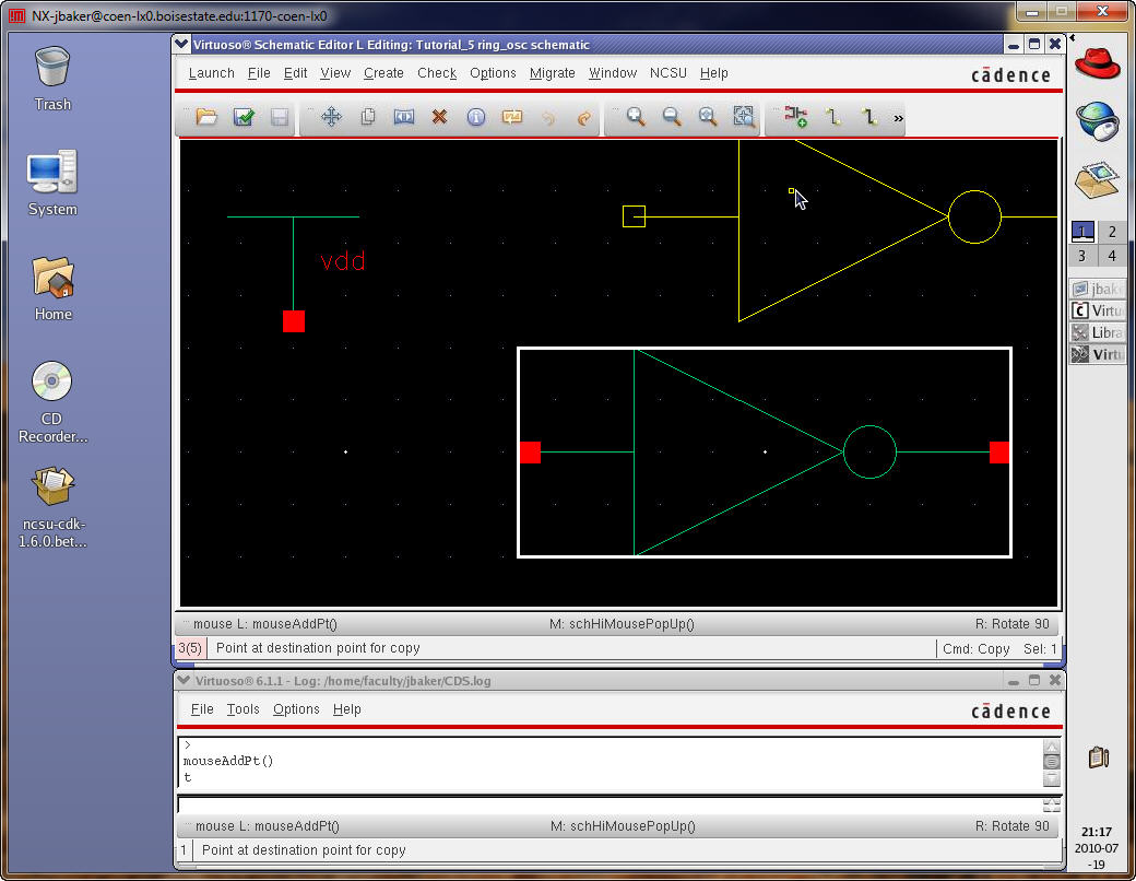
Instantiate the
(first copied) inverter on the output of the existing inverter.
Repeat for the
second copied inverter to get the following.
Note that if we
wanted a wire between the inverters we could have added the wire on the
output
of the first inverter and then copy both the inverter and wire.
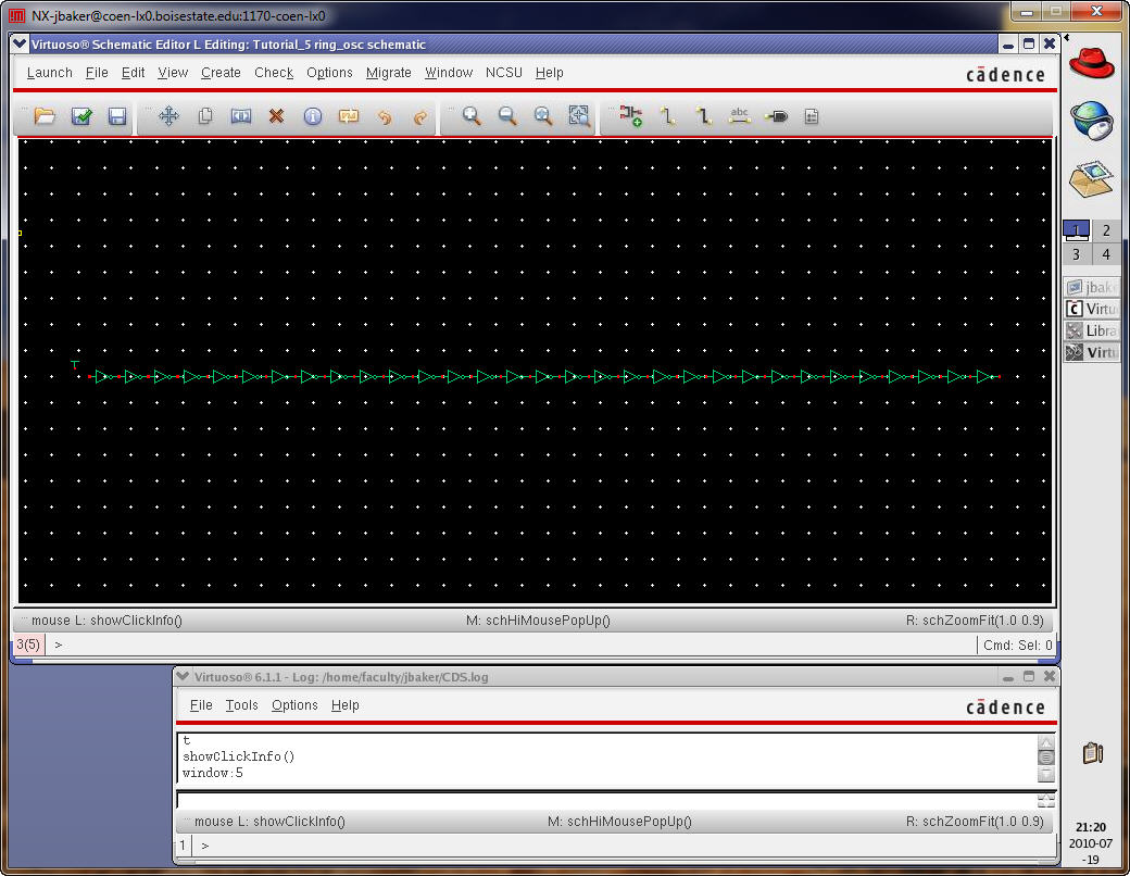
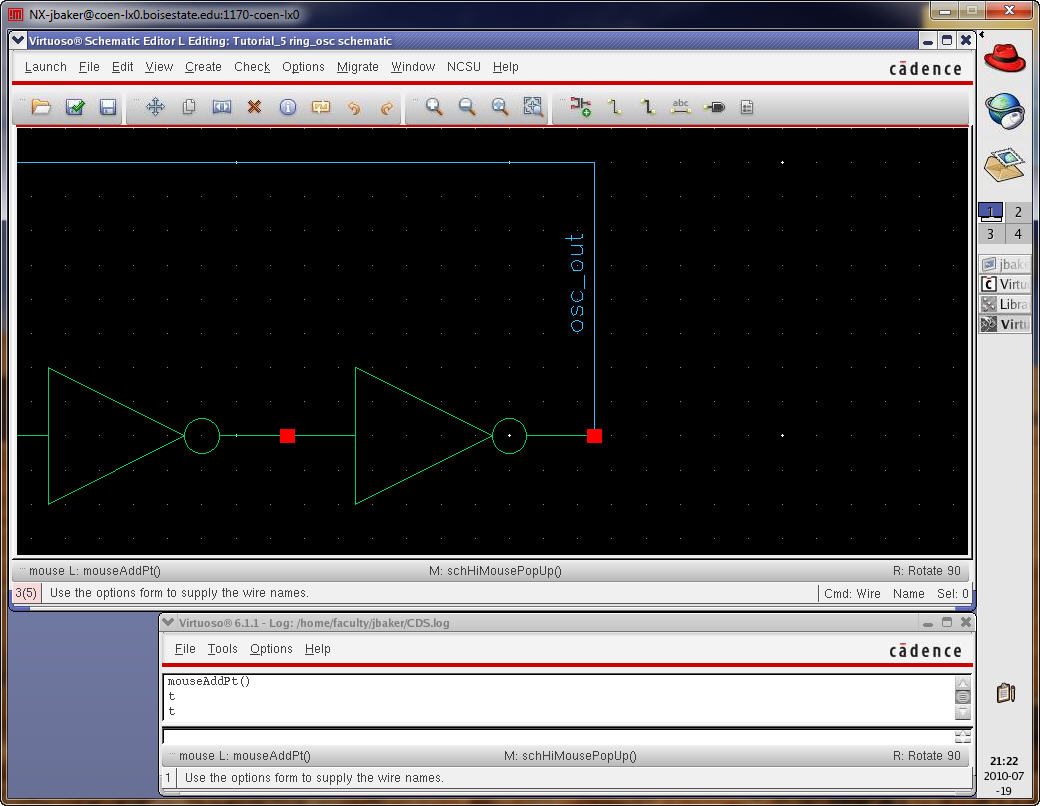
Add a wire
connecting the output of the last inverter to the input of the first
inverter.
Label the wire osc_out as seen below.
Check and Save the
schematic.
Now start the ADE.
Set the MOSFET
models (Setup -> Model Libraries).
Set the vdd! to 5 V (Setup ->
Stimuli), or add a vdc (but not
both as discussed in Tutorial_3), 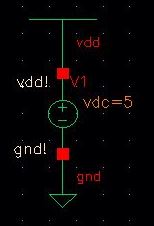 .
.
Select the outputs
to plot (select osc_out)
Set the analysis
to a transient with a length of 200 ns.
If doing any of
these things is a challenge review tutorials 3 or 4.
Save the State (Cellview) and “Netlist and Run”
the simulation.
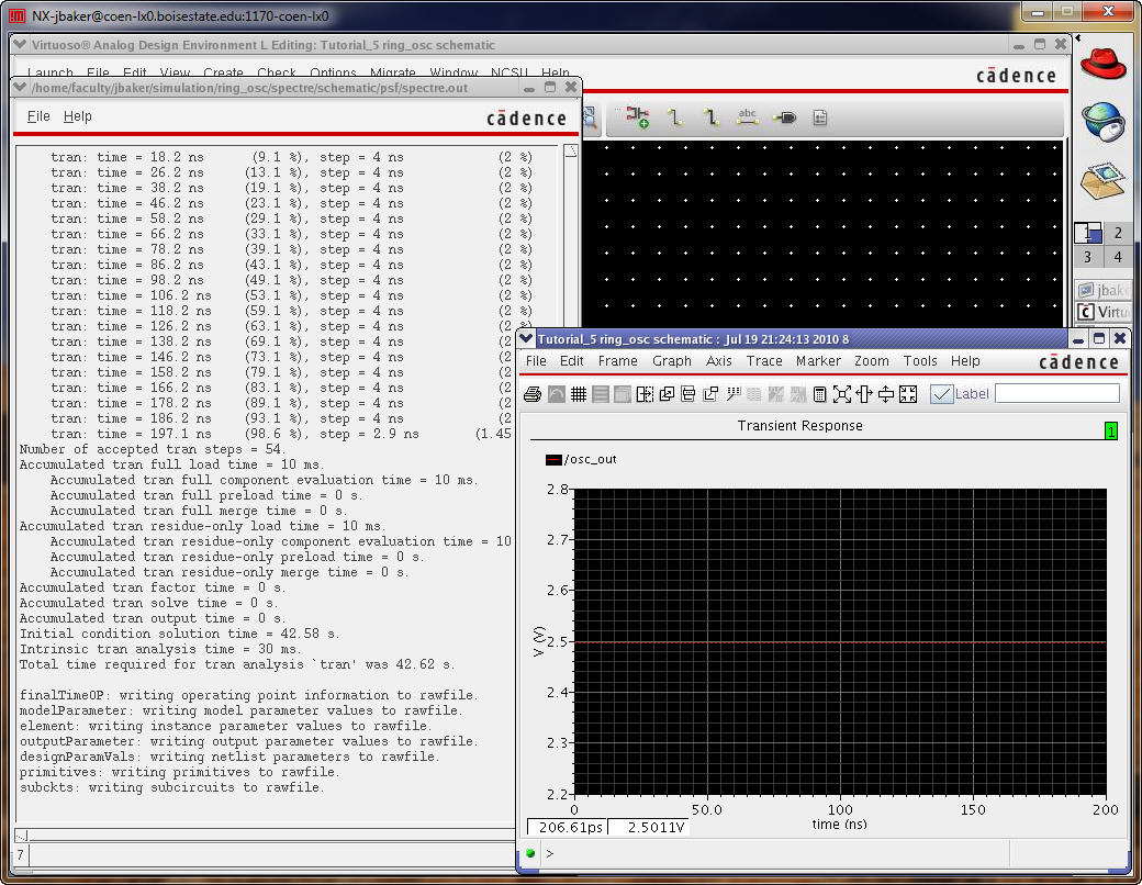
The output is
steady at 2.5V!
In a real circuit
noise would kick-start the oscillations.
Let’s do this in
the simulation by adding an initial condition.
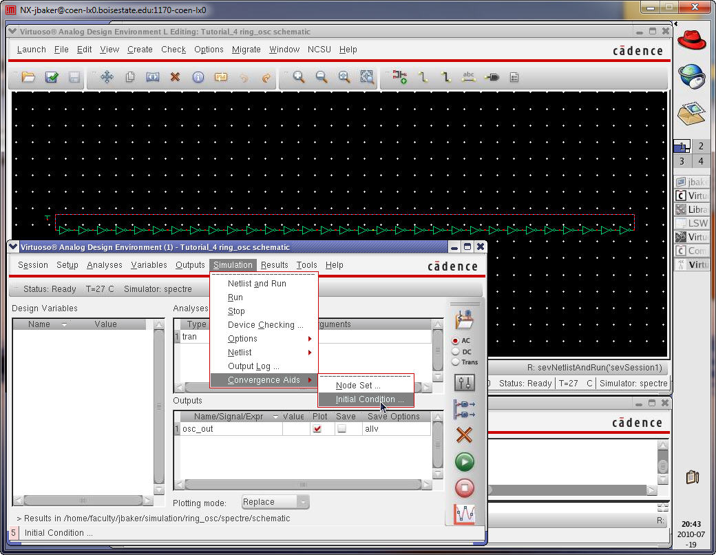
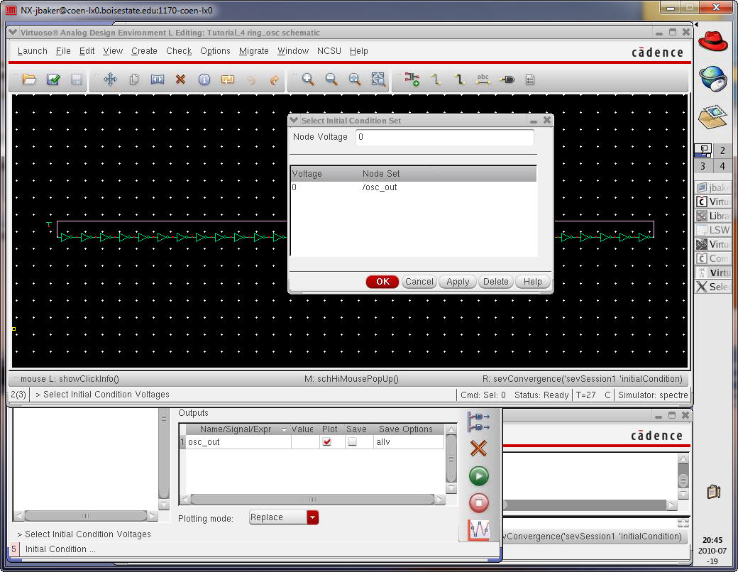
Select a node
voltage of 0 and click on the wire labeled osc_out
results
in what is seen below (you may have to access the menu again to view
this
condition).
Save the state of
the simulation.
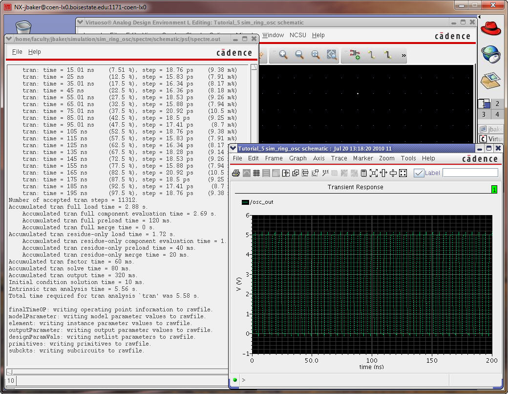
After saving the
state and simulating again we get
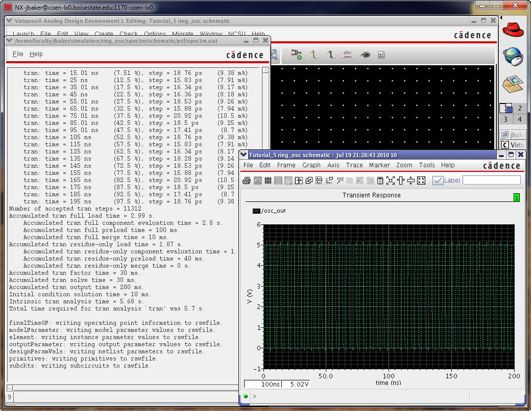
which is what we
expect a ring oscillator to do ;-)
Save the state and
close the ADE.
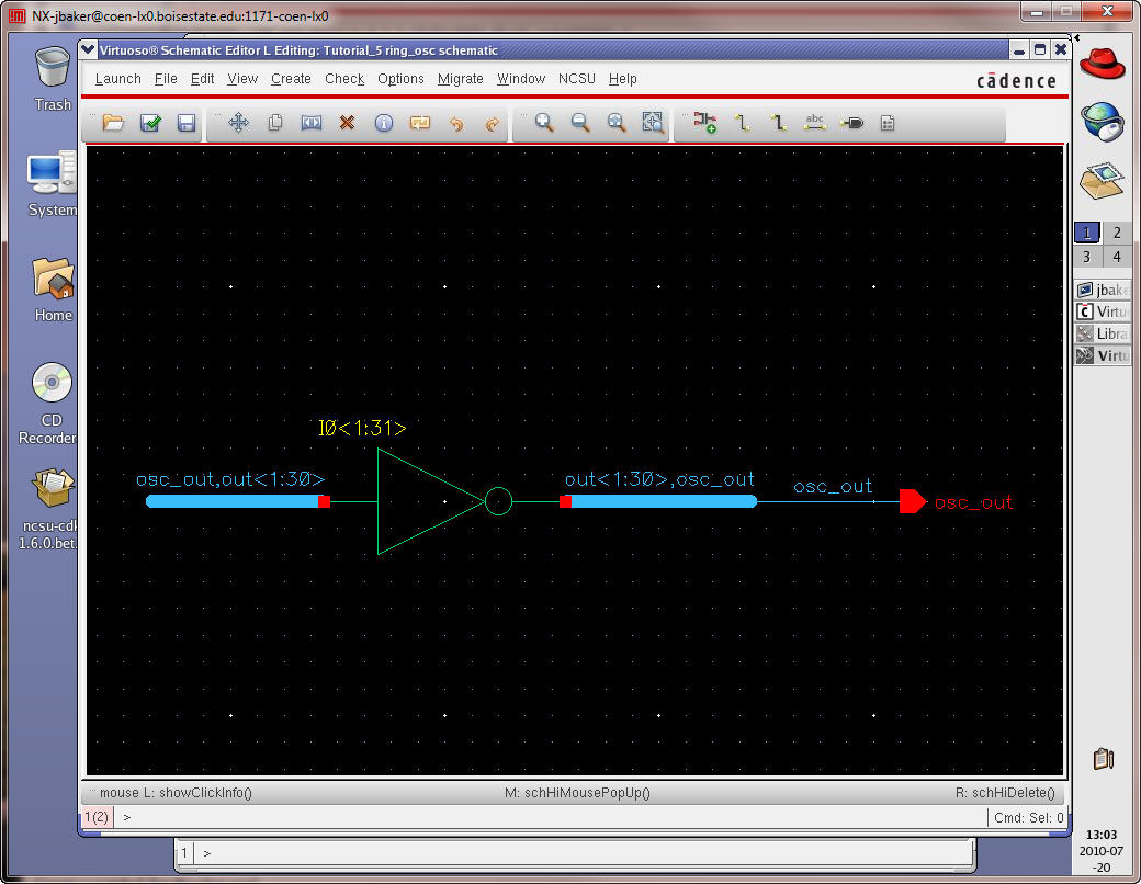
Let’s
make the schematic more pleasant to look at.
Delete
all of the inverters and the wires except for the
first inverter.
Change
the inverters name from I0 to I0<1:31> (an array
of 31) and display the name (value).
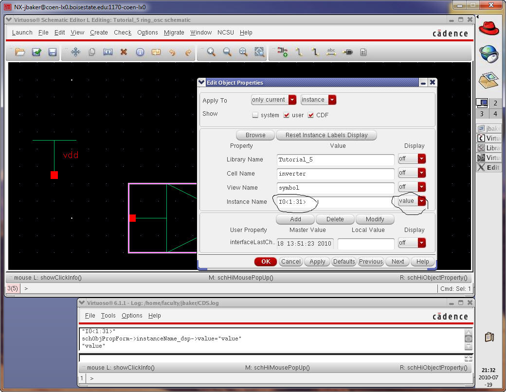
Now
use the wide wire (W)
to connect to the input and output of the symbol.
Use
the wire label (l)
to add names as seen below.
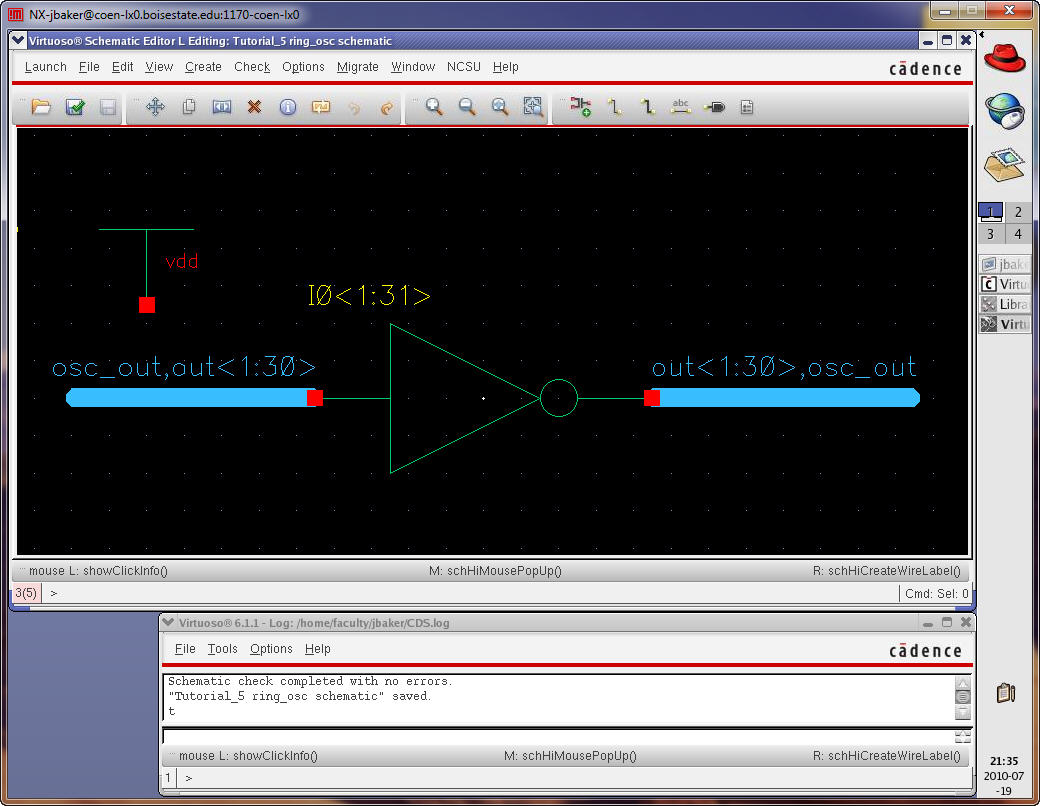
The
input of I0<1> is osc_out
and its output is out<1>
The
input of I0<2> is out<1> and its output is
out<2>
The
input of I0<3> is out<2> and its output is
out<3>
The
input of I0<31> is out<30> and its output
is osc_out
The
schematic is exactly the same as the one we drew earlier
but clearly nicer to look at (more concise).
Re-simulating
this ring oscillator gives the exact same
results as seen above.
Save
and close all cell views.
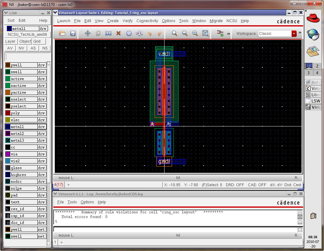
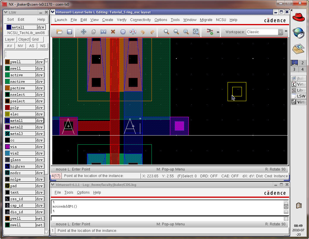
Create
layout view for the ring oscillator and place two
inverter layouts in the cell next to each other.
DRC
the layout.
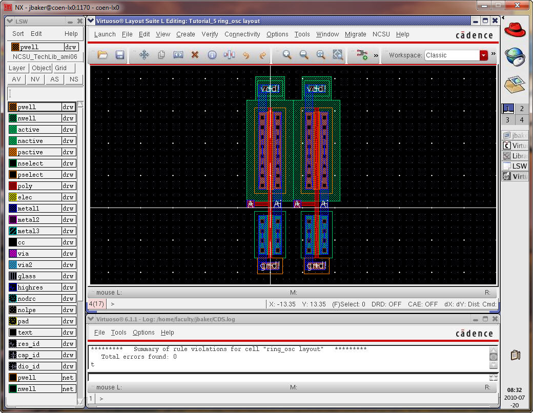
Add
rectangles of metal between vdd!,
Ai of the first inverter and A of the second inverter, and gnd!
as seen below (where e was pressed
and
the stop display level was set to 0 to hide the layout of
the inverter).
DRC
the layout.
Set
the stop display level back to 10 and delete the right
inverter.
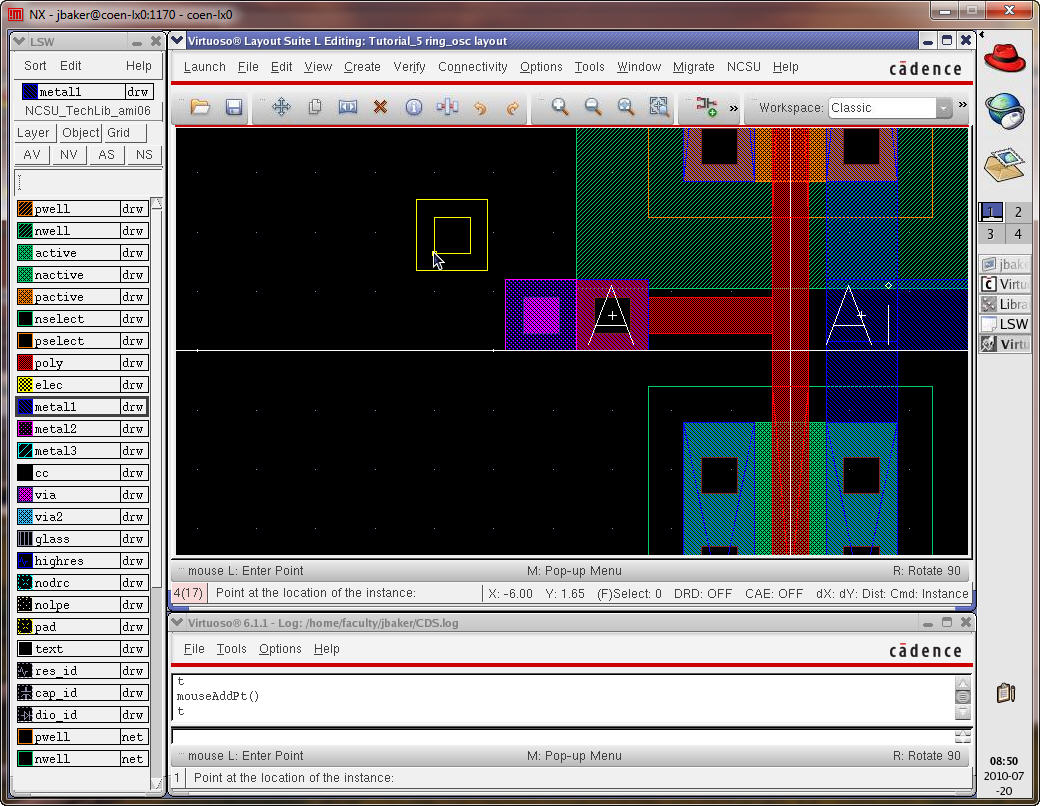
Next
select press c
(to copy) and select the entire layout.
Press
F3, special options, and set the number of columns to
30 (as was done above).
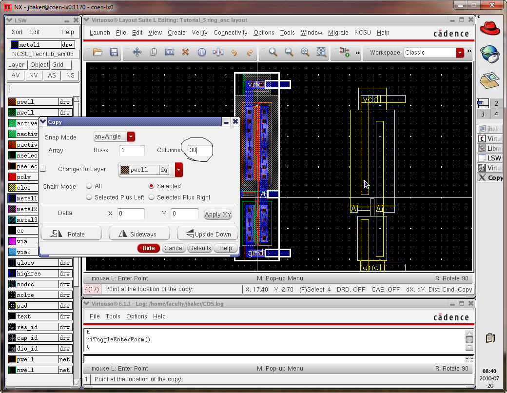
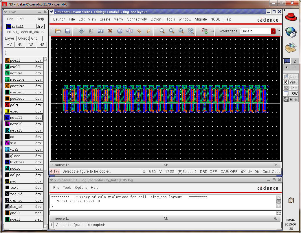
Place
the inverters end-to-end as seen below.
DRC
the layout
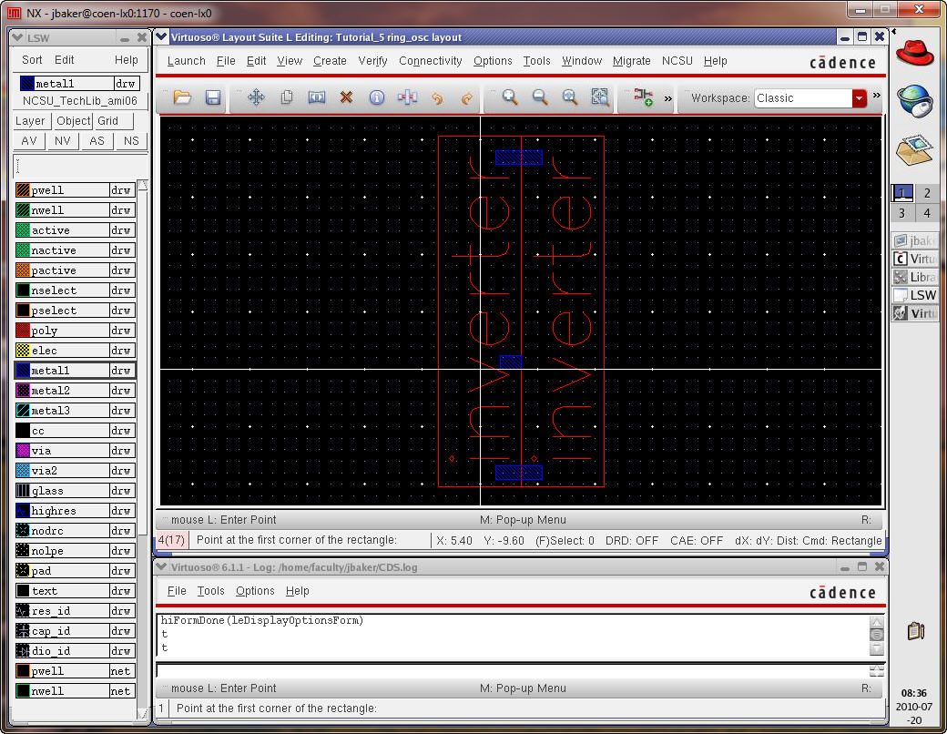
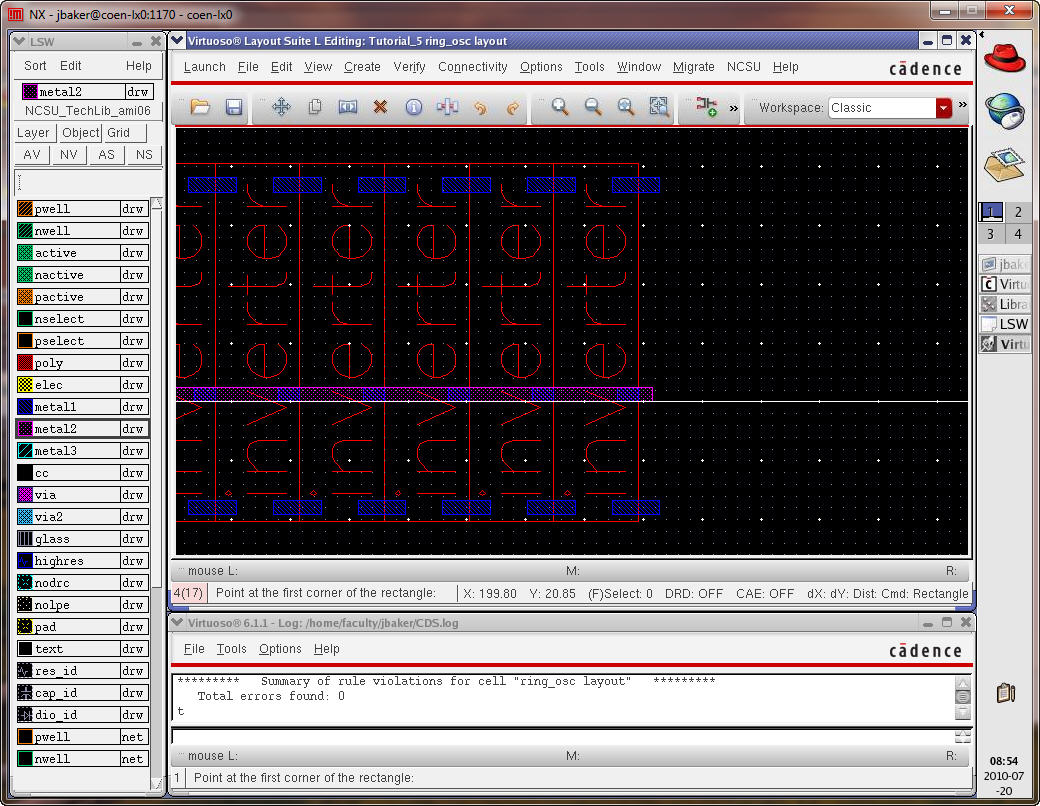
Next
add m2_m1 vias at the
left and
right of the layout as seen below.
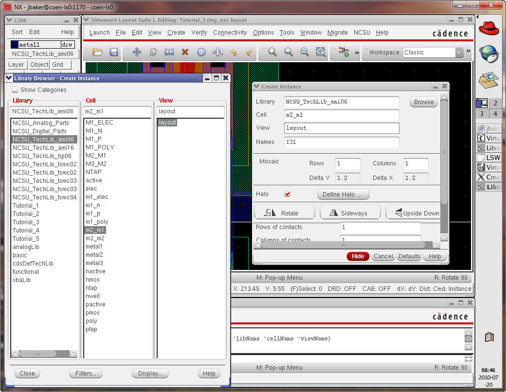
Next
add a rectangle on metal2 connecting these two vias.
Below
is the result where the stop display level is set to 0.
DRC
the layout.
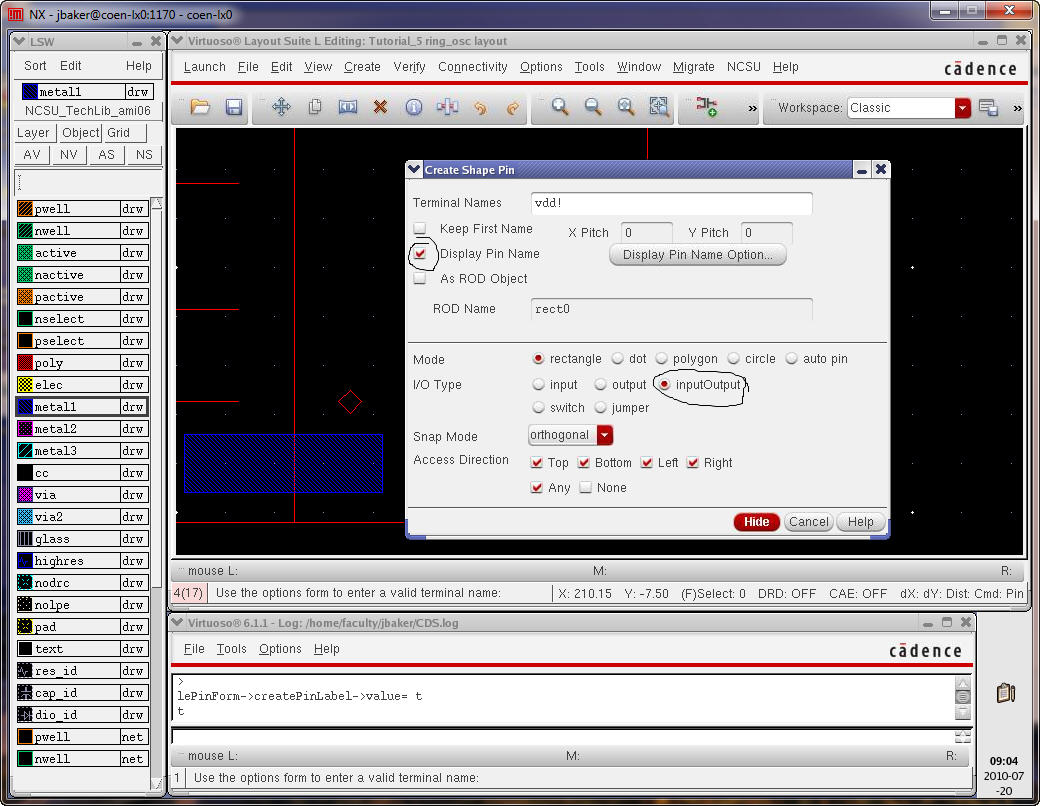
Add
pins for gnd!, vdd! (both have a direction of inputOutput),
and osc_out (set the
direction to output).
Put
vdd! and gnd!
pins on the metal1 layer and osc_out
on the metal2
layer.
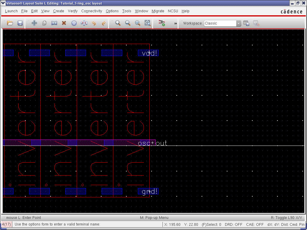
DRC
the layout.
Run
extraction on the layout.
Save
and close the layout view.
Open
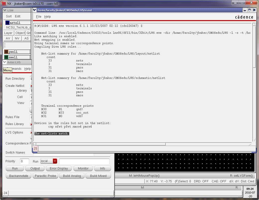
the extracted view and run an LVS.
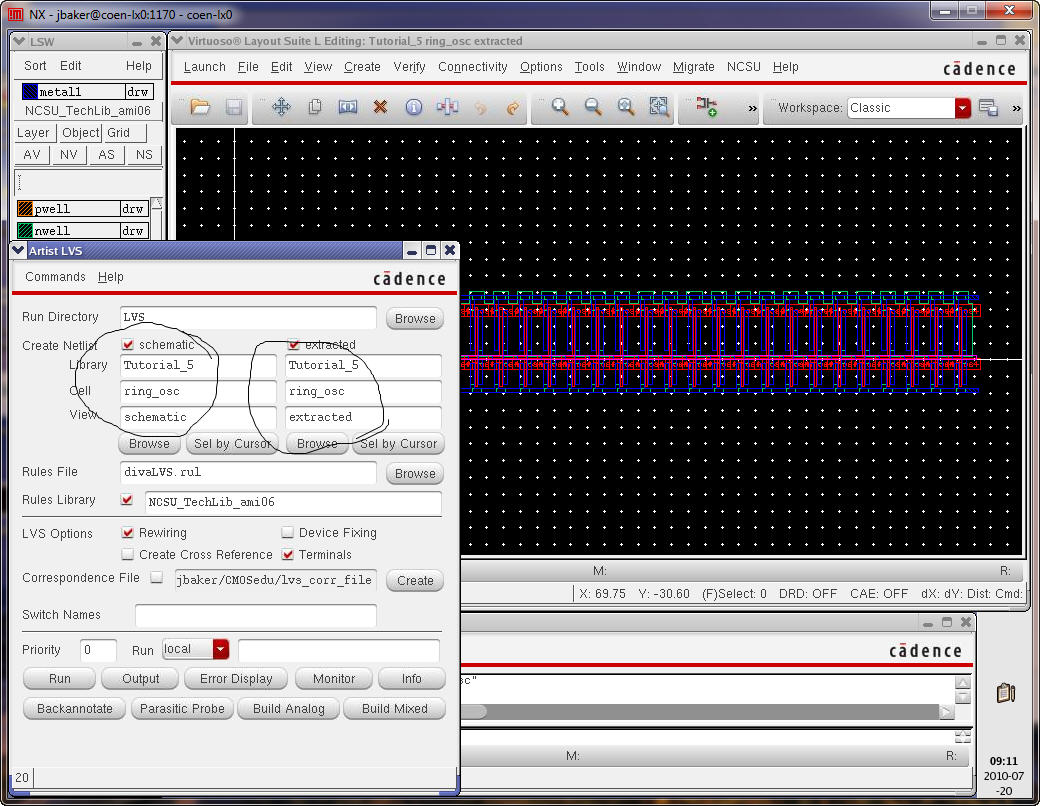
The
LVS fails.
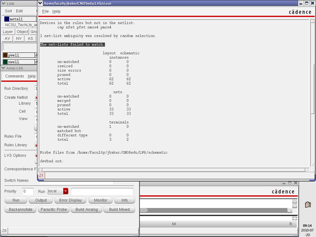
Why?
Looking at the information in si.out
file above we see that terminals are not matched.
We
used a pin for osc_out
in the
layout but not in the schematic.
Let’s
add a pin to the schematic (and then Check and Save).
Make
sure that the pin’s direction is output (so it matches
the layout).
Also
note that the wire connection between the pin and the
bus (wide wire) must be labeled as seen.
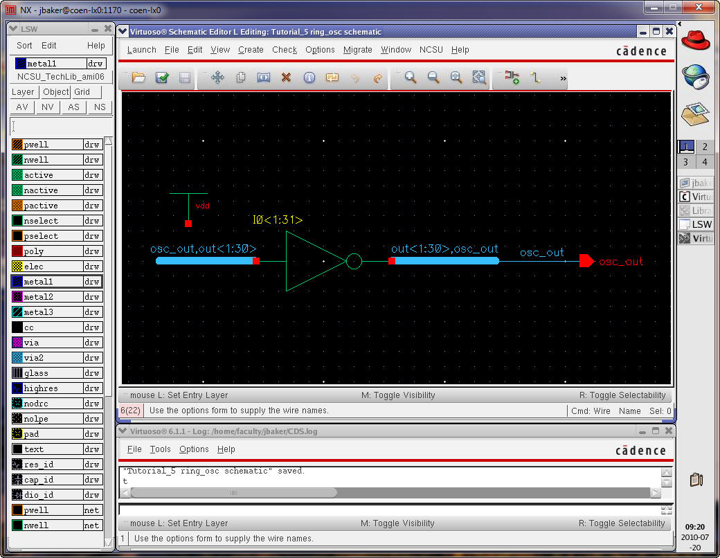
Check
and Save the schematic.
Close
the schematic and open the ring_oscillator’s
extracted view.
Run
the LVS to see that the layout and schematic match.
It’s
useful to compare the simulation results of both a
layout and a schematic.
Delete
the vdd symbol in the
ring
oscillator schematic.
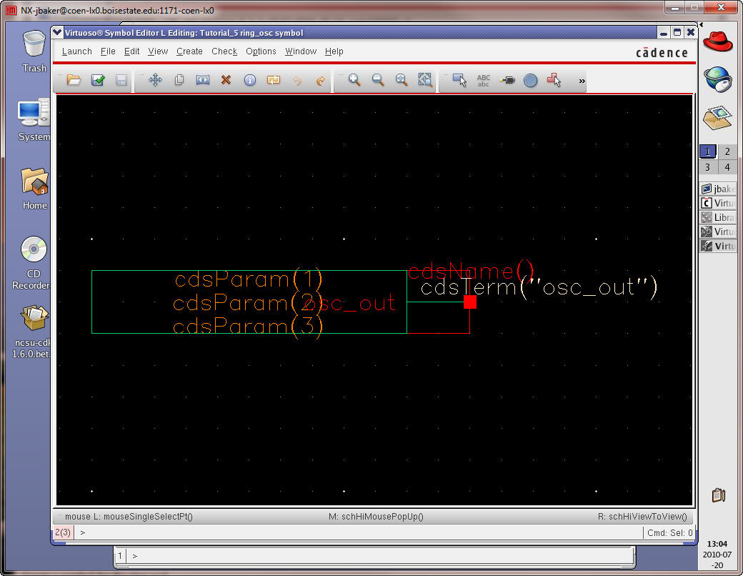
Create
a symbol for the ring oscillator.
Save
and close all cell views.
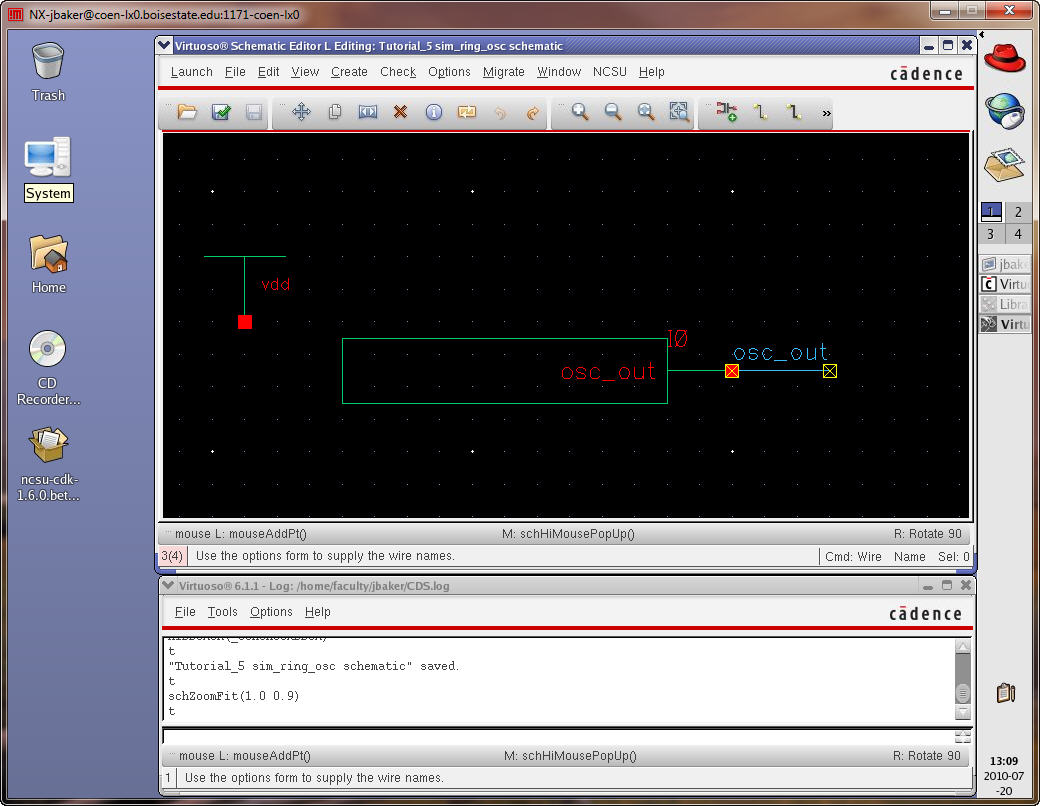
Create
a new schematic cell view call sim_ring_osc.
Please
the ring_osc and vdd symbols in this cell.
Add
a wire to the output of the ring_osc
symbol labeled osc_out
as seen below.
Check
and Save the schematic.
We
get two warnings (floating net/wire)
Use
Check -> Find Markers then press ignore twice and
close the window.
Check
and Save again to verify no warnings/errors.
Launch
the ADE and enter the models, stimuli, outputs to
plot, etc. as we did above.
Don’t
forget to set the osc_out
to
have an initial condition of 0.
When
finished save the state.
Netlist
and Run (hit the green
button) to see the following.
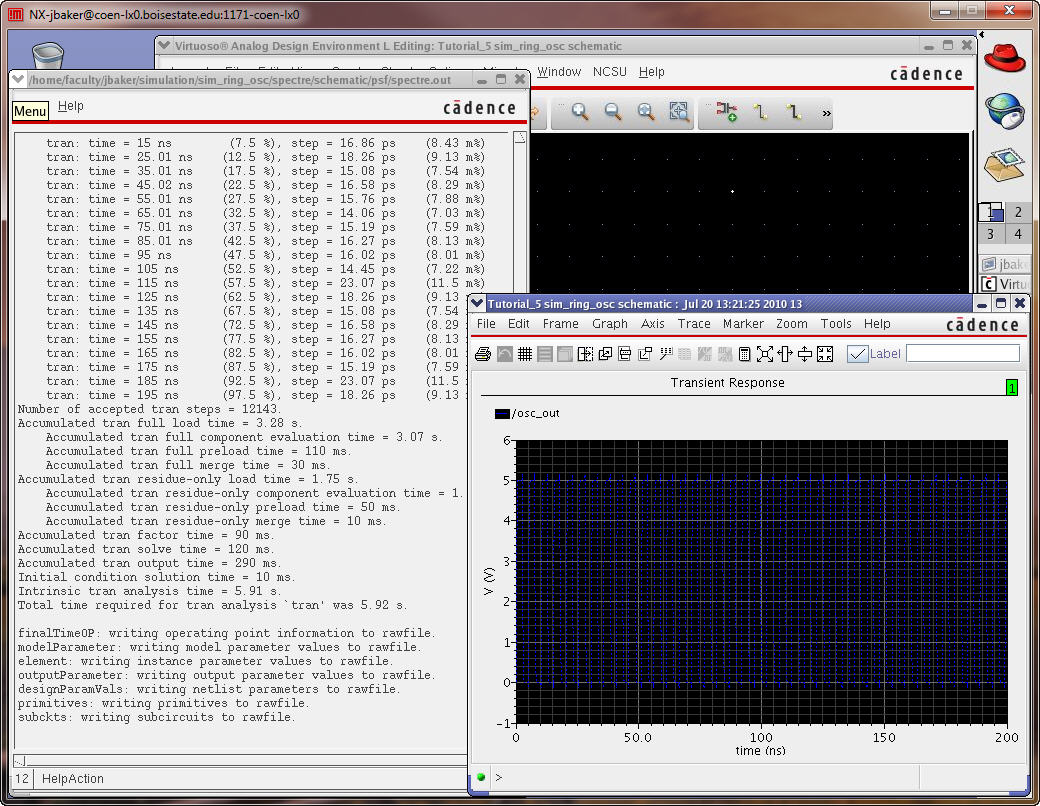
Let’s
simulate the extracted view.
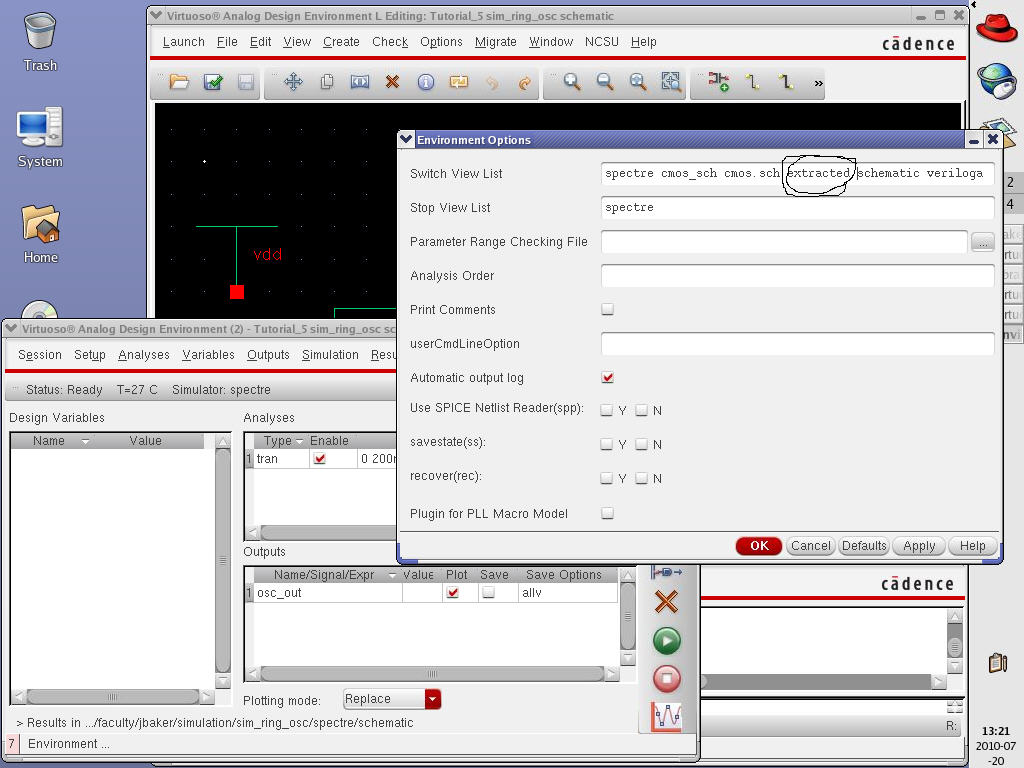
As
before use Setup -> Environment to enter extracted
before schematic.
To
get the following results.
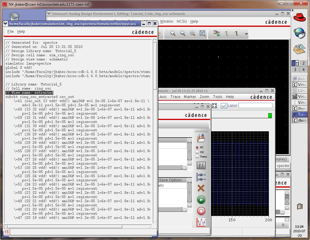
Just
to verify that we are actually using the extracted cell
view use Simulations -> Netlist
-> Display
Save
and close everything.
Remember
that if you save the simulation state with extracted before schematic
(above)
changes to the schematic won’t appear in the simulation results.
Rather
Spectre will continue to
simulate the extracted view.
To fix this simply remove extracted above.
This
concludes Tutorial 5.