Layout of a poly-poly capacitor in the C5 process using the NCSU CDK
Suppose we want to lay out a poly-poly capacitor in the C5 process (AMI 0.6u C5N) using the NCSU CDK.
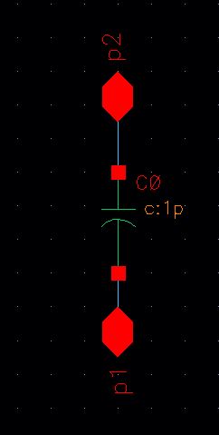
Start by drawing the following schematic.
Use the capacitor from the NCSU_Analog_Parts library.
The
capacitance between poly1 (layer name "poly", the bottom plate, that
is, the plate closest to the substrate) and poly2 (layer name "elec")
is 900 aF/um^2
The NCSU setups may use a different value but 900 is assumed here.
The area that defines a, for example, 1 pF capacitor is W*L*900aF = 1 pF or W = L = 33 um (approximately).
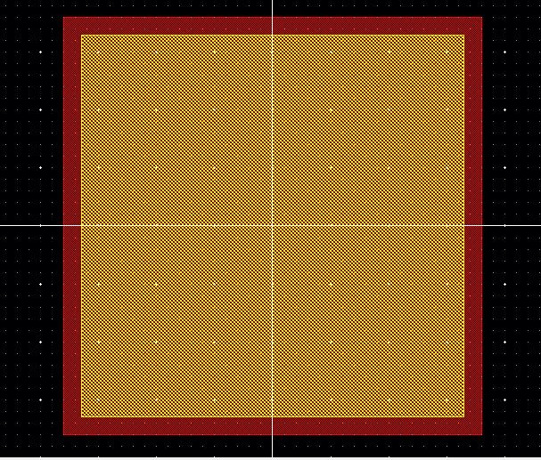
Draw
a rectangle on the "poly" layer that is 36 um square and
another rectangle on the "elec" layer that is 33 um square as seen
below.
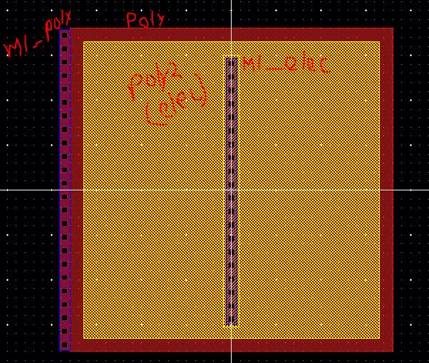
From the NCSU_TechLib_ami06 library add, and edit as seen below, m1_poly and m1_elec cells to the layout.
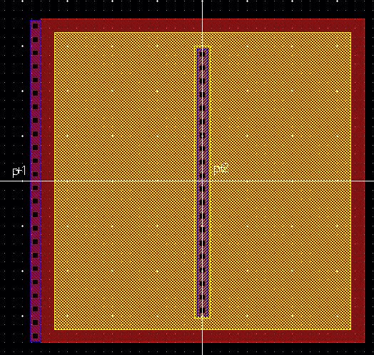
Finally, add pins using metal1 layer for p1 (poly1) and p2 (poly2) as seen below.
DRC (fix errors if you have any) and Extract the layout. LVS to verify that the schematic and layout match.
Note
that the layer cap_id isn't needed. If it is used then the parasitic
capacitance from, say, poly1 to substrate is added to the extracted
view.
The design directory used to generate these figures is found in poly_poly.zip.
Return