Cadence
Design System
Tutorials
from CMOSedu.com (Return)
Tutorial
3 – Design, layout, and simulation of a CMOS inverter
In
this third tutorial we’ll draw the schematic, symbol, and
layout of a CMOS inverter.
We’ll
also simulate the DC behavior of the inverter.
Before
we get going with this tutorial please make sure you
know the answers to the following questions.
If
you don’t, or the answers don’t come to you quickly, then
go back through Tutorial_1
and Tutorial_2
1.
What
does the Bindkey q do?
2.
Which
two Cell Views are
used when doing an LVS?
3.
What
is the difference
between the nmos and
nmos4 schematic cells?
4.
How
do you select the
MOSFET models in the ADE window? What does ADE stand for?
5.
What
is the difference
between moving and stretching?
6.
How
do you layout a
rectangle on the metal1 layer?
7.
What
does the ! indicate
at the end of gnd! and vdd!
8.
What
do the acronyms LSW
and CIW stand for?
9.
How
is the ruler used?
Cleared?
Okay,
hopefully these are easy.
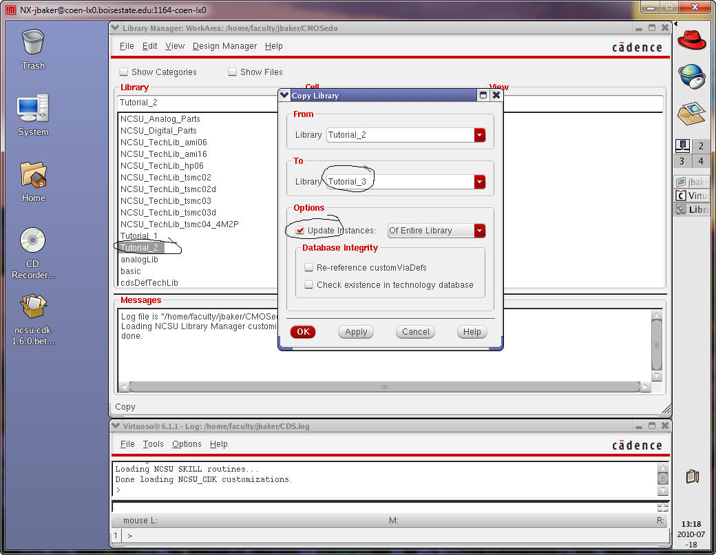
Let’s
start out, assuming Virtuoso has been started in the
CMOSedu directory, by copying the Tutorial_2 library to a library named
Tutorial_3.
Ensure
the new library is placed in $HOME/CMOSedu
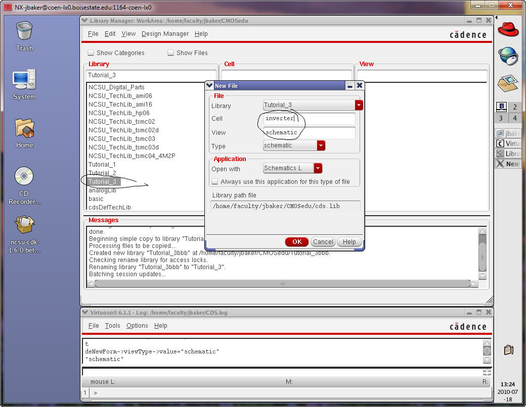
Next
create a schematic Cell View called inverter.
With
this new schematic view open also open the schematic
view of NMOS_IV as seen below.
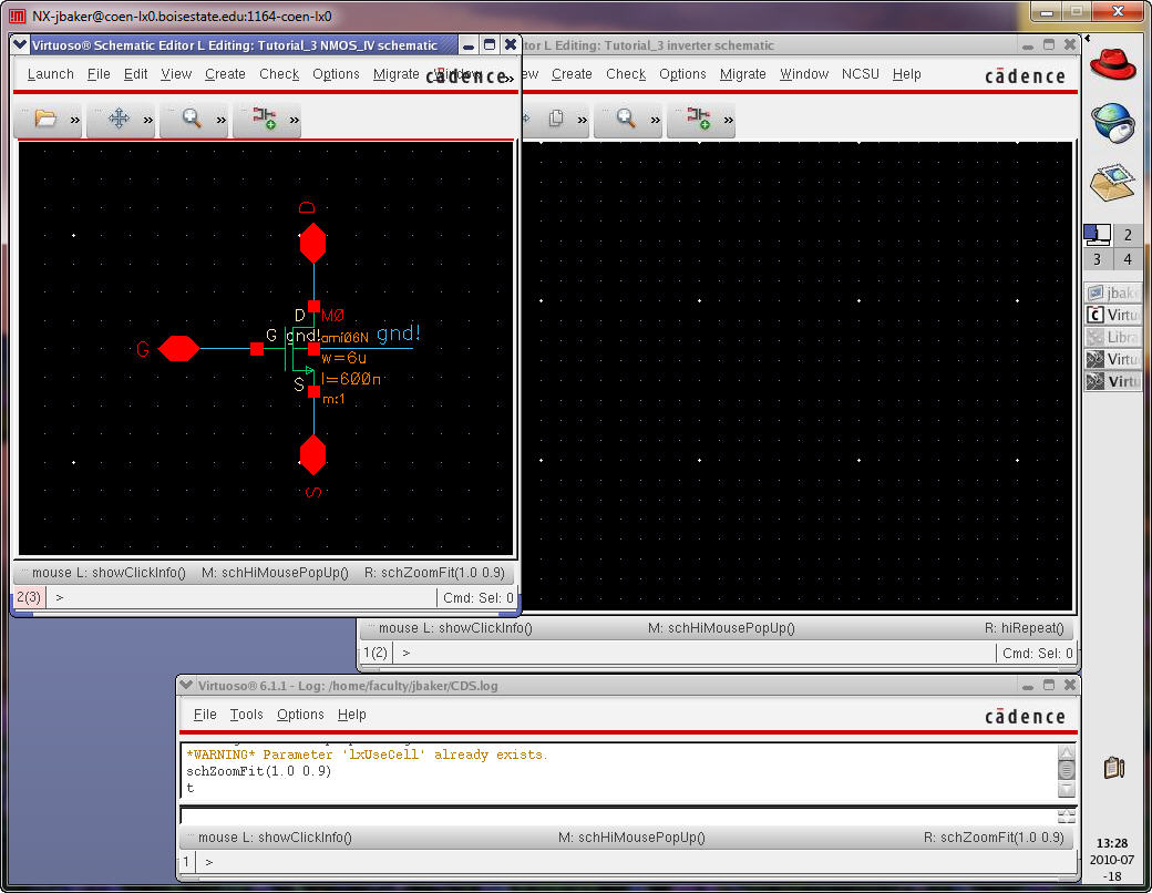
What
we are going to do is copy the NMOS symbol from the
NMOS_IV cell into the inverter cell.
To
do this we need to have both windows open (no clipboard
that we can copy items to).
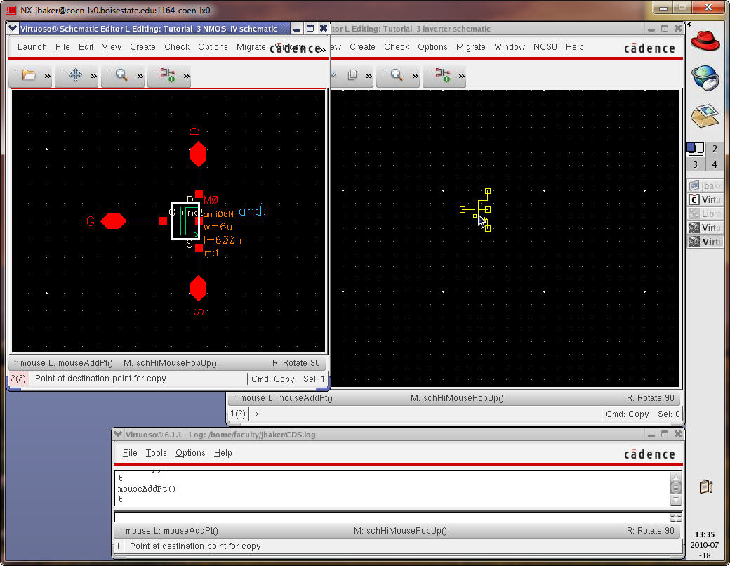
Press
the copy Bindkey c (or use the menu) then click on the
nmos4 symbol and drag over into the inverter window (and click the left
mouse
button to instantiate).
Close
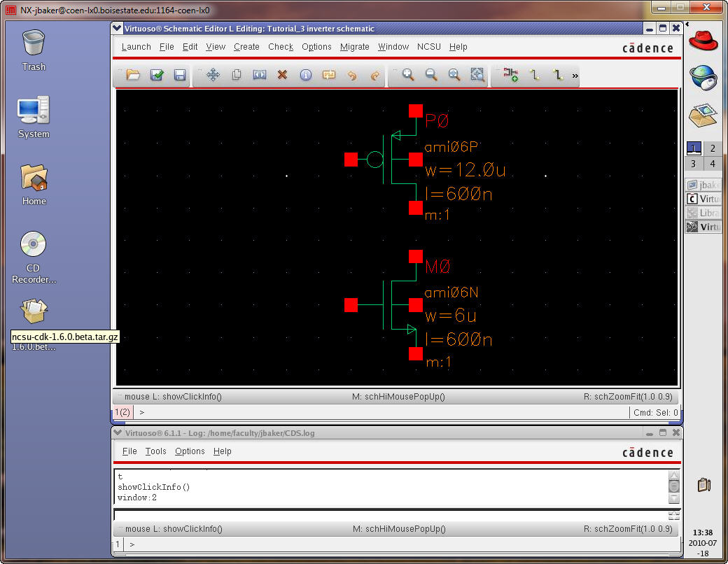
the NMOS_IV window and open the PMOS_IV window.
Repeat
for the pmos4 cell to get the following.
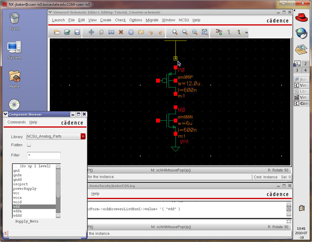
Instantiate
vdd and gnd supply nets.
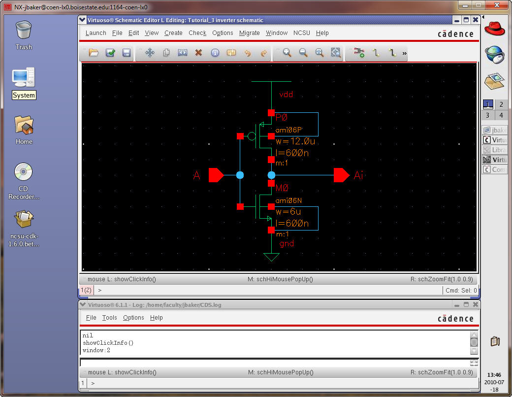
Finally,
wire up the inverter and add pins as seen below.
The
A pin should have an input direction and pin Ai should
have an output direction.
Next
use the menu items to Create -> Cell View -> From
Cell View to create the symbol for the inverter.
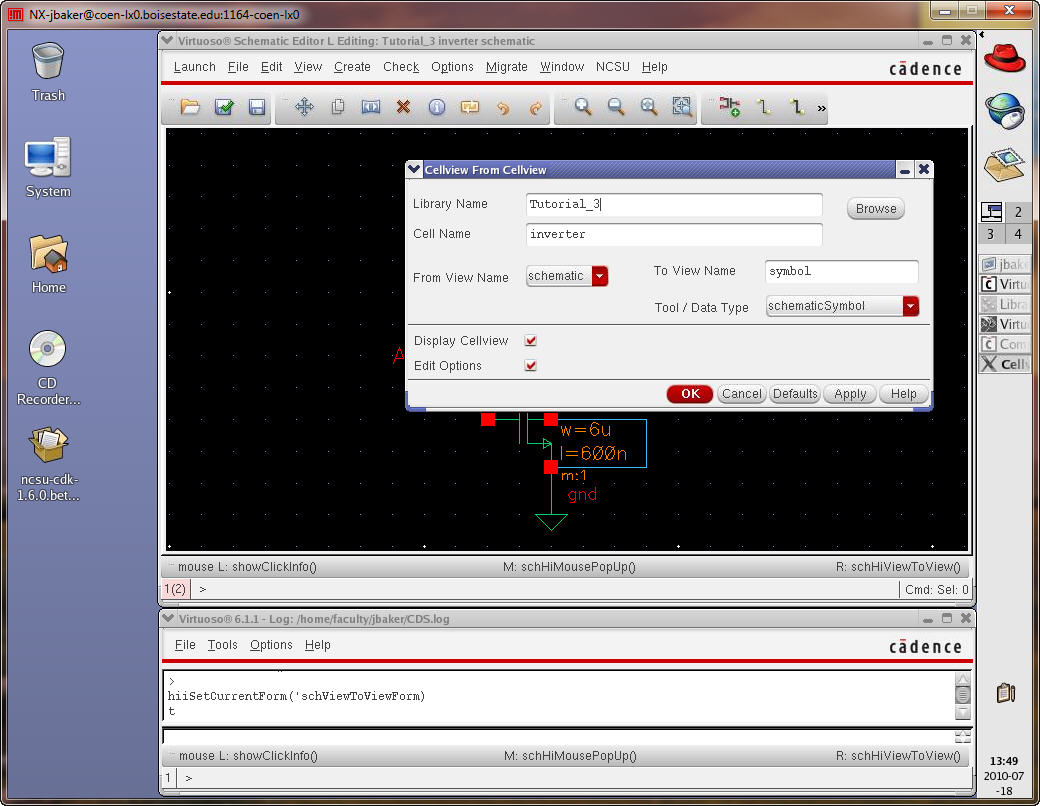
Select
OK (twice).
Check
and Save the schematic view of the inverter (and then
close this window).
Delete
everything in the inverter’s symbol view except for
the pins.
Draw
the inverter symbol seen below (Create -> Shape ->
Line/Circle)
Since
we aren’t showing the pin names select the pin and
verify that it’s in the right location (A is an input Ai is the
inverter’s
output)
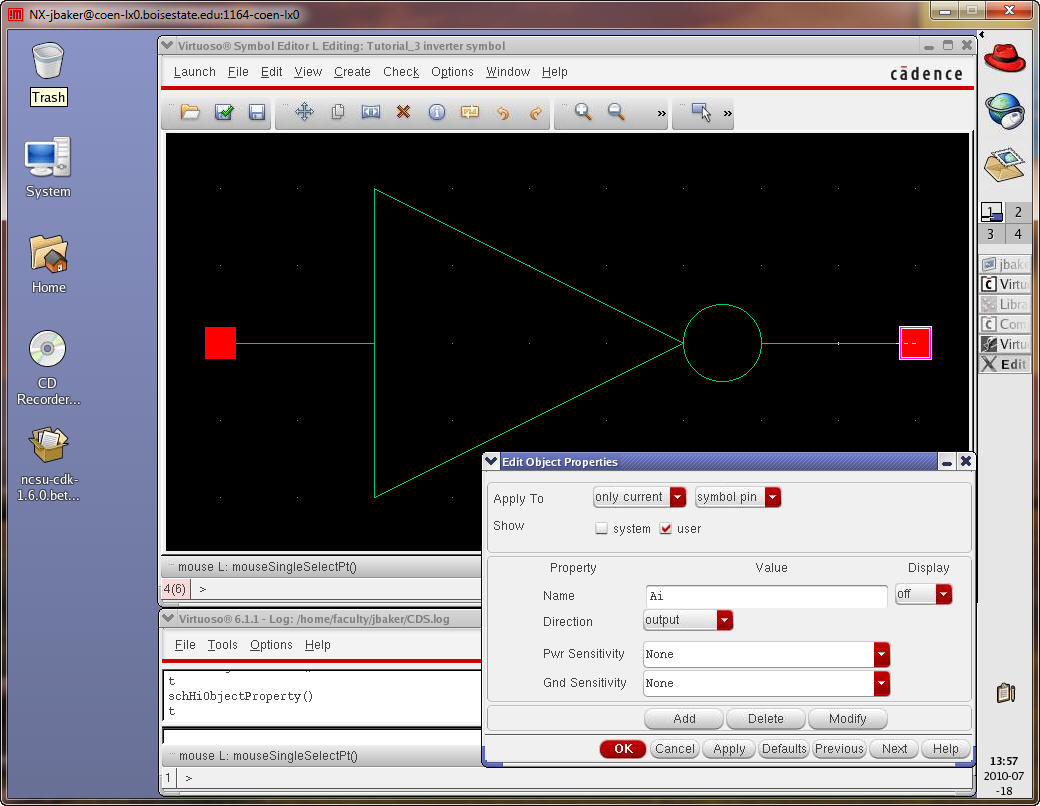
Check
and Save the inverter symbol.
Next
Create the layout view for the inverter.
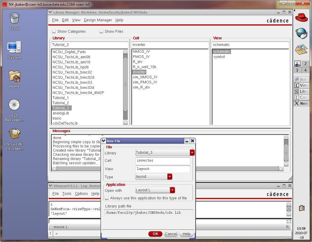
Add
the following cells (nmos,
pmos, ntap, ptap,
and m1_poly) to this layout view as seen below (you can copy as before
but here
we will instantiate cells).
Ensure
the nmos is 6u/0.6u and
pmos is 12u/0.6u and the
ntap and
ptap use two columns.
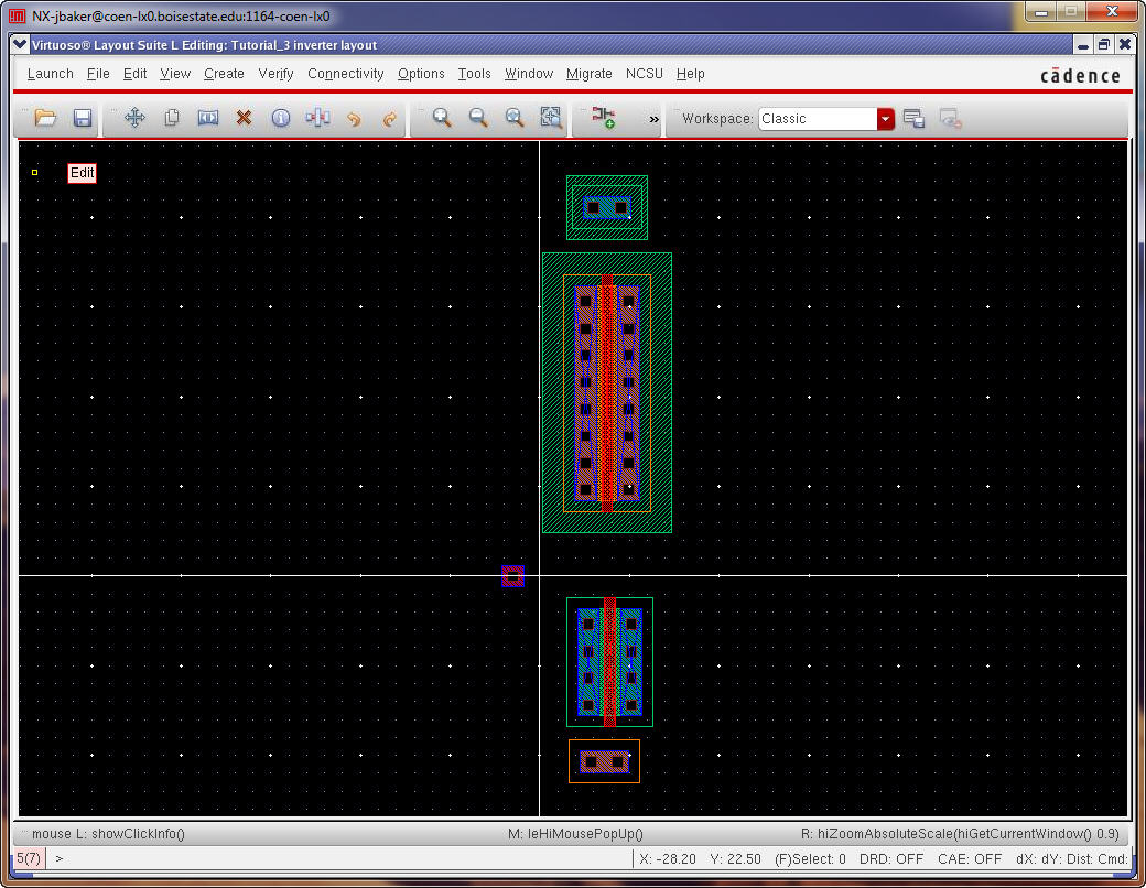
Next
align the cells until you get something similar to what
is seen below.
DRC
your layout to ensure no errors (fix as needed).
Save
the layout.

Add
rectangles on poly and metal1 as seen below.
DRC
and save your design.

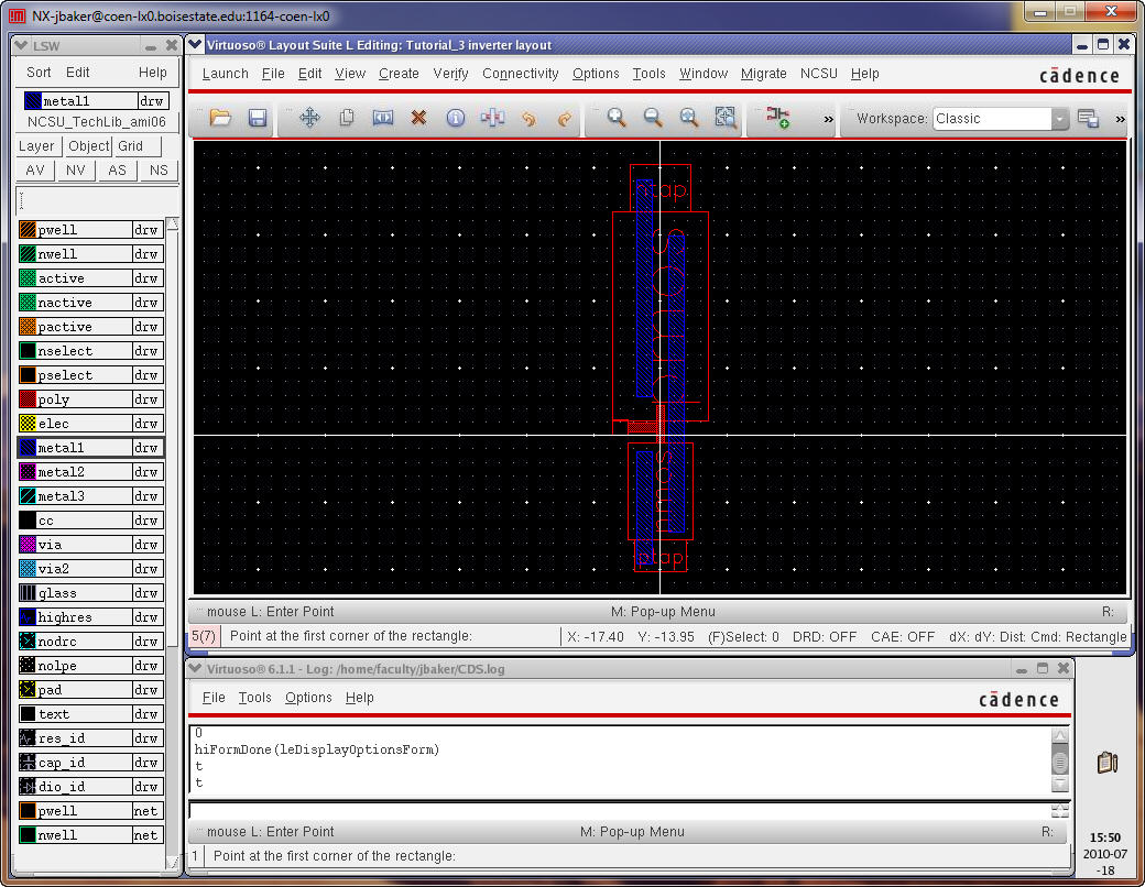
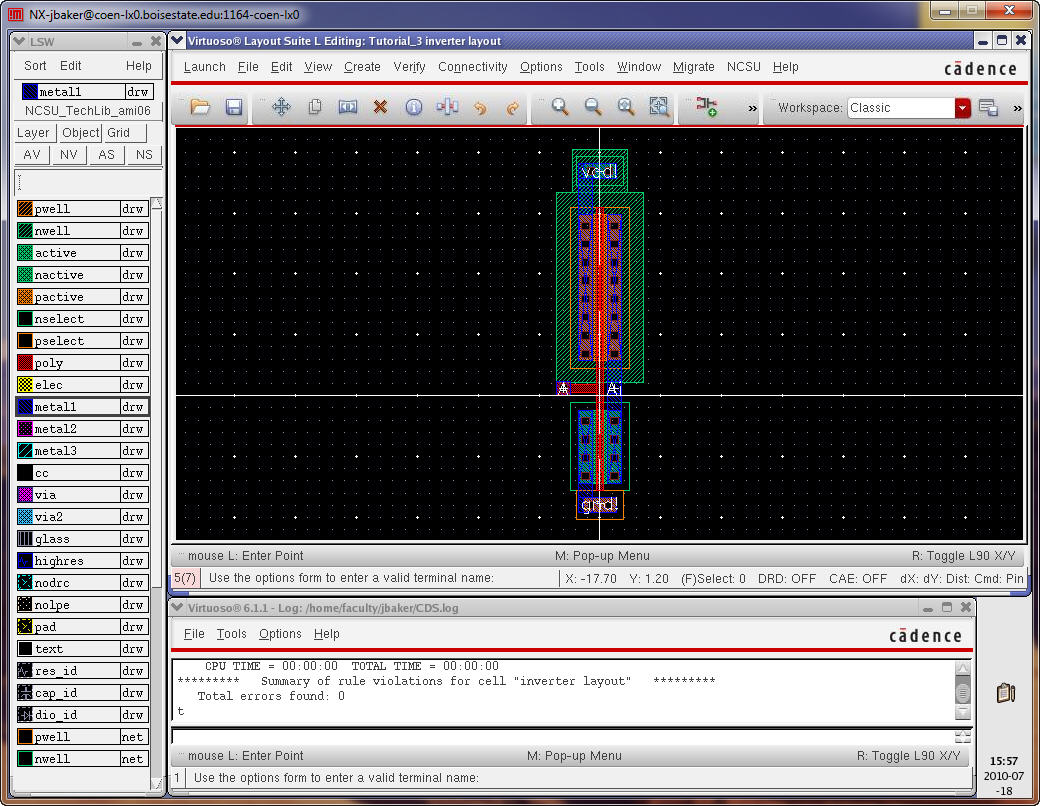
Next
add pins on metal1 for gnd!,
vdd! (both have a
direction of inputOutput),
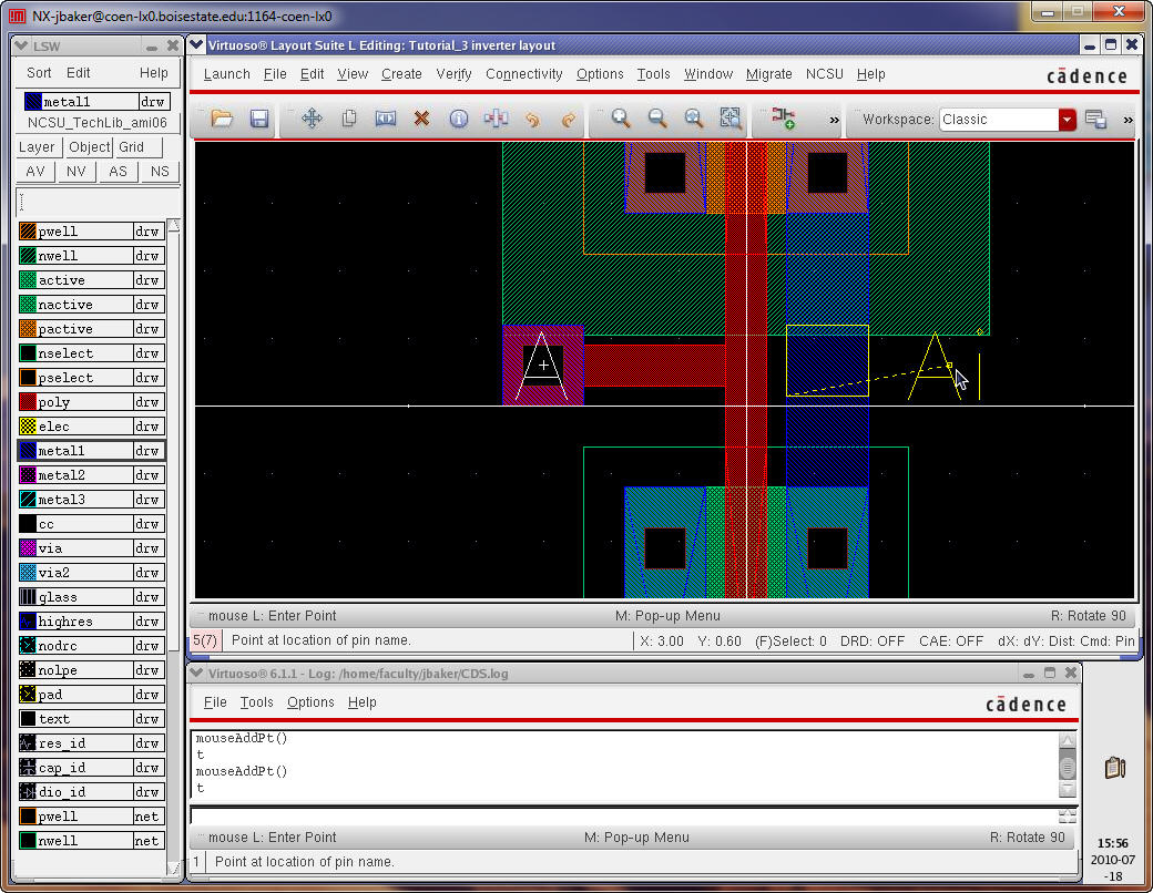
A (input), and Ai (output).
DRC
and save the design.
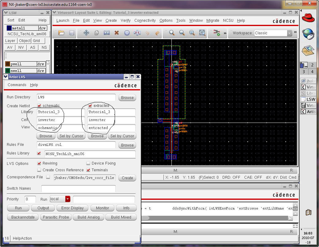
Next
run extraction on the layout.
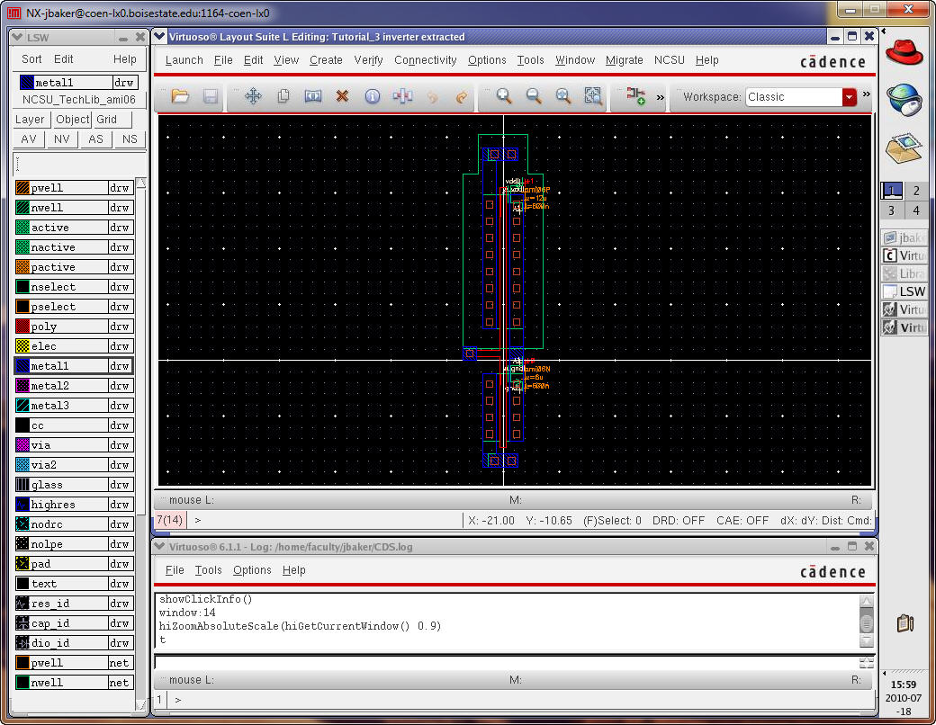
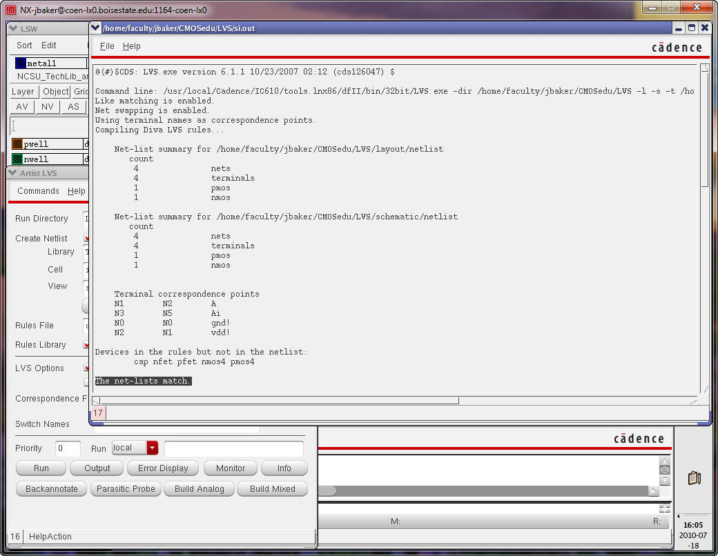
Finally,
run the LVS on the inverter.
Okay,
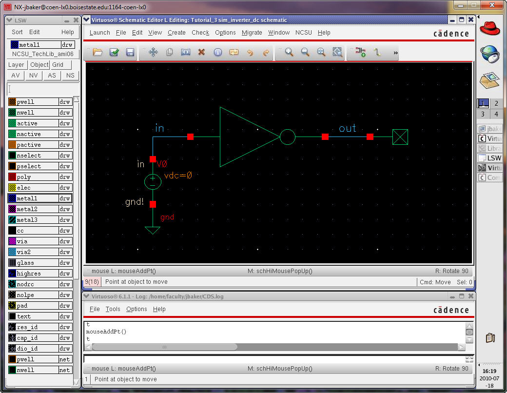
we are ready to simulate the operation of the inverter.
Create
a cell called sim_inverter_dc
(File -> New -> Cell View)
Draft
the following schematic.
The
symbol on the right is the no-connection symbol (in the
basic library, Misc -> noConn)
We add this symbol
to be different and to avoid getting the warnings
related
to floating pins/nets that we ignore via the menu
items Check -> Find Marker -> ignore, ignore
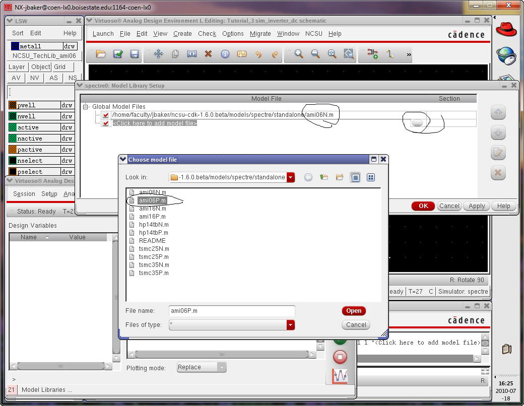
Start
the ADE and select the model files (Setup -> Model
Libraries located in /$HOME/ncsu-cdk-1.6.0.beta/models/spectre/standalone)
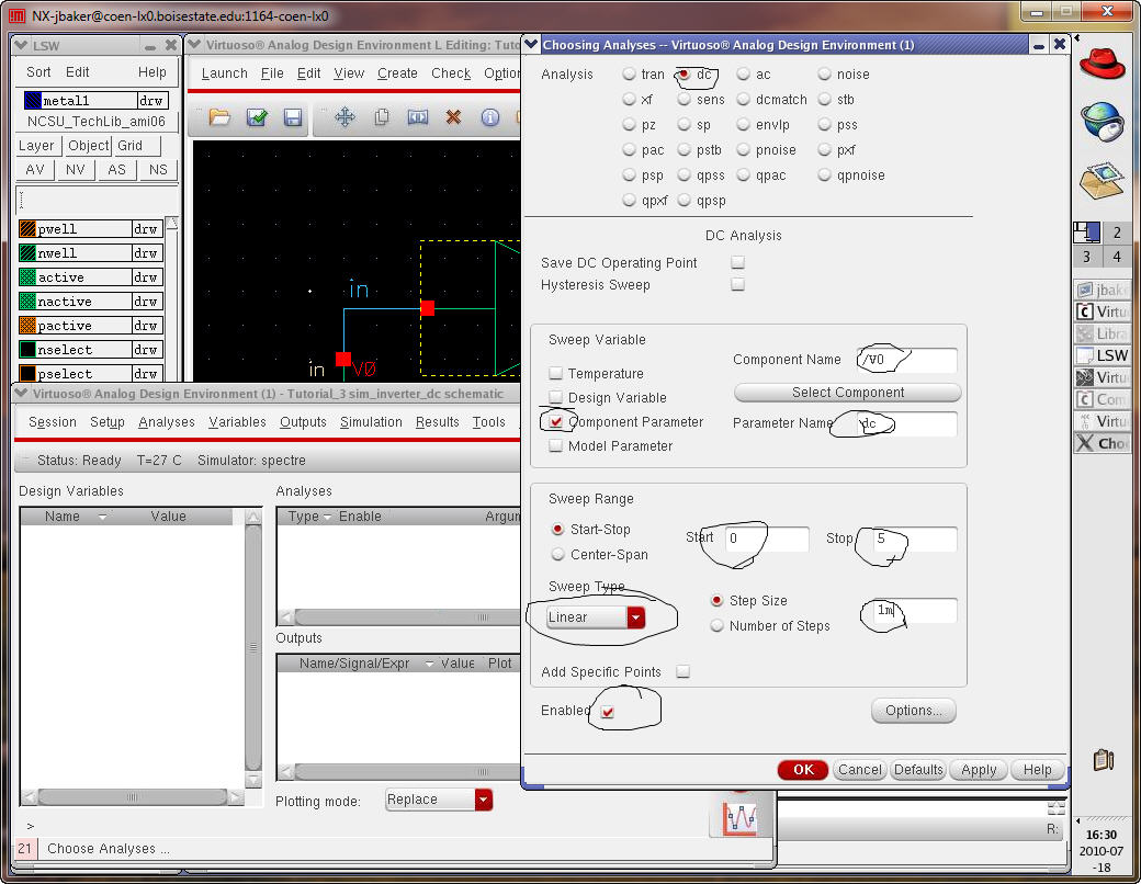
Next
select Analyses -> Choose
Note
that the input vdc is
named
V0.
Next
go to Outputs -> To Be Plotted -> Select On
Schematic (select in and out)
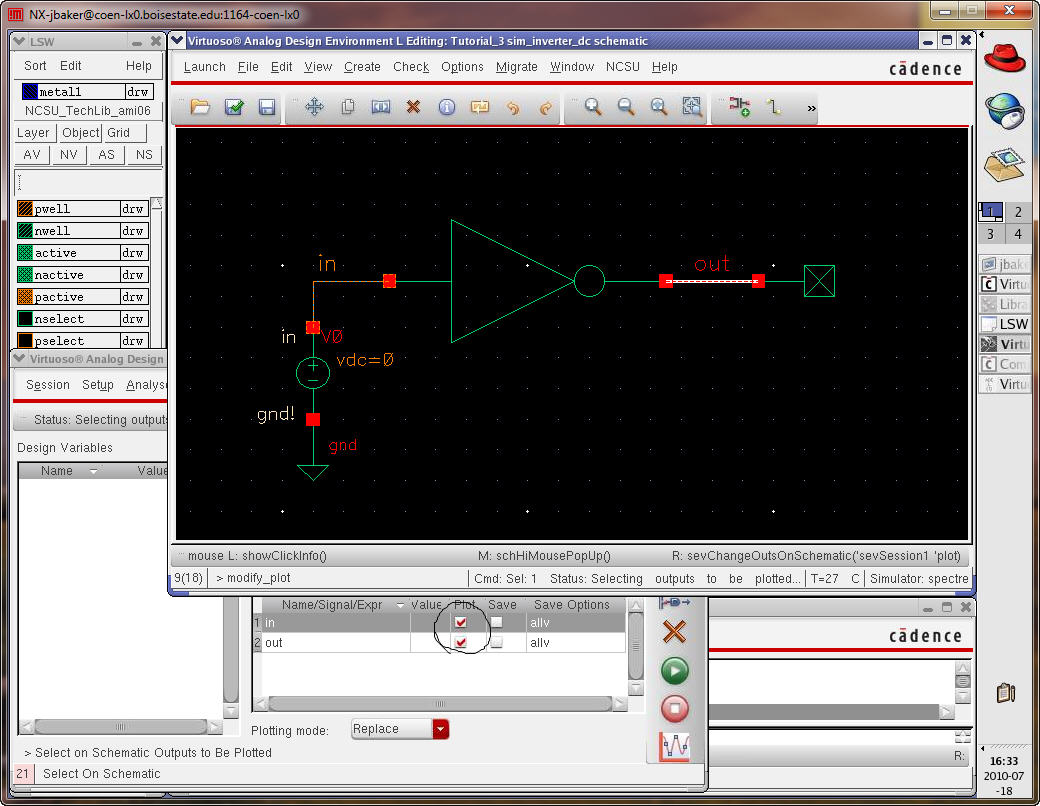
Save
the state in the cellview.
Netlist
and Run the simulation
(hit the green button).
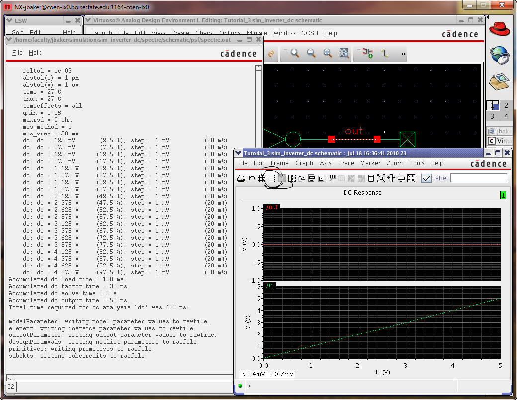
We
get the results seen below.
The
“Strip Chart Mode” was used to display the results
(circled menu item).
Note
how the output is zero!
Well,
we didn’t specify a vdd!
anywhere so it should be zero. Let’s fix this.
Let’s
add vdd as seen below.
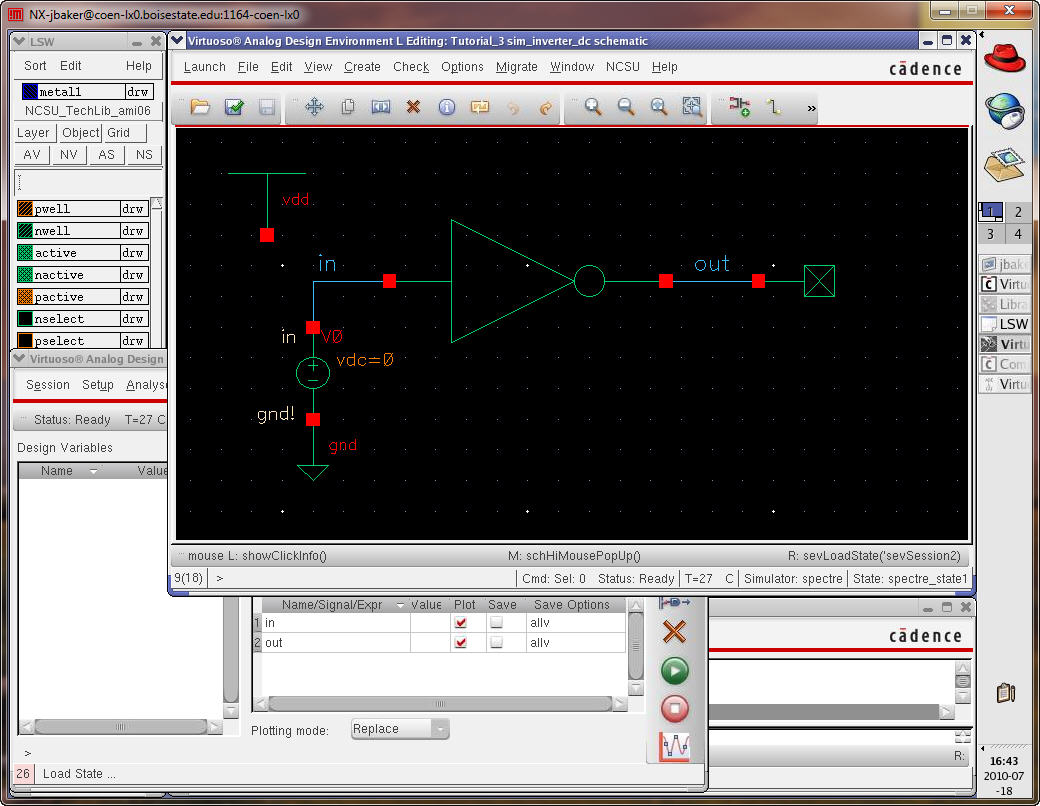
Check
and Save the schematic. Note that if the inverter and vdd symbols overlap there will
be errors when you Check and
Save (so don’t put vdd
too
close
to the inverter symbol).
Next, in the ADE, select Setup -> Stimuli and the parameters seen below (after hitting the Apply button).
If
you directly add a voltage source to your schematic like the
following, 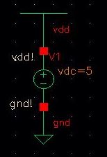 , you should NOT
also use a Stimuli (Global source) since the result is two voltage
sources connected to the same node (which will result in error and the
simulation not running!)
, you should NOT
also use a Stimuli (Global source) since the result is two voltage
sources connected to the same node (which will result in error and the
simulation not running!)
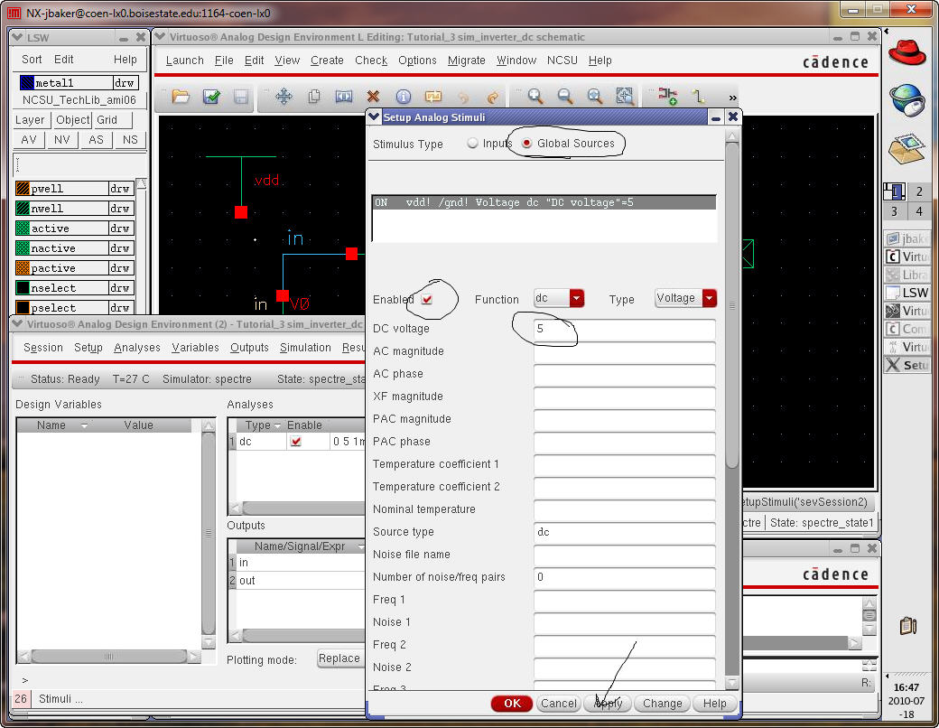
Save
the state (Cellview) so
we
don’t have to do this again next time we run the simulation.
Hit
OK and run the simulation.
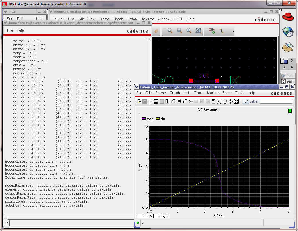
The
results are what we expect the inverter voltage transfer
curves to look like.
Let’s
go ahead and simulate the extracted layout at this
point (Setup -> Environment
and add extracted in
front of schematic as discussed in the last tutorial).
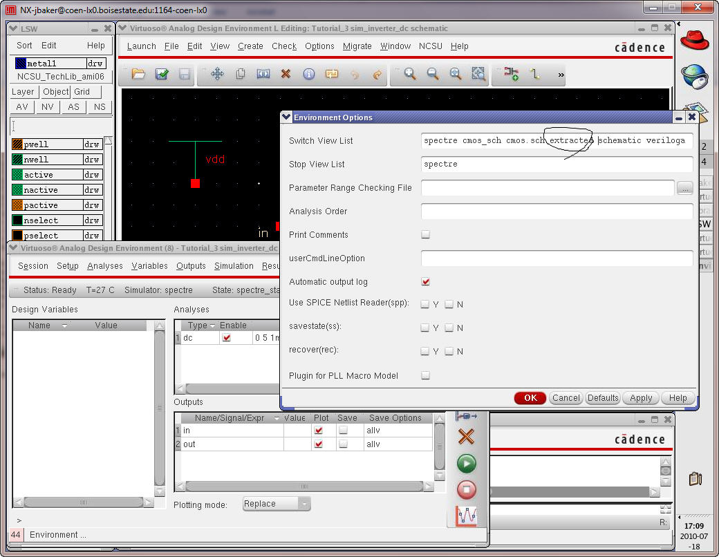
Which
gives the same results as the schematic.
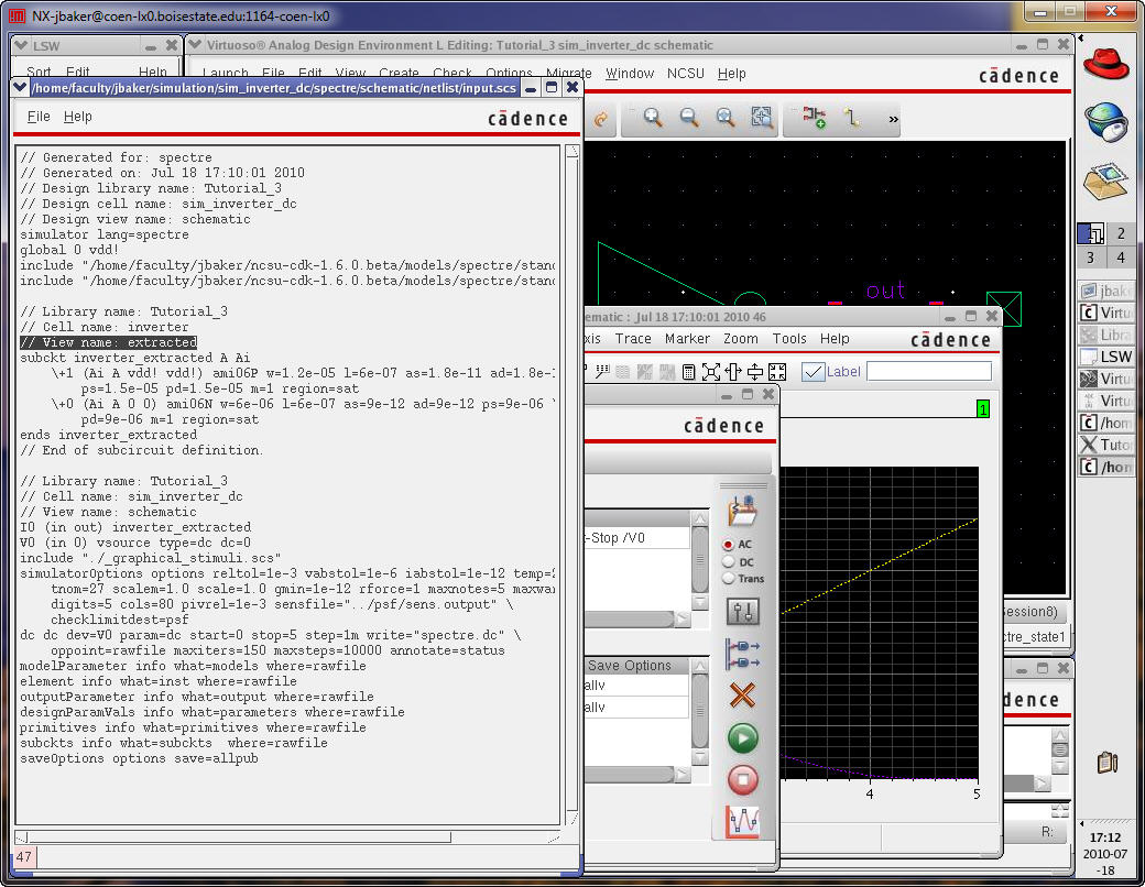
To
verify we are simulating the extracted view and not the
schematic view go to Simulations -> Netlist
->
Display
Save
and close everything. This concludes Tutorial 3.
For
your reference the Tutorial_3 directory is available in Tutorial_3.zip.