Bryan Kerstetter
Electrical Engineer
 Webpage
Last Updated May 2020
Contact Information:
Email: bdkerstetter@gmail.com
About:
In May 2020, I graduated from UNLV with a bachelor’s degree in
Electrical Engineering. After graduating, I started working at Micron Technology in Boise as a DRAM Design
engineer. While at UNLV I was an
Undergraduate Research Assistant underneath Dr. R. Jacob Baker in his
research laboratory. While working in the laboratory, I gained experience in
PCB design, SMD soldering, testing, debugging, wire bonding, and IC layout in
both ON Semiconductor’s C5 and TowerJazz’s SBC18HA
processes. I also worked underneath Dr.
Grzegorz Chmaj as a Laboratory Assistant to help
maintain UNLV’s electronics laboratories. Throughout my undergraduate career, I
had the opportunity to participate in many projects. Notably, I designed a 32x32 APD Camera System Board and a AVR Development Board PCB that is used for embedded
systems classes at UNLV. I also taught a PCB
workshop and gave PCB lecture. My favorite
classes were Analog
IC Design, Digital
IC Design, and Memory Circuit
Design.
This webpage features the highlights of my undergraduate career.
To see what I am up to now, please visit bryankerstetter.com
or my LinkedIn
profile.
Laboratory
Reports:
·
EE 420
Analog Integrated Circuit Design Laboratory
·
EE 421
Digital Integrated Circuit Design Laboratory
Significant
Course Projects:
·
ECG
721: The Design of a Variable DPLL Clock Multiplier (A Tutorial Presentation)
·
EE
421: CMOS Boost Switching Power Supply in the C5 Process
·
EE
421L: CMOS 4x Clock Multiplier
· EE 420L: Design and Implementation of a Voltage Amplifier
Paper Presented at the GLSVLSI 2019 ACM Great Lakes Symposium May
9-11, 2019:
·
Monolithic
8x8 SiPM with 4-bit Current-Mode Flash ADC with Tunable Dynamic Range
Senior Design Project:
·
SeeBlik
(Underwater Optical Communication System), Poster
Calculator Useful for Circuit Design:
·
IC
Resistor Geometry Calculator
PCB Presentation:
·
An
Introduction to PCB Design Presentation
Webpage Contents:
EE 498: PCB Design Lecture (March 11, 2020)
IEEE
PCB Design Workshop (March 2019)
1. Digital Phototransistor Optoisolator
(DPO) and Its Respective Applications
2. 32x32
APD Camera System Board
3. IC Resistor Geometry
Calculator
4. VDDS Test Board for the
Voyager Chip (APD/SiPM read-out circuits and digital SiPM)
5. Current Mode ADC PCB for the
Solar Sailor (SiPM ROIC) Chip.
6. UNLV ECE AVR Development
Board Rev. 2
7. Designed and Milled
Electronic Piano PCB
CMOS 4x Clock Multiplier with Voltage Controlled Delay Elements
Click Image for Larger Image
EE 498: PCB Design
Lecture (March 11, 2020)

Electronic Piano PCB
I taught PCB design lecture
for EE 498 Senior Design 2. At UNLV, senior engineering students spend two
semesters working on a capstone project. For the second semester, electrical
and computer engineering students are expected to design and have a PCB
fabricated for their project. Often, this is the first time many are faced with
designing a PCB. The lecture that I taught introduced students to the basics of
PCB design. I also demonstrated how to use Autodesk Eagle PCB
Design Software, designed a PCB in class, and gave advice on how to get
PCBs fabricated. I also brought an
Electronic Piano PCB into class that I had designed and soldered for an
interactive example.
An
Introduction to PCB Design Presentation
PCB
Design Lecture Resources ← (Click link to access PCB designed in
class)


IEEE PCB Design Workshop
(March 2019)
I taught a PCB workshop for the UNLV IEEE student chapter. During
the workshop, I explained how to use Autodesk Eagle PCB
Design Software. By the end of the workshop, everyone that followed along
was able to design a LM555 Electronic Piano PCB. All the final design files and
workshop resources can be viewed at the following link.
Design
Files and Workshop Resources

Electronics Projects
1.
Digital Phototransistor Optoisolator
(DPO) and Its Respective Applications


The project was awarded 1st Place in the Fall 2018 Junior Design
Competition. David
Santiago and I are pictured below at the competition.


2. 32x32 APD Camera System
Board
Microcontroller Board
and Camera Platform Design by Bryan Kerstetter
Highlights:
·
ATMEGA328PB
·
5V and 3.3V Power
Regulation
·
ISP for Programming
·
USB Mini B and UART
for Data Output
·
Shutter and Reset
Buttons
·
Various Indicator LEDs
Imaging Chip Designed
by James Mellott
Software by Chris Barr
Image Processing by David Santiago
3D
Printed Canon FD Lens Mount by Daniel Senda
Camera Core PCB by James Skelly
3D Printed Camera Core
Spacer by Francisco
Mata-carlos


3.
IC Resistor Geometry Calculator
Coded in HTML and
JavaScript. Developed while taking EE 421: Digital Integrated Circuit Design to
alleviate IC resistor calculations.
4. VDDS Test Board for the Voyager Chip (APD/SiPM read-out circuits and digital SiPM)
Chip
Designed by Vikas
Vinayaka


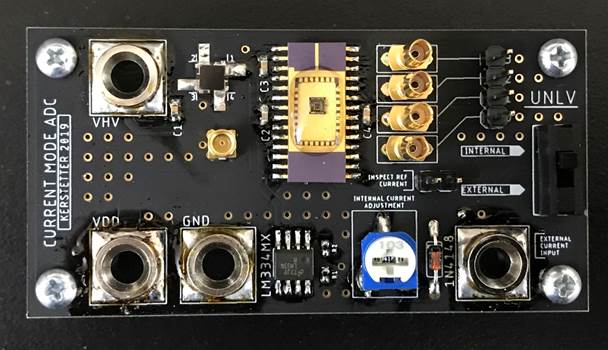
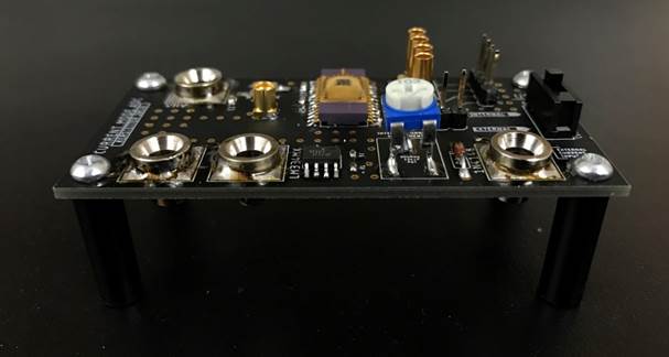
5. Current Mode ADC PCB for the Solar Sailor (SiPM ROIC) Chip
Chip
Designed by Vikas
Vinayaka
The PCB contains an internal adjustable constant current source
circuit (7-12µA) that was created by modifying the LED
Driver circuit. Alternatively, an external current source can also be
used.


6. UNLV
ECE AVR Development Board Rev. 2
Circuit
Designed by Binayak
Tiwari
An embedded systems development board that utilizes an ATMEGA328P
microcontroller. The board features a keypad, 4 push button array, 8-pin
dipswitch, buzzer, 8 LED Array, and an LCD header among other features. The development
board is used in CPE 301L
and CPE
310L at the UNLV Department of Electrical and Computer Engineering.


7. Designed and Milled Electronic Piano PCB
Milled
on a Bantam
Tools Desktop PCB Milling Machine


Return to Dr. Baker’s CMOSedu homepage


