ECE 421L Digital Integrated Circuit Design Lab
| Lab1 | Laboratory introduction, generating/posting html lab reports, installing and using Cadence. |
| Lab2 | Design of a 10–bit digital–to–analog converter (DAC). |
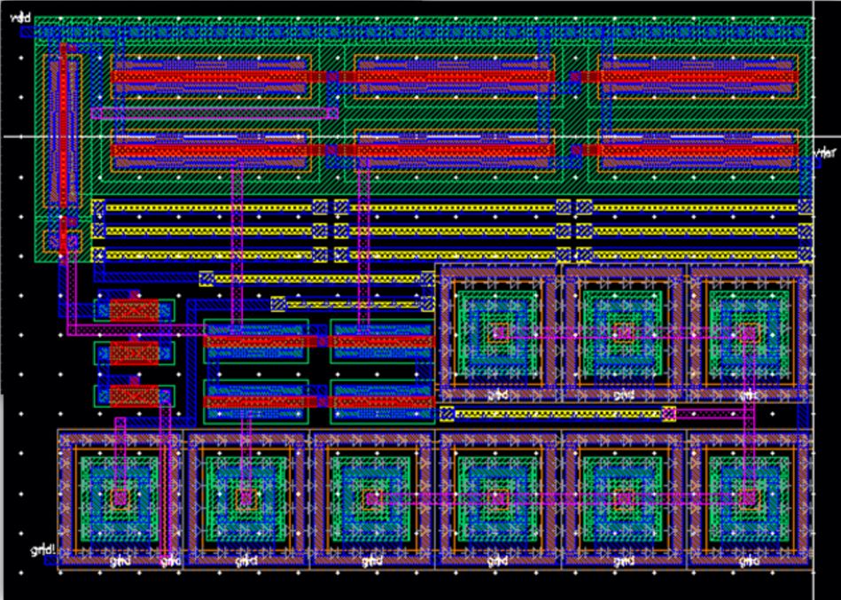
| Lab3 | Layout of a 10–bit DAC. |
| Lab4 | IV characteristics and layout of NMOS and PMOS devices in ON's C5 process. |
| Lab5 | Design, layout, and simulation of a CMOS inverter. |
| Lab6 | Design, layout, and simulation of a CMOS NAND gate, XOR gate, and Full–Adder. |
| Lab7 | Using buses and arrays in the design of word inverters, muxes, and high–speed adders. |
| Lab8 | Generating a test chip layout for submission to MOSIS for fabrication. |
| Project | Design an even parity checking circuit having a 9-bit input word, 8-bits data and 1-bit parity. |