Project - EE 421L
Authored by Surafel Abera
Abera@unlv.nevada.edu
November 15, 2017
First Part of Lab Work:Design
an even parity checking circuit having a 9-bit input word, 8-bits
data and 1-bit parity, that outputs a 1 (0) when the even parity check is valid (invalid)
The inputs to your circuit are D0-D7, P and the output is checkd.
An
even parity bit is a bit added to a string of binary code to
ensure that the total number of 1-bits in the string is even.
An odd parity bit is a bit added to a string of binary code to
ensure that the total number of 1-bits in the string is odd
| 8 bits of data | count or (#) of 1-bits | 8 bits (+) parity bit = 9bits |
| even | odd |
| 0000 0000 | 0 | 000000000 | 000000001 |
| 1010 0000 | 2 | 101000000 | 101000001 |
| 1000 1110 | 4 | 100011100 | 100011101 |
| 0000 0001 | 1 | 000000011 | 000000010 |
| 1001 0001 | 3 | 100100011 | 100100010 |
| 0011 1110 | 5 | 001111101 | 001111100 |
The
even parity checking circuit will be checking the validity of the 9-bit
input word by comparing the parity bit (the las bit) with 8-bit parity
generator.
An
even parity bit (1-bit) is generated from 8-bit input XOR gate and it
is XORed with the 9th bit (last bit). The output tells us the validity
of the 9th bit.
| D2 | D1 | D0 | P |
| 0 | 0 | 0 | 0 |
| 0 | 0 | 1 | 1 |
| 0 | 1 | 0 | 1 |
| 0 | 1 | 1 | 0 |
| 1 | 0 | 0 | 1 |
| 1 | 0 | 1 | 0 |
| 1 | 1 | 0 | 0 |
| 1 | 1 | 1 | 1 |
P(3-bit) = (D2) XOR (D1) XOR (D0)
Schematic and Symbols for inverter, buffer, XOR Gates
| inverter Schematics | inverter Symbol |

| 
|
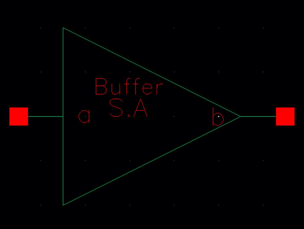
| Buffer Schematics | Buffer Symbol |
| 
|
The
buffer circuit consistes of 6 inverters enough to drive capcitive load.
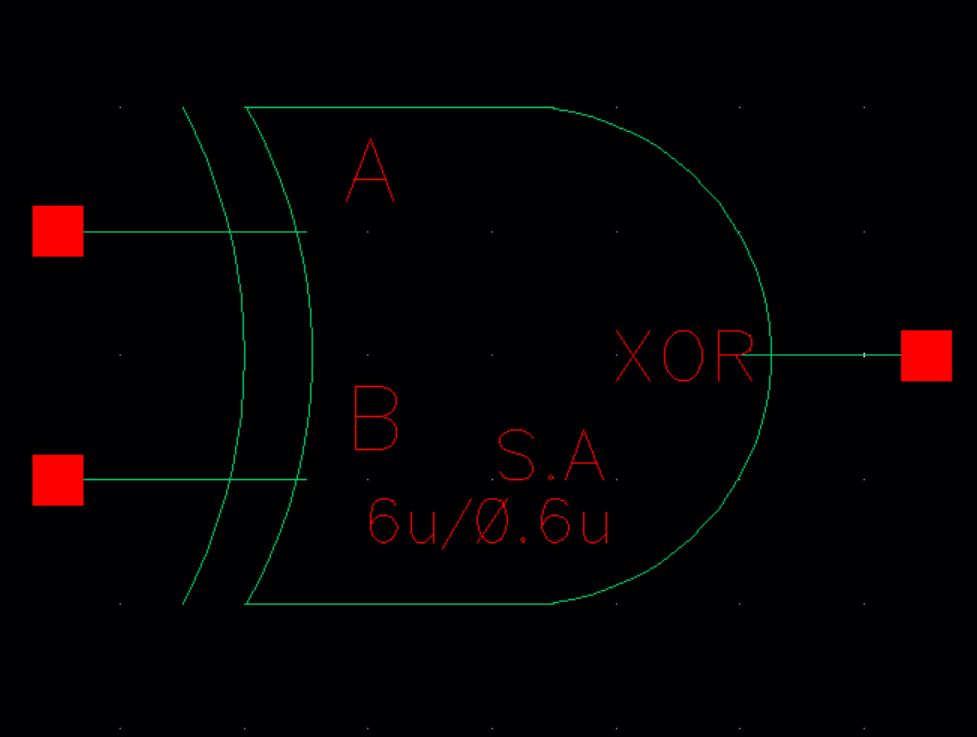
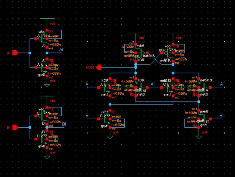
| XOR Schematic | XOR Symbol |

| 
|
The XOR is used to build the even parity generator and the detector.
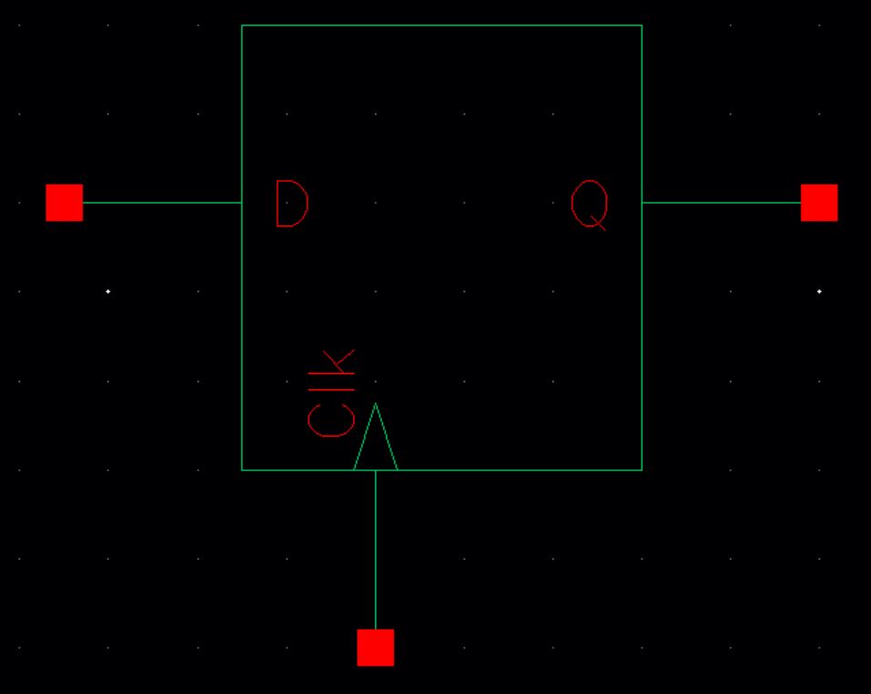
| DFF Schematic | 8-bit NOR Symbol |
| 
|
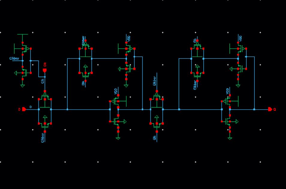
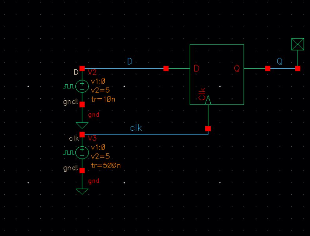
A DFF is used to impliment the serial to parallel converter that is used to loaded the 9-bit word into the Even Parity Checker
| Sim Dff | Sim Dff plot |
| 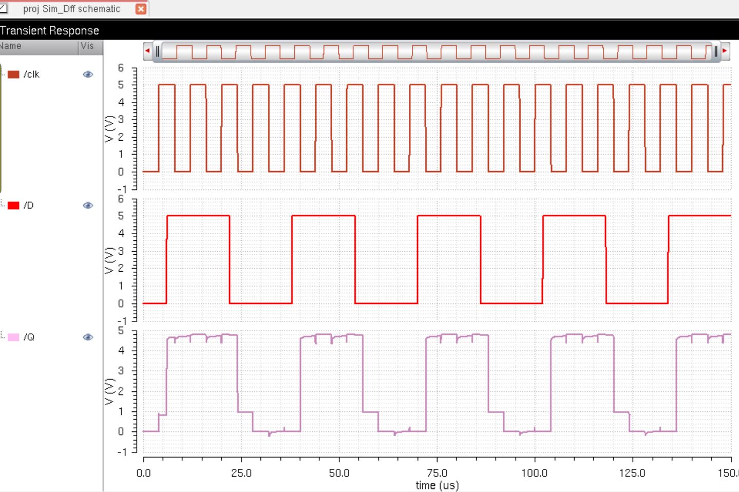
|
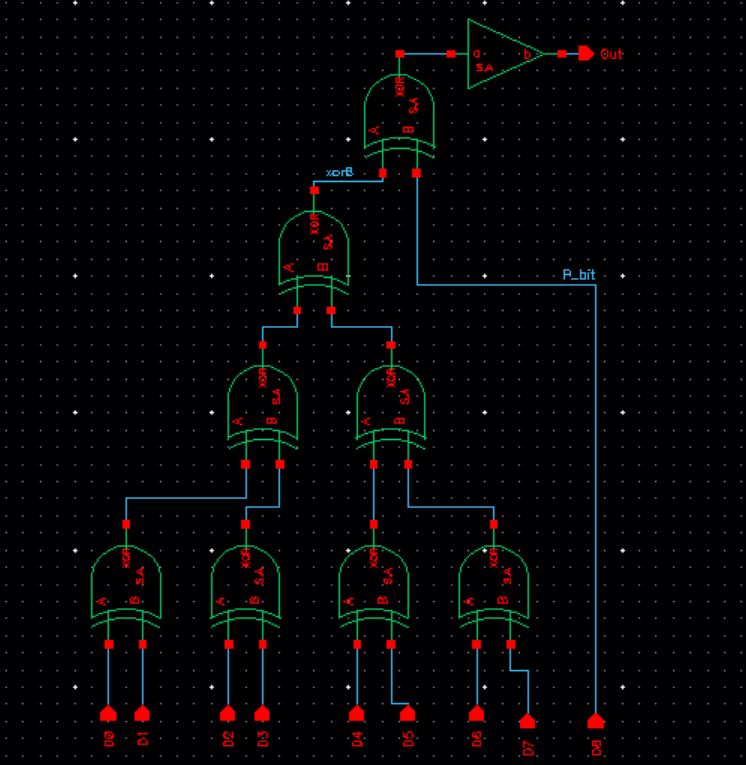
| Even Parity Checker Schematic | Even Parity Checker Symbol |
 | 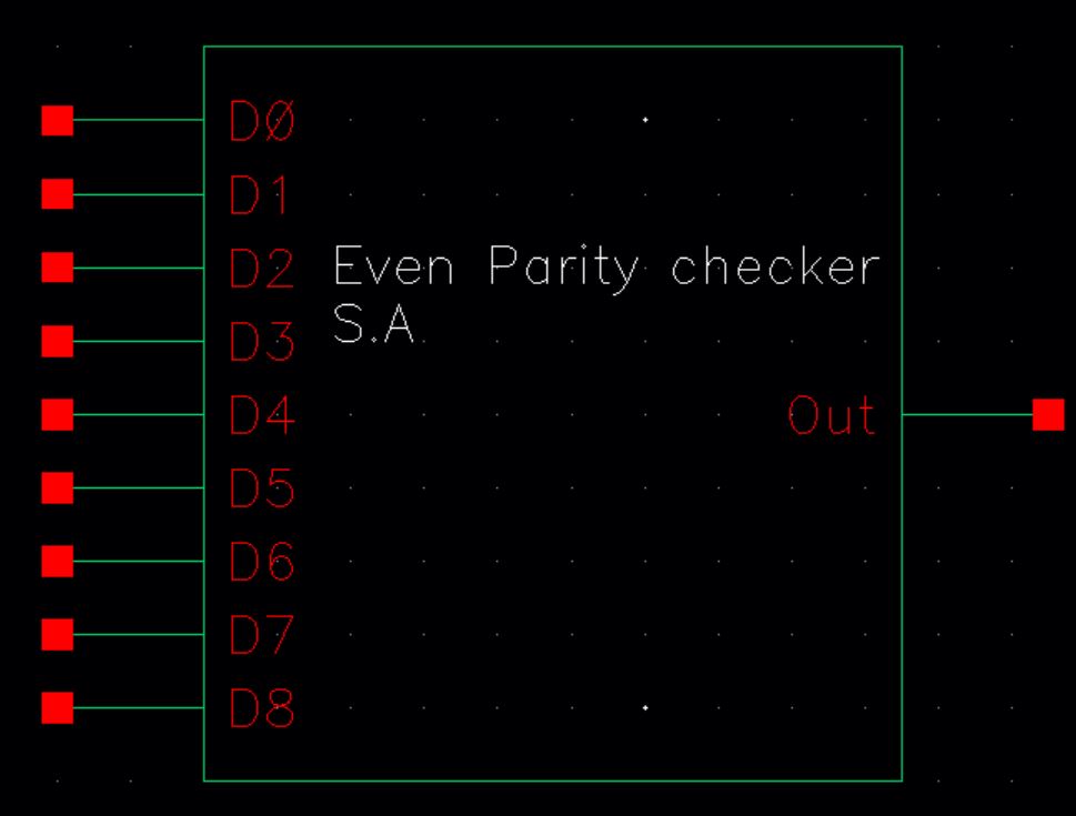 |
The even parity checker schematic consistes of 8 XORs and a Buffer
| Schematic for simulating of Even Parity Checker |
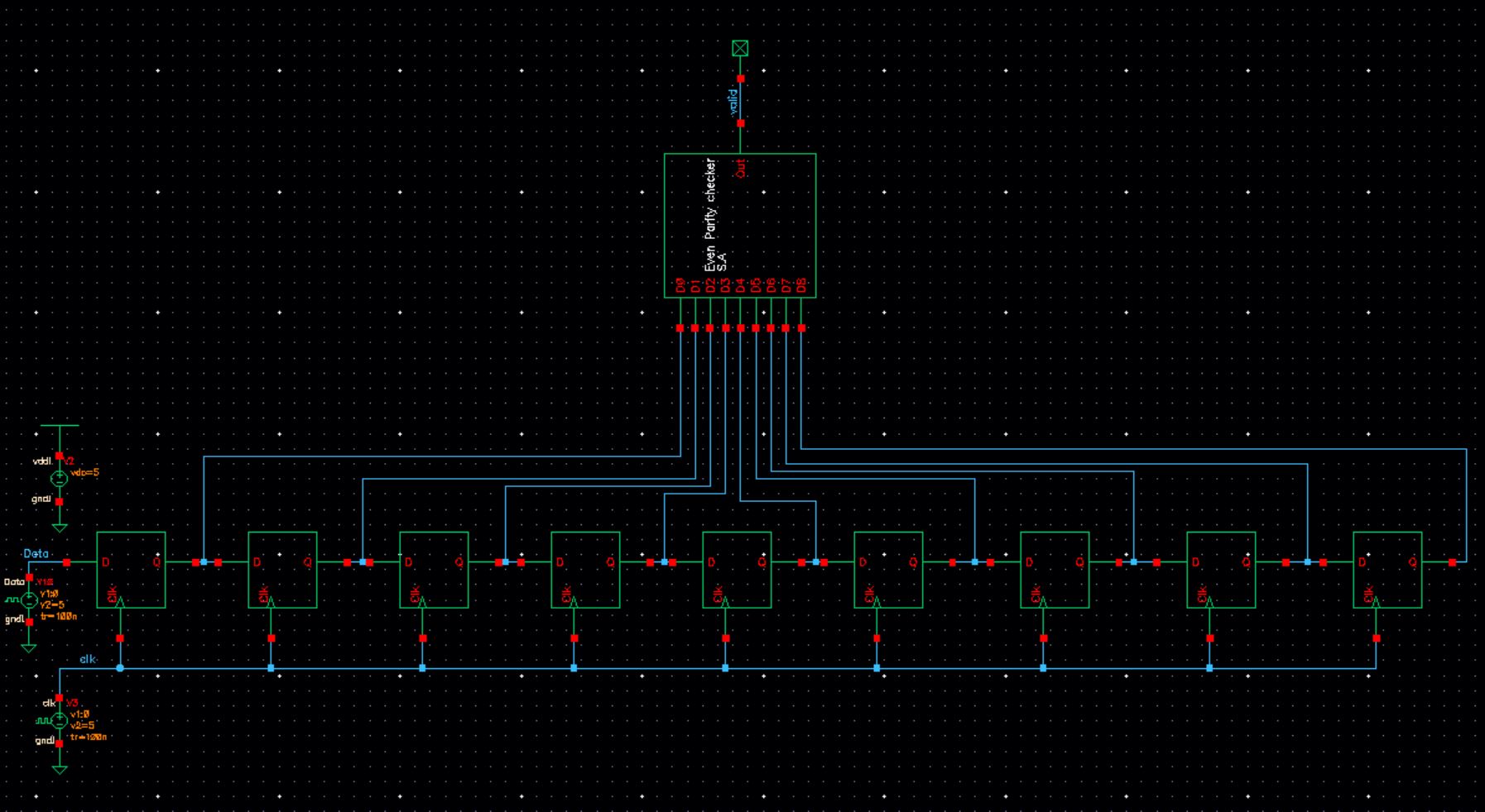 |
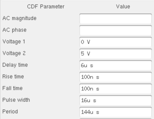
| Clock Vpulse parameters | Data Vpulse parameters |
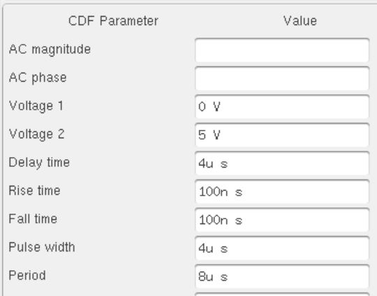 |  |
| The clock speed is set 4 times as faster than data pulse-width which is 60% above the Nyquest sample rate. | logic 1 or 0 = 16us pulse-width thus for 9-bits there are 144us. |
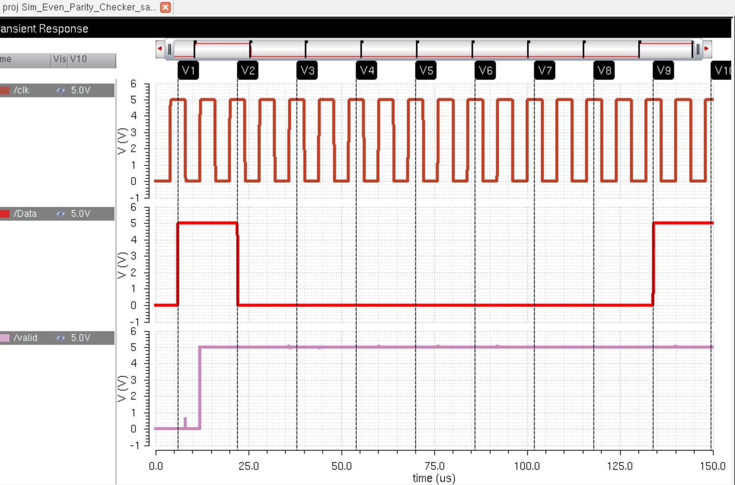
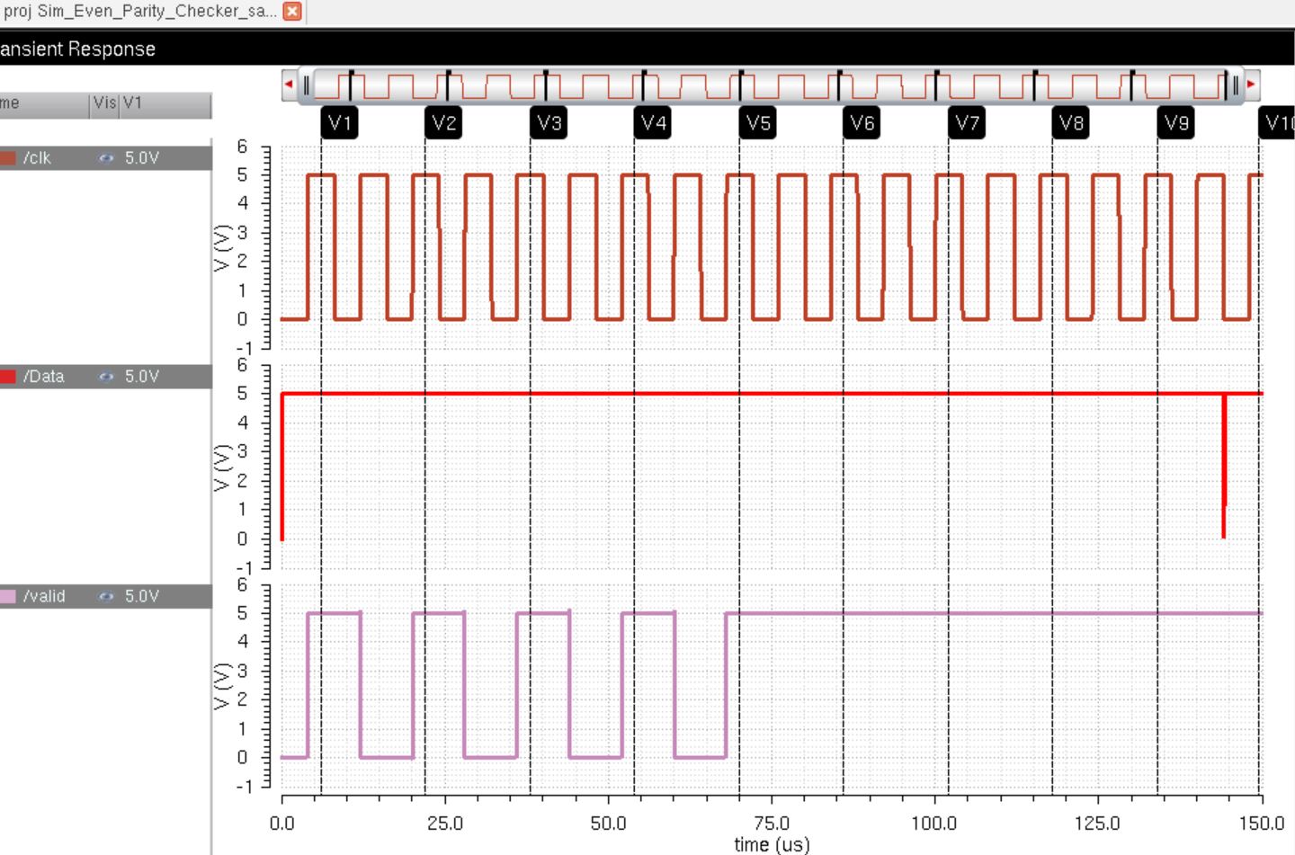
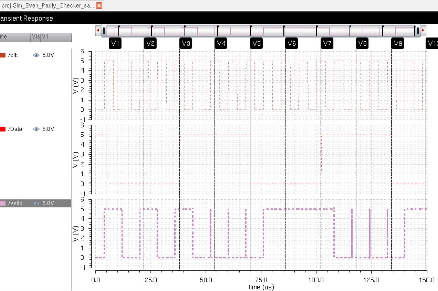
| 9-bit Data input | Valid | Simulation of Even Parity Checker Plot
The validity of this input is indicated at the end of the "Valid" wave form between V9 and V10. |
| 10000000 1 | Yes |  |
| 10000000 0 | No | 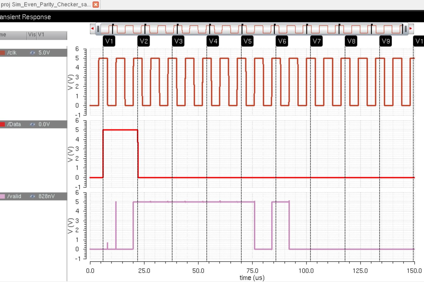
|
| 10101010 1 | Yes | 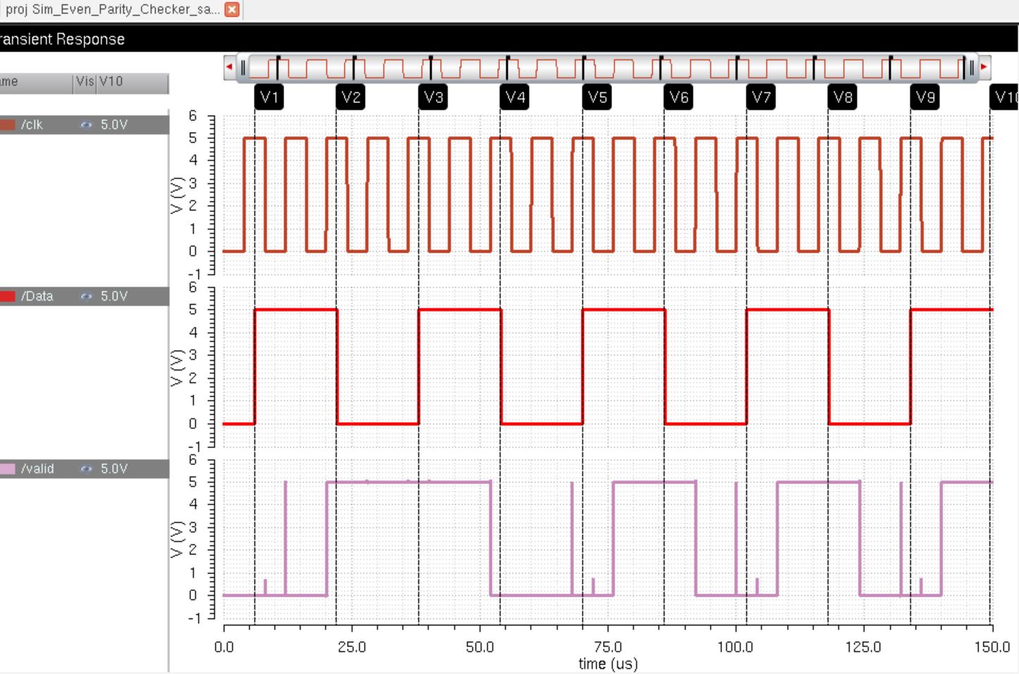 |
| 1111 1111 1 | Yes |  |
| 11100011 1 | Yes | 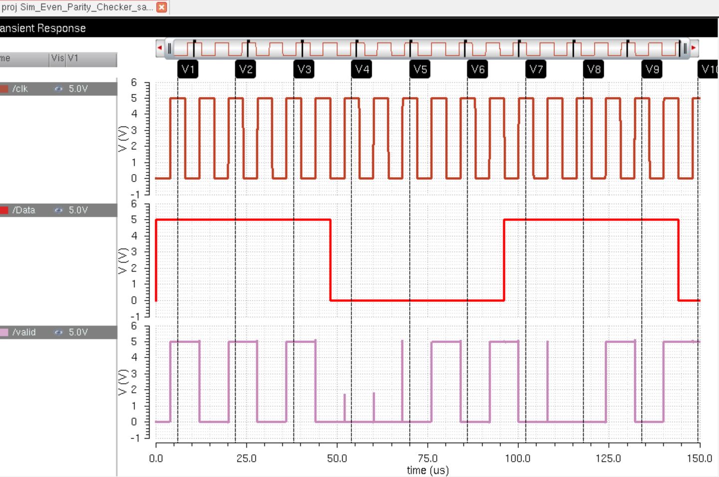 |
| 11110000 1 | No | 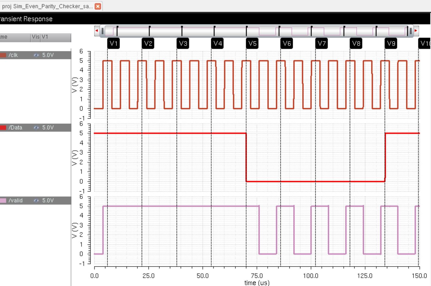 |
| 00110011 0 | Yes |  |
| 00111000 0 | No | 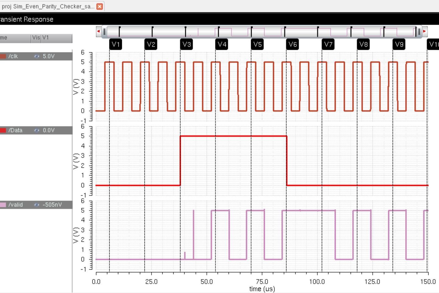 |
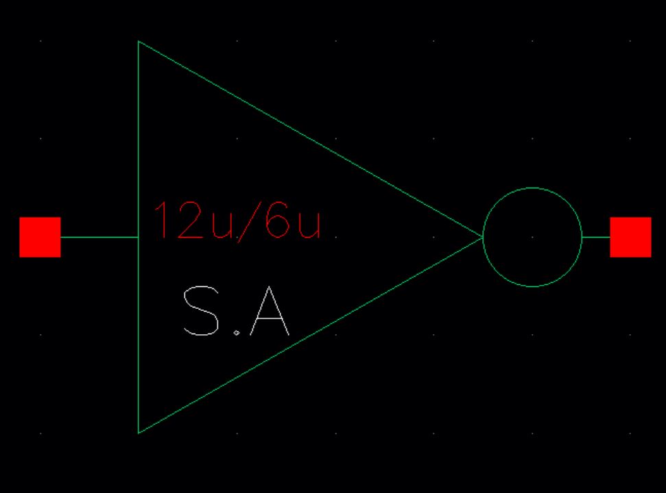
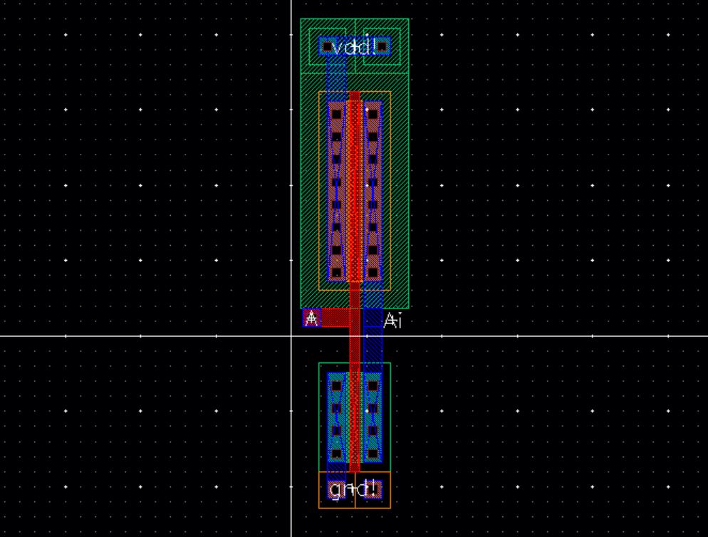
| inverter Schematics | inverter Layout |
|  |
The inverter Layout having 12u/6u is used to implemnt the buffer.
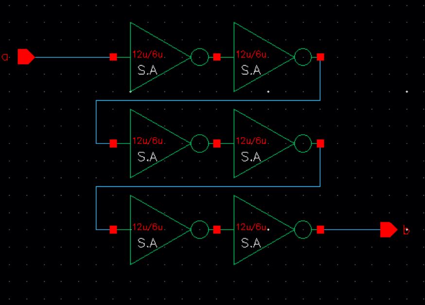
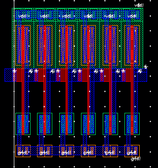
| Buffer Schematics | Buffer Layout |
|  |
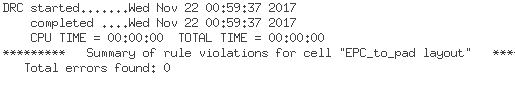
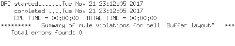
| DRC | LVS |
 | 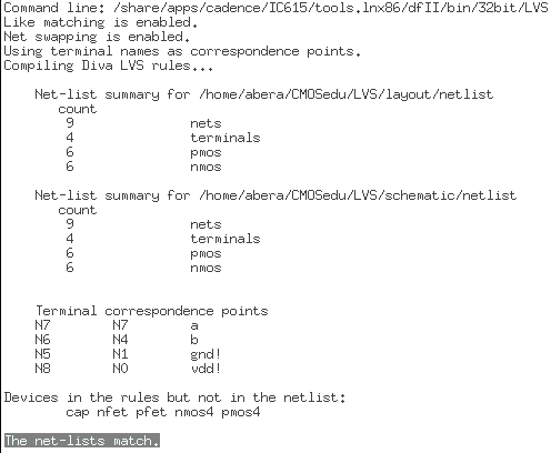 |
The buffer is layed out using 6 inverter and passed DRC and LVS| XOR Schematic | XOR Layout |
|  |
| DRC | LVS |
 | 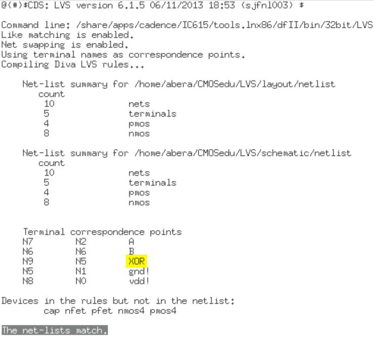 |
The XOR layout with DRC and LVS wchich will be used to make the even parity generator
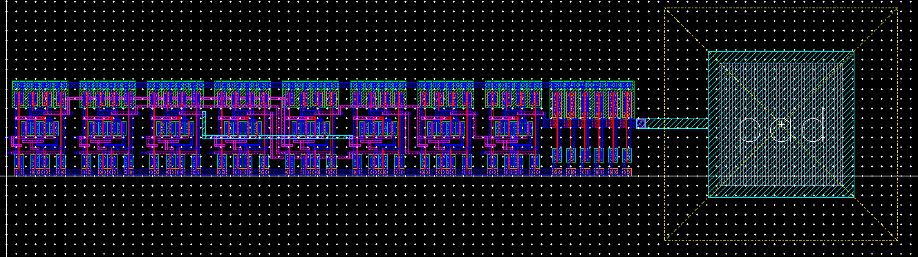
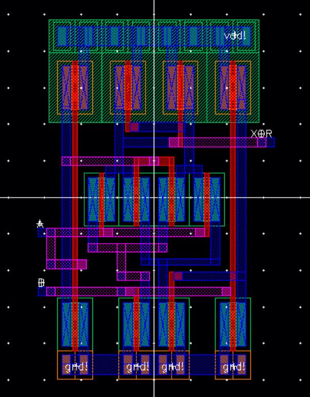
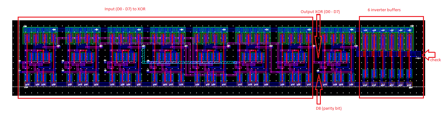
| Even Parity Checker layout |
 |
 |
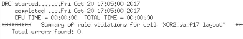
| DRC | LVS |
 |  |
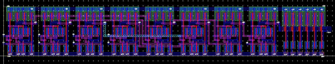
Even
Parity Checker layout on the left and the buffer on the right side of
the layout passed DRC and LVS. The inputs (D0-D7), D8 (parity bit),
and output (check) all have been illustrated in the diagram.
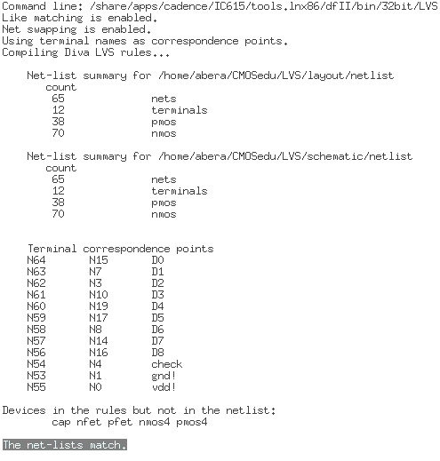
Even Parity Checker schematic and layout connected to a pad
| Schematic | Layout | |
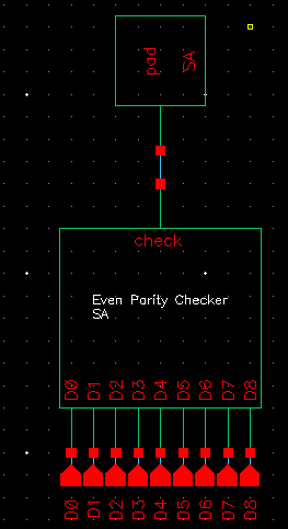 |  | |
Project files
Return to Abera lab
Return to EE 421L Labs


