Lab 2 - EE 421L
Authored
by Surafel Abera
Abera@unlv.nevada.edu
September 13, 2017
Pre-lab work:
I back-up my work on Onedrive
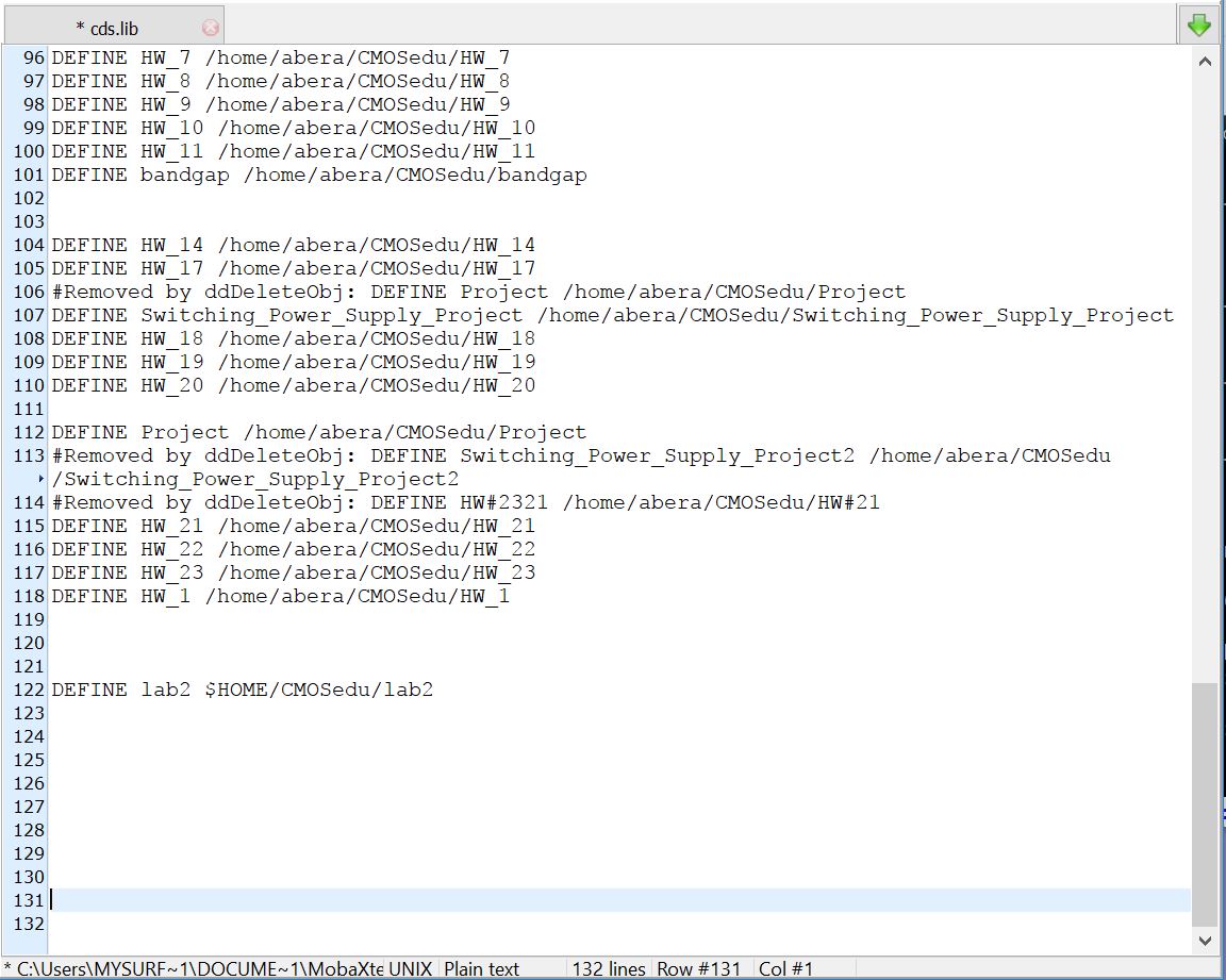
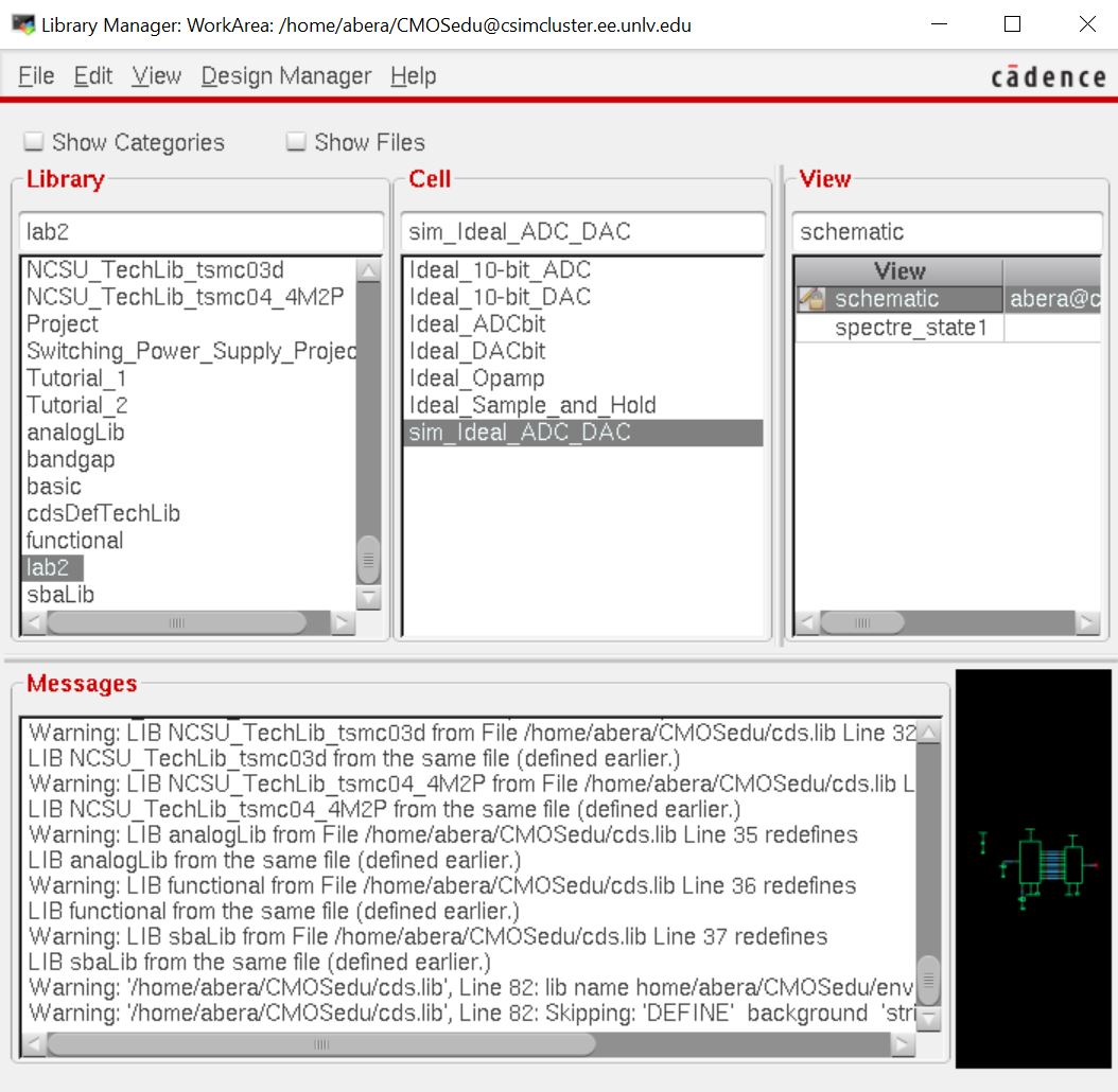
I unzip this directory and added "DEFINE lab2 $HOME/CMOSedu/lab2" to my cds.lib in the design directory.
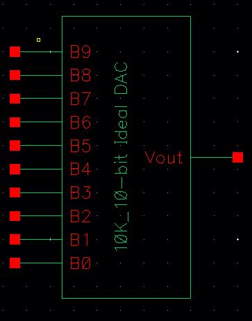
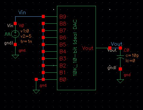
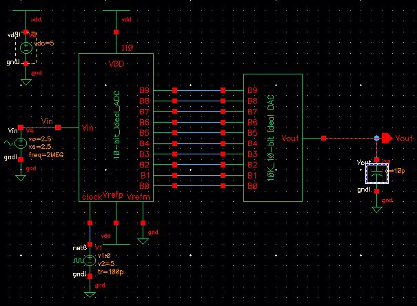
Schematic view of the cell sim_Ideal_ADC_DAC.
Ideal 10-bit ADC and DAC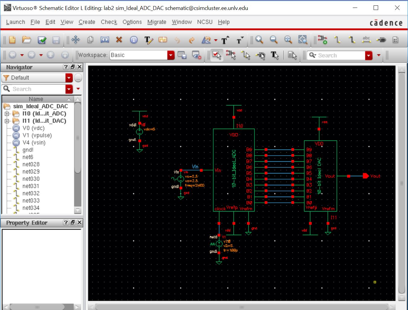
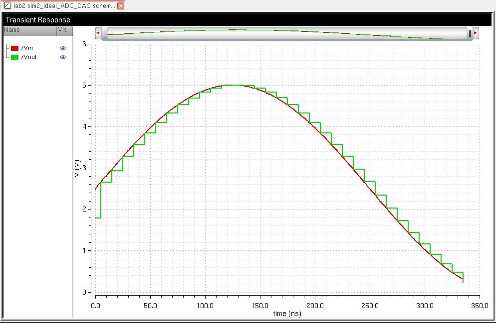
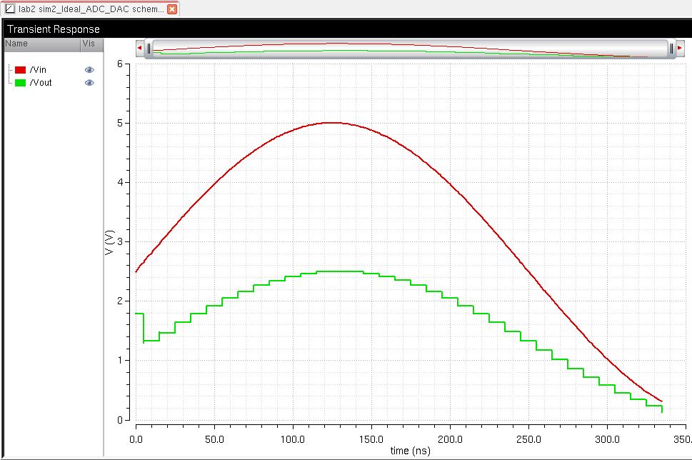
Runing the simulation of Ideal 10-bit ADC and DAC
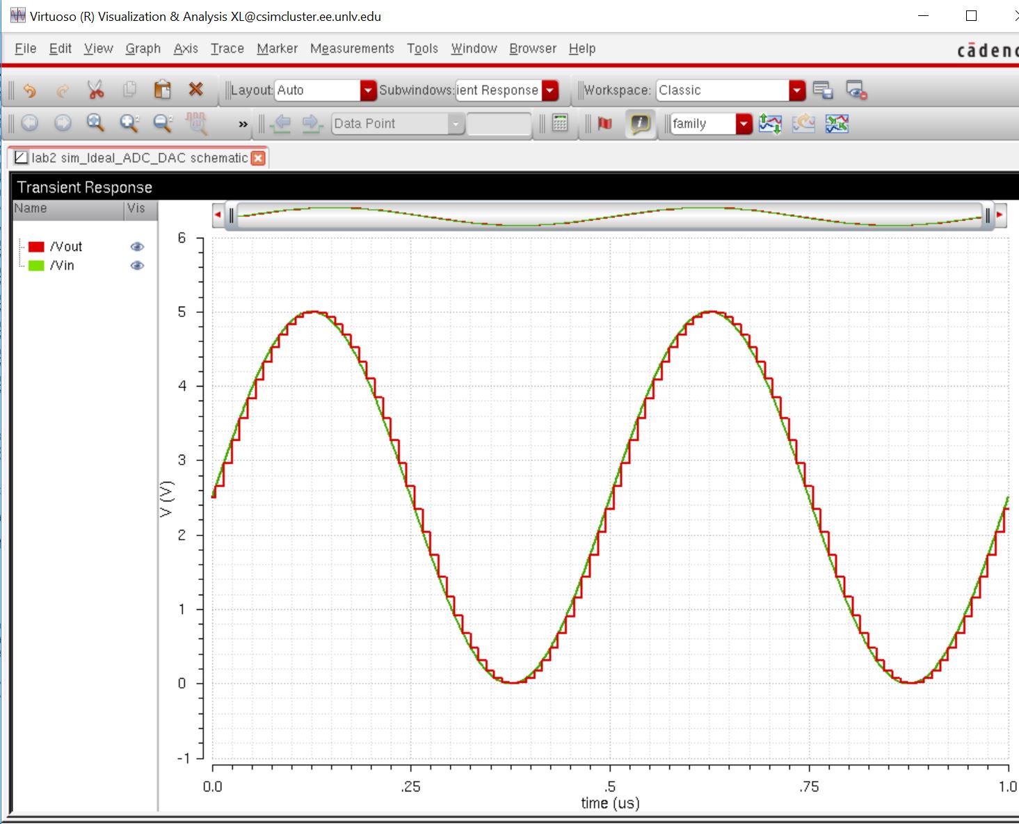
Runing the simulation of Ideal 10-bit ADC and DAC
Frequency
is set to 10MHz
Offset is set to 2.5mV
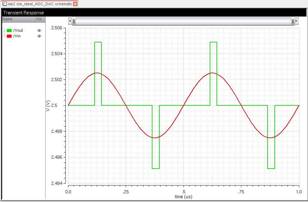
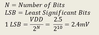
The value of the least
significant bit is calculated using the formula in this lab the
ideal ADC_DAC schematic the VDD is set to 2.5V with 2.5V offset there for 2.5V
is the max amplitude of the signal.
Lab Report Documentation:
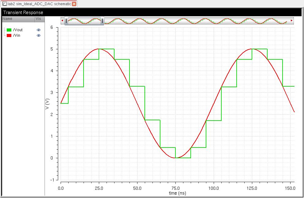
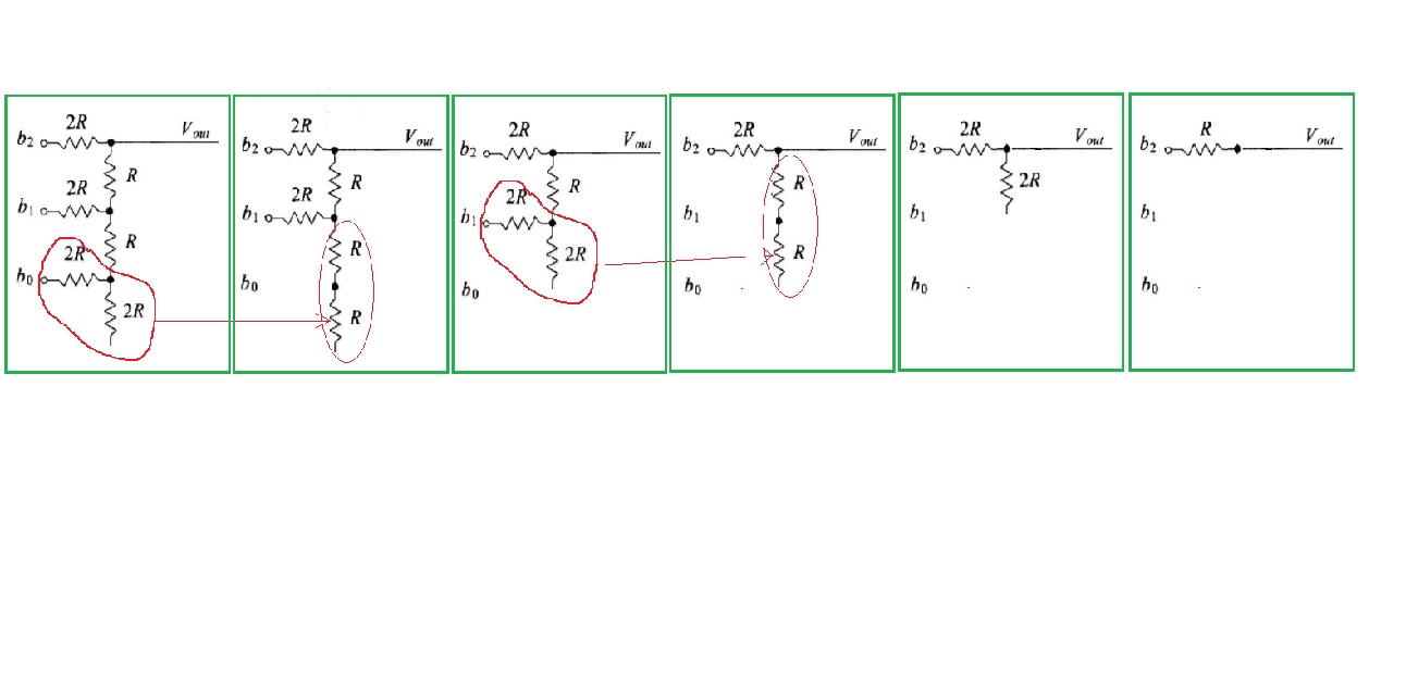
- The
design of a 10-bit DAC using an n-well R of 10k
Once i created a 10 bit DAC using 10K ohm then i created a symbol for it from Cellview.
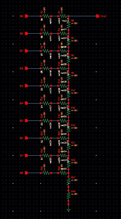
How
to determine the output resistance of the DAC (answer: R) by
combining resistors in parallel and series
The value of the least
significant bit is calculated using the formula VDD/2^N. In this lab the
ideal ADC_DAC schematic the VDD is set to 2.5V with 2.5V offset there for 2.5V
is the max amplitude of the signal.
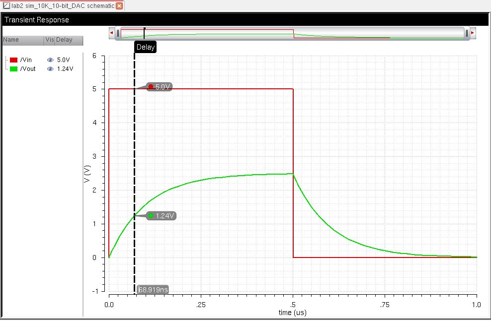
Delay, Driving a Load
- Ground
all DAC inputs except B9. Connect B9 to a pulse source (0 to VDD) and
show, and predict using 0.7RC, the delay the DAC has driving a 10 pF load
Using the delay time formula Td= 0.7RC = 0.7(10K)(10p)=70ns
- Simulations
to verify the design functions correctly.
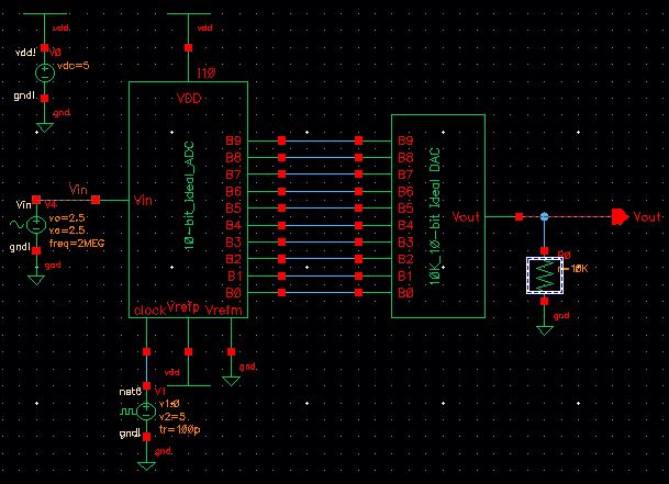
First i copied
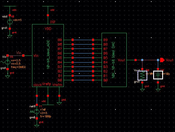
the schematic cell view sim_Ideal_ADC_DAC to a cell sim2_Ideal_ADC_DAC
and replaced the ideal DAC with the one i just designed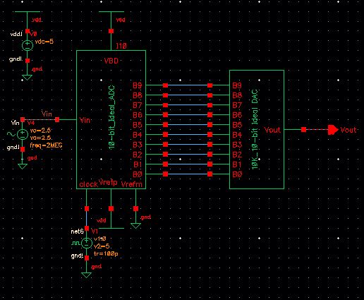
- The designed DAC drives a load R = 10K ohm
The 10K ohm load adds to the circuits resistance and
acts as a voltage divider there for the output voltage is cut by half.
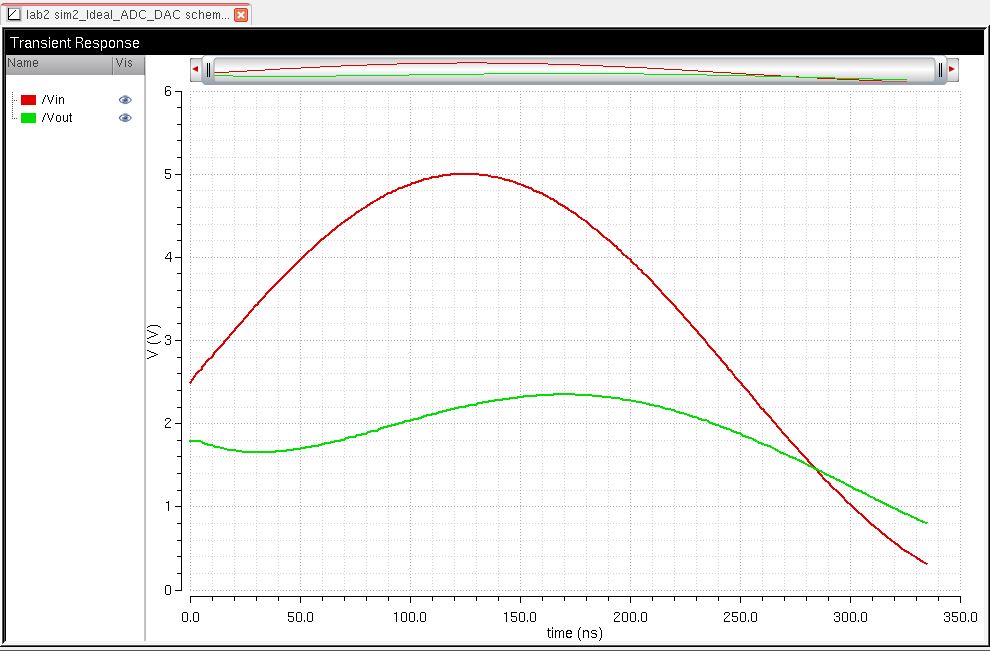
- The designed DAC drives capacitiv load of 10pF
Adding the capacitor smooths out the output voltage,
adds a delay, and decrease the output voltage.
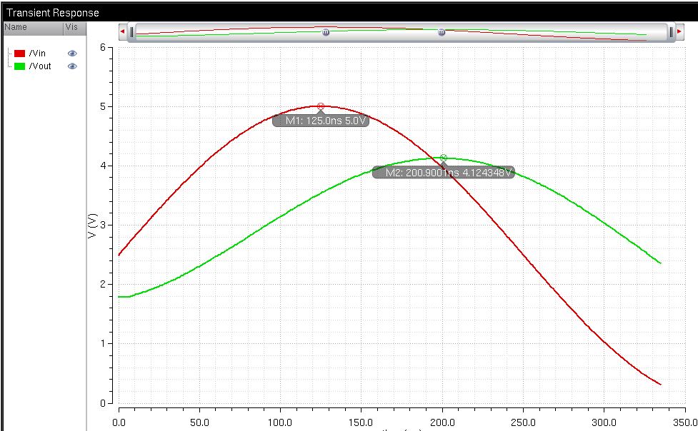
- The designed DAC drives resistive load of R/C
Adding RC in parallel affects the amplitude and adds a delay to the output.
Explain
what happens if the DAC drives a 10k load?
A 10K load would cut the output voltage in half becouse the circuit and the load act as a voltage divider.
 Discuss what happens if the resistance of the switches isn't small compared to R.
If the resistance of the switches
isn't small compared to R, then it would add its resistance to R and
creates undesired effects on the Voltage output.
Return to lab2
Return to EE 421L Labs