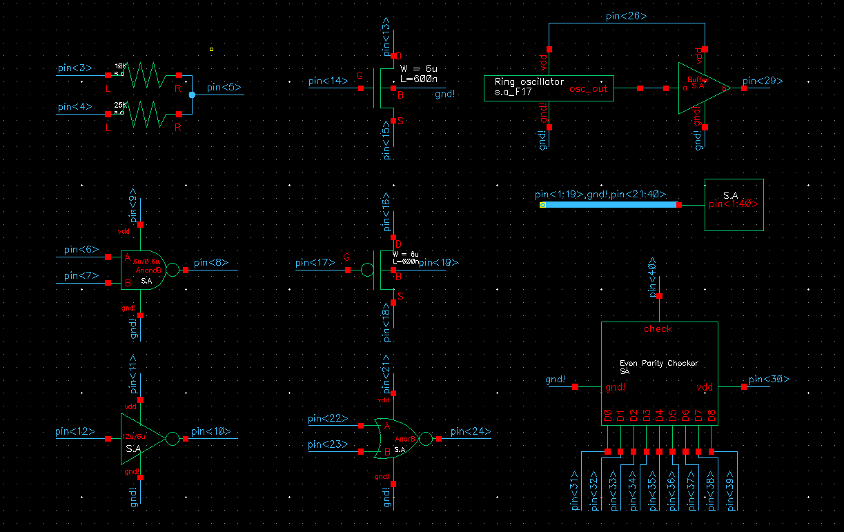
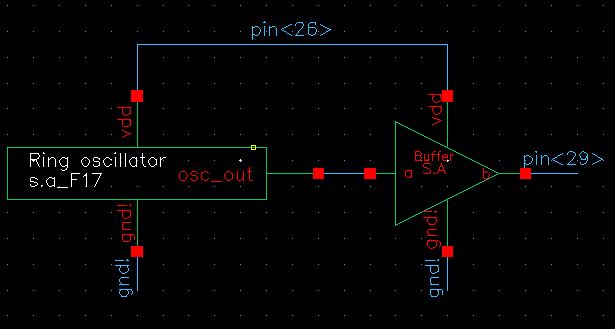
A 31-stage ring oscillator with a buffer for driving a 20 pF off-chip load
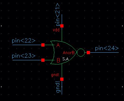
NAND and NOR gates using 6/0.6 NMOSs and PMOSs
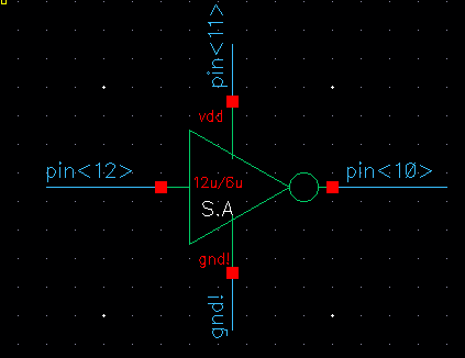
An inverter made with a 6/0.6 NMOS and a 12/0.6 PMOS
Transistors,
both PMOS and NMOS, measuring 6u/0.6u where all 4 terminals of each
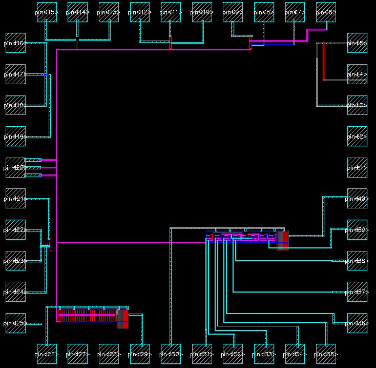
device are connected to bond pads (7 pads + common gnd pad)
Note
that only one pad is needed for the common gnd pad. This pad is used to
ground the p-substrate and provide ground to each test circuit
Using
the 25k resistor laid out below and a 10k resistor implement a voltage
divider (need only 1 more pad above the ones used for the 25k
resistor)
A 25k resistor implemented using the n-well(connect between 2 pads but we also need a common gnd pad)
Whatever else you would like to fabricate to use the remaining pins on the chip
Feel free to "sign" the chip or add a graphic (see the bottom of thiswebpage). Copy the final, DRC and LVS clean cell you want to fabricate, and then add the graphic since the graphic won't DRC
Also
note that you can reduce the number of pins needed by sharing some
of them (two resistors, for example, only need 3 pins)