| Lab work Back-up | Tutorial 2 completed |
 |  |
Lab 4 - EE 421L
| Lab work Back-up | Tutorial 2 completed |
| |
Schematics and simulations of NMOS
| Schematics NMOS size: 6u/600n width-to-length ratio | Simulation |
 | 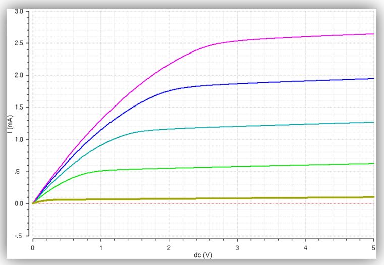 |
| ID v. VDS of an NMOS device for VGS varying from 0 to 5 V in 1 V steps while VDS varies from 0 to 5 V in 1 mV steps. | |
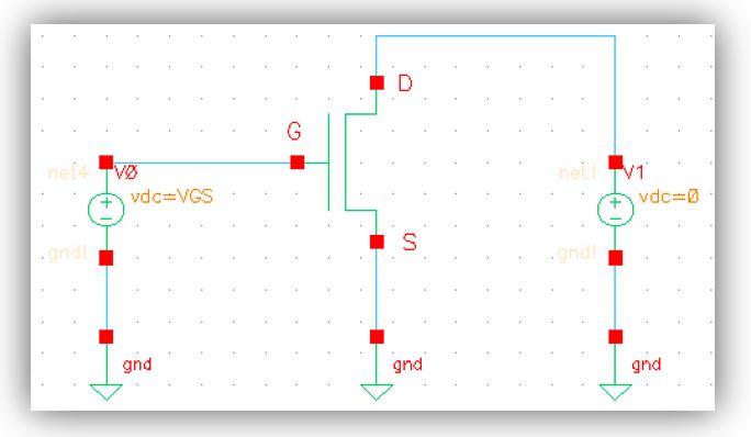
| Schematics NMOS size: 6u/600n width-to-length ratio | Simulation |
 | 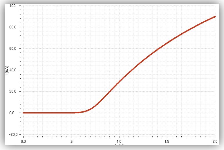 |
| ID v. VGS of an NMOS device for VDS = 100 mV where VGS varies from 0 to
2 V in 1 mV steps. | |
Schematics and simulations of PMOS
| Schematics PMOS size: 12u/600n width-to-length ratio. | Simulation |
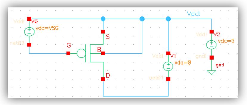 | 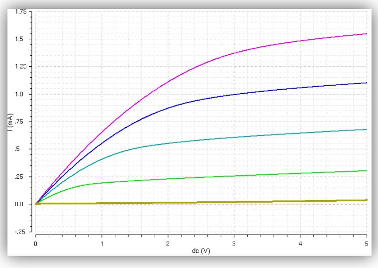 |
| ID v. VSD of a PMOS device for VSG varying from 0 to 5 V in 1 V steps while VSD varies from 0 to 5 V in 1 mV steps. | |
| Schematics PMOS size: 12u/600n width-to-length ratio. | Simulation |
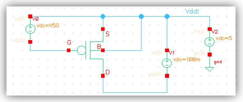 | 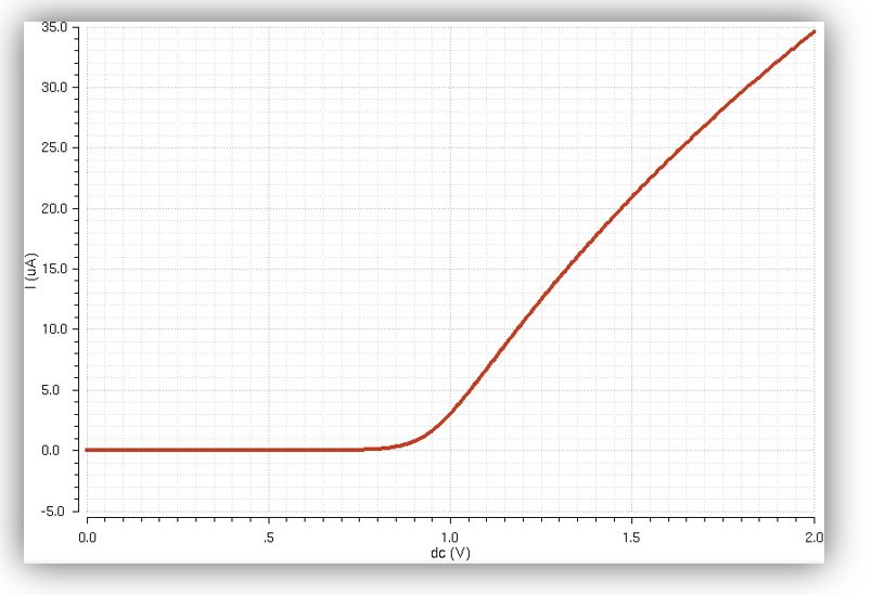 |
| ID v. VSG of a PMOS device for VSD = 100 mV where VSG varies from 0 to 2 V in 1 mV steps. | |
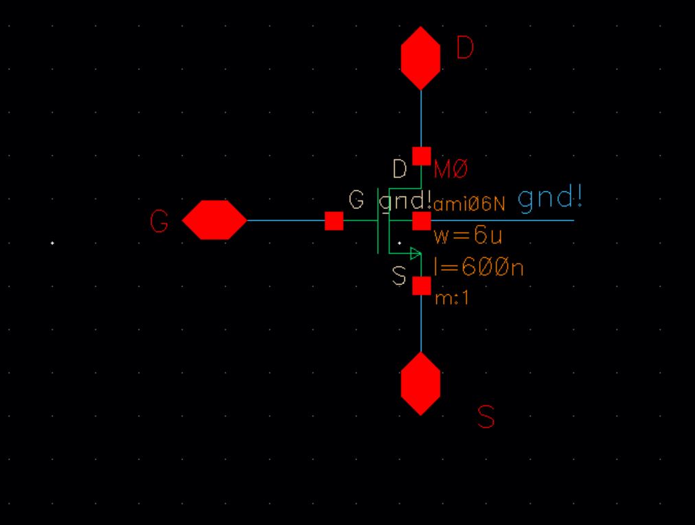
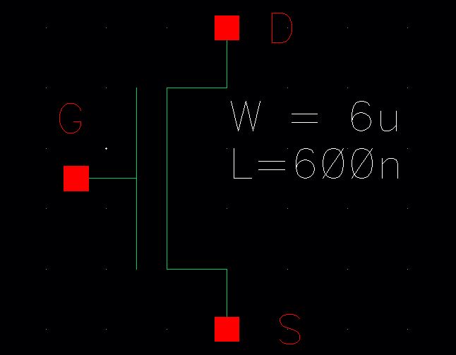
Layout of a 6u/0.6u NMOS
| Schematic | Symbol | LVS |
 |  |  |
| Layout | Extracted | DRC |
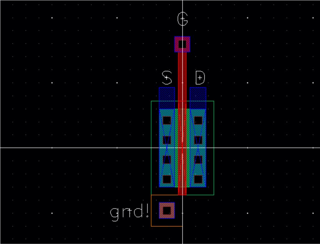 | 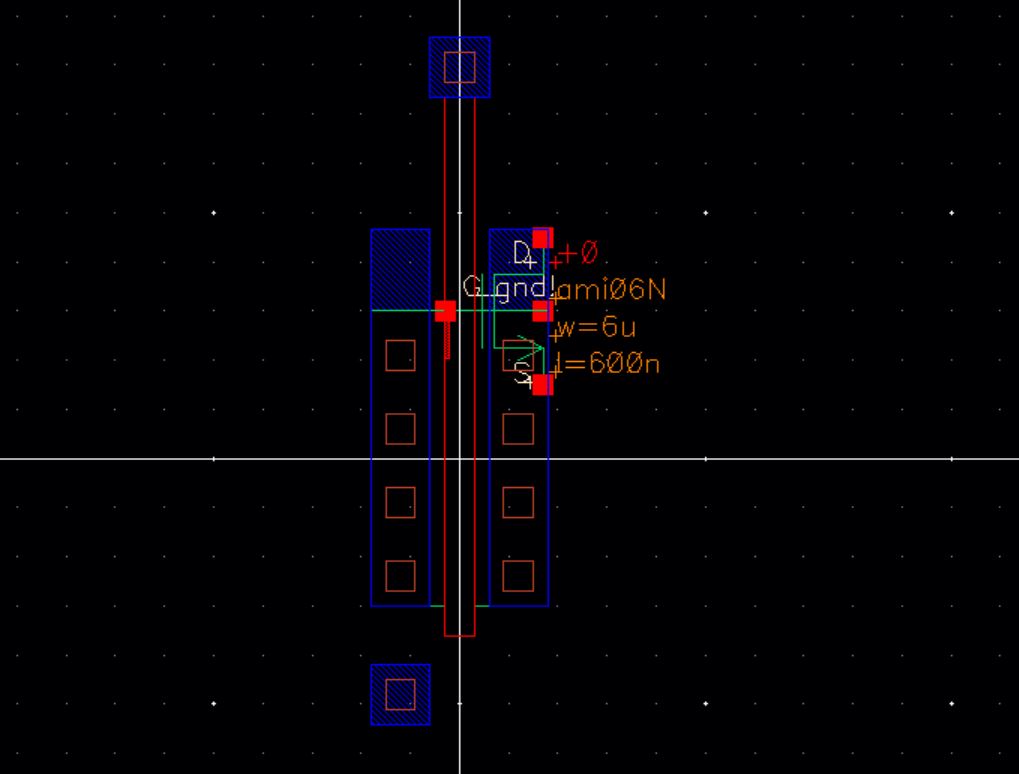 | 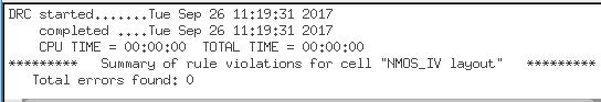 |
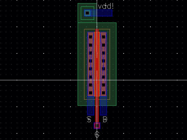
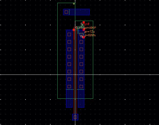
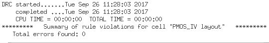
Layout of a 12u/0.6u PMOS
| Schematic | Symbol | LVS |
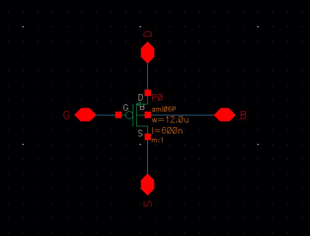 | 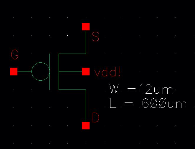 | 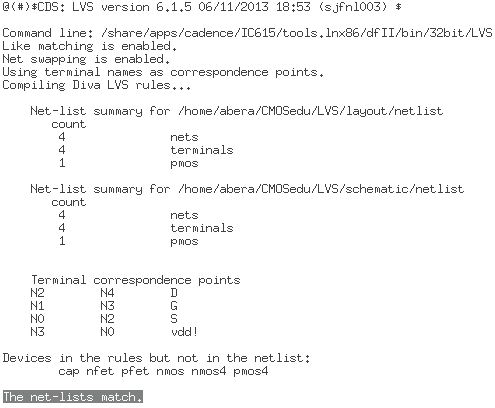 |
| Layout | Extracted | DRC |
 |  |  |
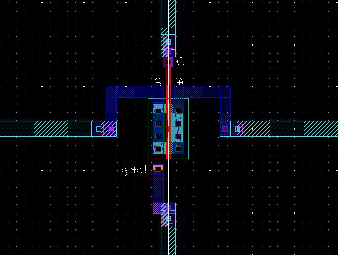
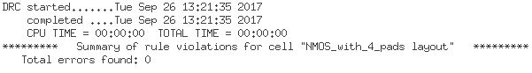
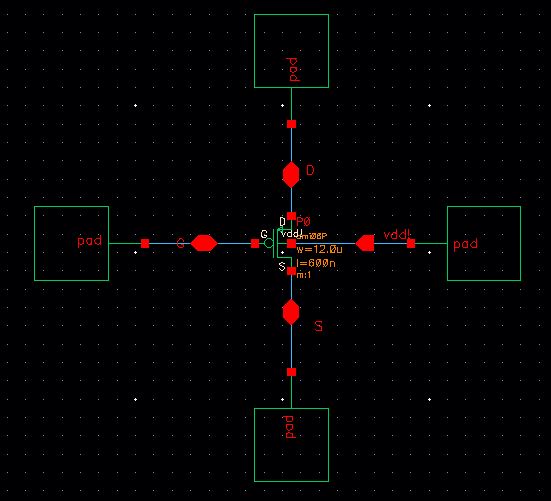
Layout of a 6u/0.6u NMOS connected to 4 probe Pads
| 4 Pad NMOS Schematic | Closeup of Extracted NMOS with Pad | LVS |
 | 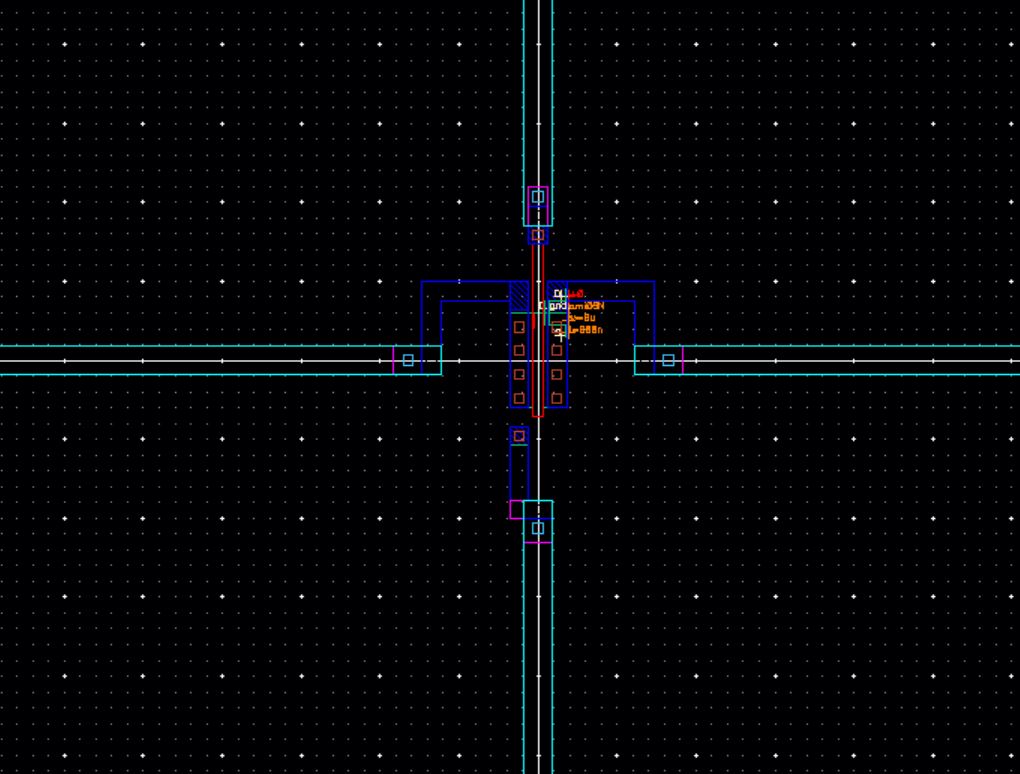 |  |
| Layout NMOS with Pad | Closeup of Layout NMOS with Pad | DRC |
 |  |  |
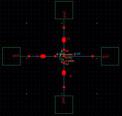
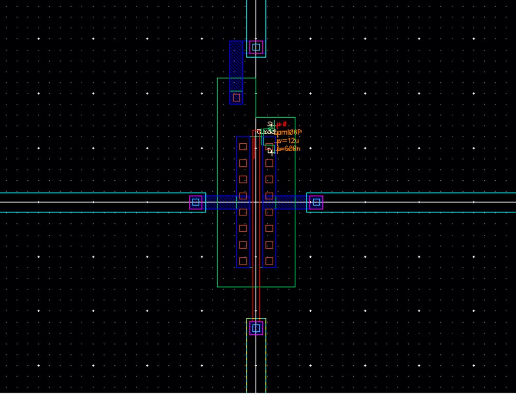
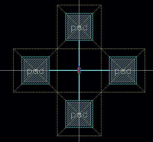
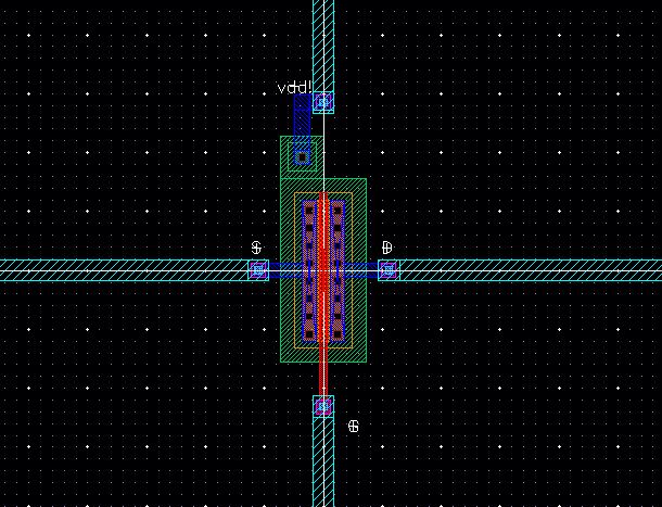
Layout of a 12u/0.6u PMOS connected to 4 probe Pads
| 4 Pad NMOS Schematic | Closeup of Extracted NMOS with Pad | LVS |
 |  |  |
| Layout NMOS with Pad | Closeup of Layout NMOS with Pad | DRC |
 |  | 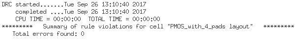 |