| Lab work Back-up | Tutorial 5 completed |
 |  |
Lab 7 - EE 421L
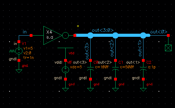
The 4-bit inverter is drafted in a concise manner having 4 inverters for 4 bits input 4 bits outpus. A symbole is created representing a 4-bit inveter with X4.
| Simulation 4-bit inverter | 4-bit inverter Plot |
 | 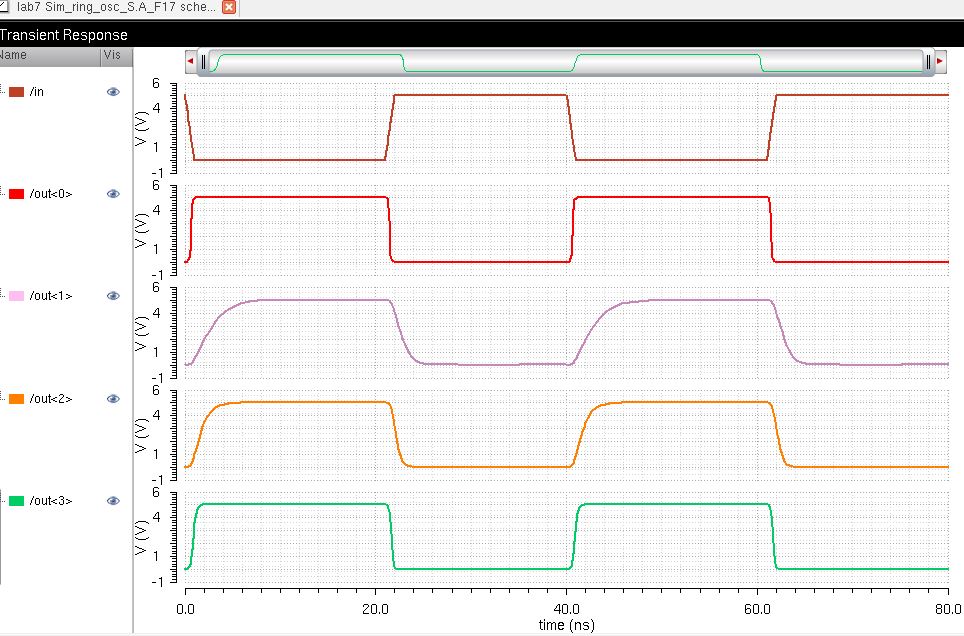 |
The 4-bit inveter driving 3 diffrent size capacitors inorder to analyse the performance of the inverters. The plot show the inverter performed best when driving 100fF capcitor on out<3> .
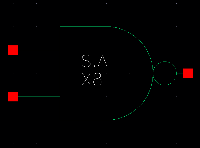
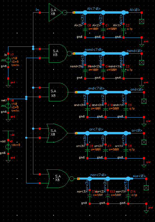
Schematic and Symbol for 8-bit input/output array of:NAND, NOR, AND, inverter, and OR
| 8-bit NAND Schematic | 8-bit NAND Symbol |
 |  |
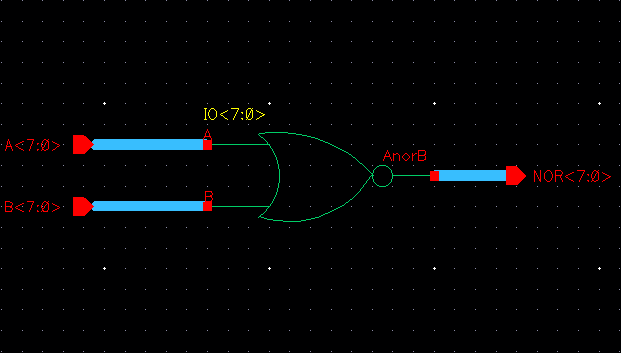
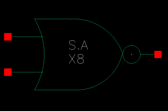
| 8-bit NOR Schematic | 8-bit NOR Symbol |
 |  |
| 8-bit AND Schematic | 8-bit AND Symbol |
 |  |
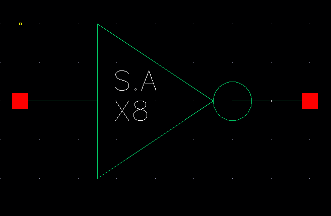
| 8-bit Inverter Schematic | 8-bit Inverter Symbol |
 |  |
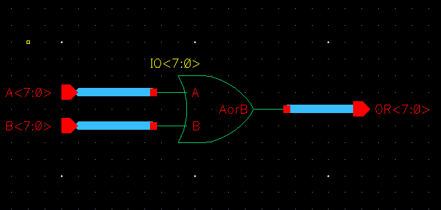
| 8-bit OR Schematic | 8-bit OR Symbol |
 |  |
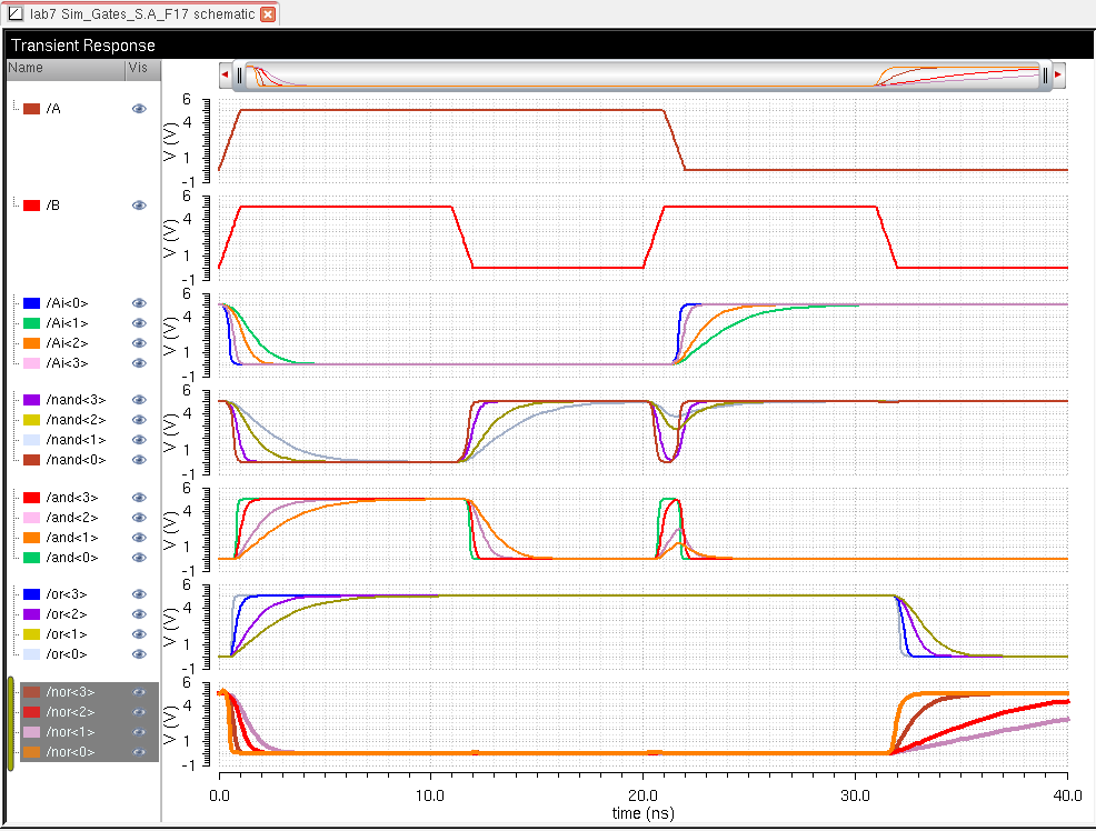
| 8-bit Gates Schematic | 8-bit Gates Plots |
 |  |
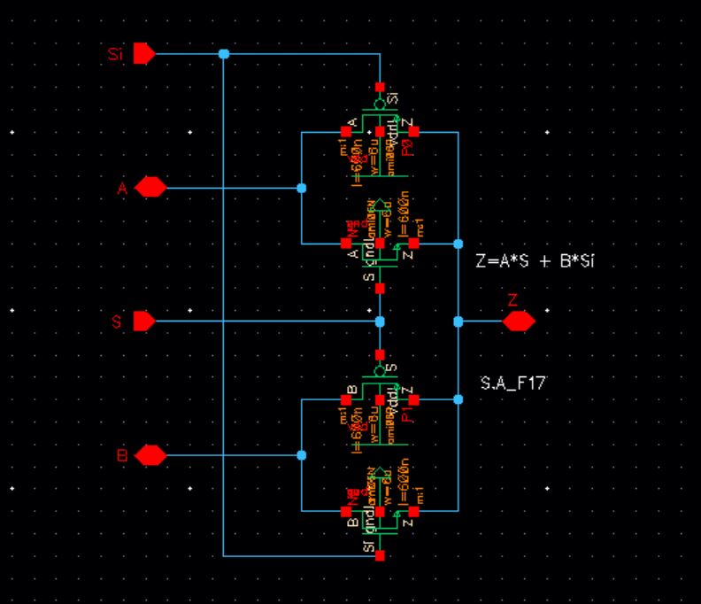
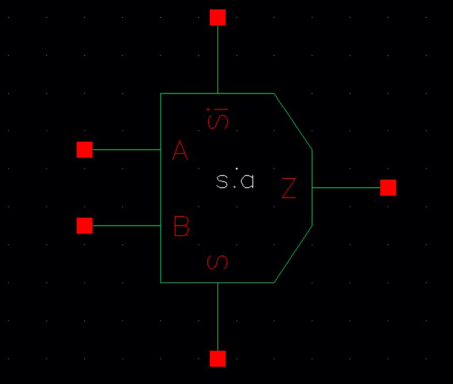
| 2-to-1 MUX Schematic | 2-to-1 MUX Symbol |
 |  |
| 2-to-1 MUX Schematic | 2-to-1 MUX Plots |
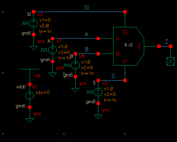 |  |
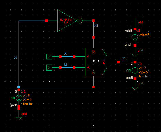
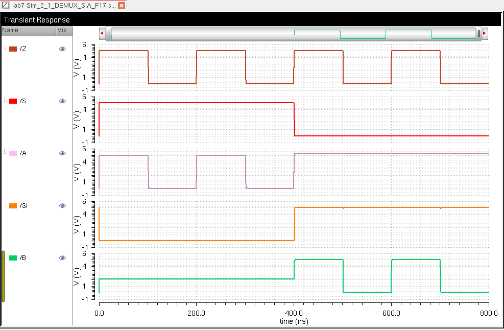
| 2-to-1 DEMUX Schematic | 2-to-1 DEMUX Plots |
 |  |
| 8-bit 2-to-1 MUX/DEMUX Schematic | 8-bit 2-to-1 MUX/DEMUX Symbol |
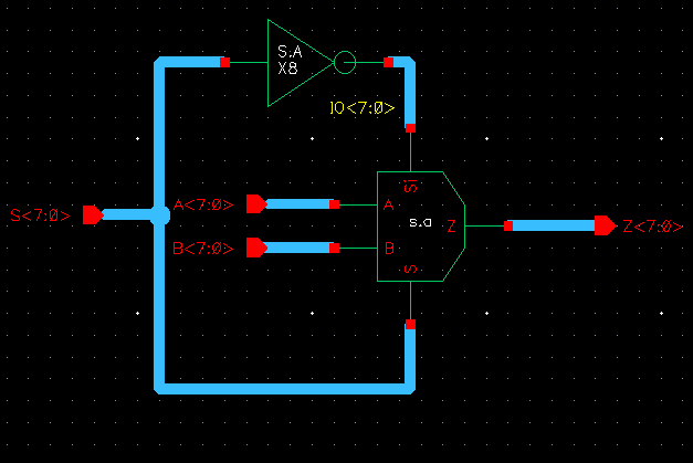 | 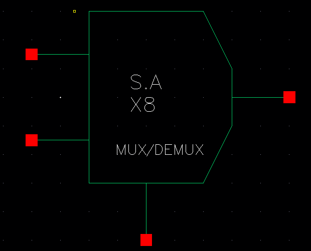 |
After the MUX/DEMUX Schematic verified it is extended to 8-bit 2-to-1 MUX/DEMUX and a symbol is made for it.
| Simulation 8-bit 2-to-1 MUX/DEMUX | Plot 8-bit 2-to-1 MUX/DEMUX |
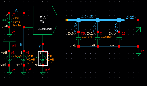 | 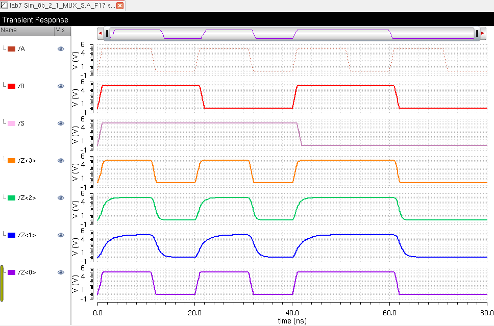 |
The 8-bit Mux/DEMUX is then simulated using three Vpulse for the inputs A, B and S. The output drives three diffrent size capacitors to analayse performance.
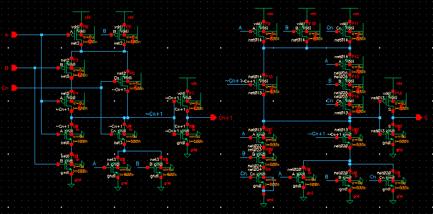
| Full-Adder Schematic | Full-Adder Symbol |
 | 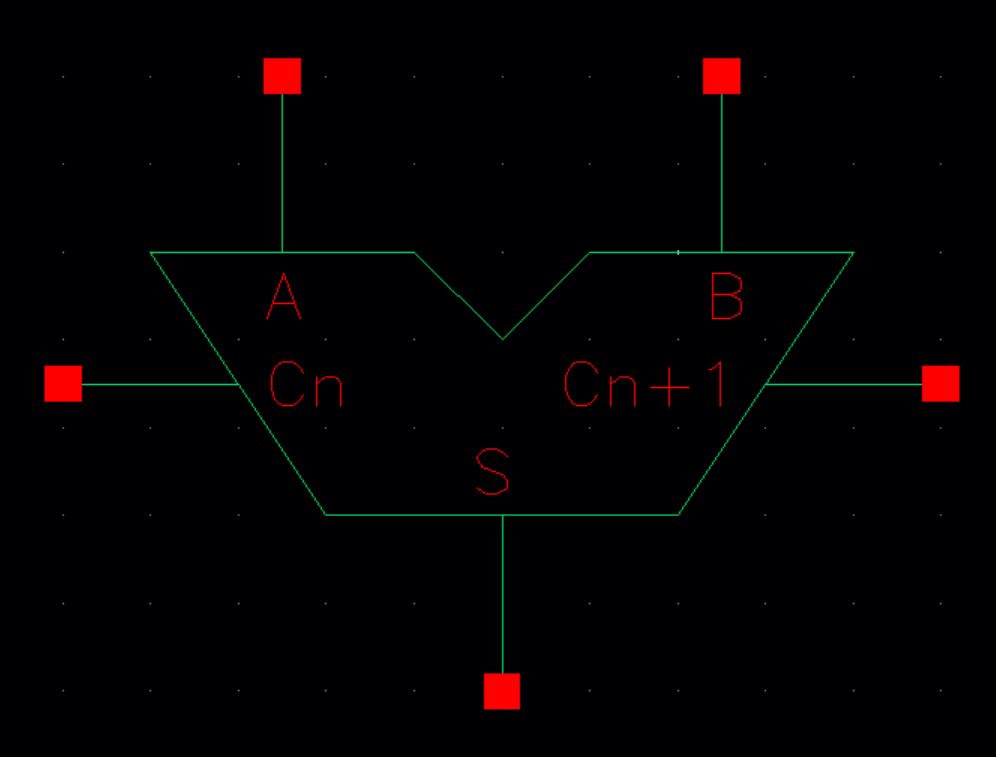 |
| 8-bit Full-Adder Schematic | 8-bit Full-Adder Symbol |
 | 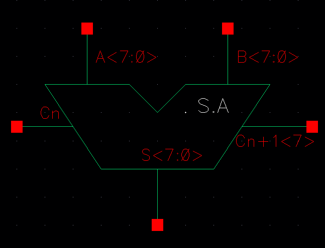 |
The two input full-adder has been extended to 8-bit with two inputs.
| 8-bit Full-Adder Schematic | Plot 8-bit Full-Adder |
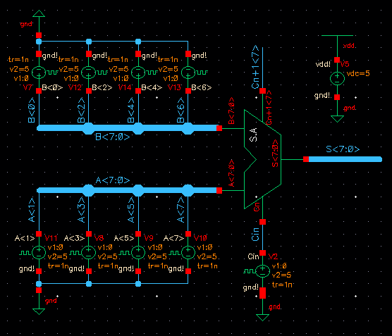 |  |
The full adder circuit is simulated by using 4-bits out of the 8-bits inorder to analyse the performance of the Full-Adder ciruit. 4-bits are sent through input A and 4-bits through B and thier sum is obserbed on the plot "S".
| 8-bit Full-Adder Layout | DRC |
DRC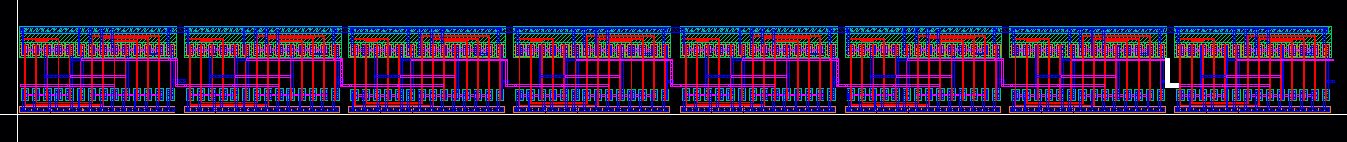 | 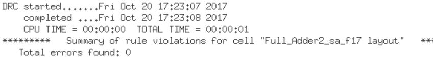 |
| 8-bit Full-Adder Extracted | LVS |
 | 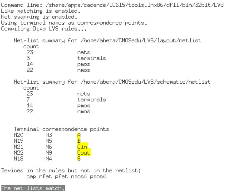 |