Lab 6 - EE 421L 

Authored by Surafel Abera

Abera@unlv.nevada.edu

October 25, 2017


Pre-lab work: 

Lab work Back-upTutorial 4 completed
http://cmosedu.com/jbaker/courses/ee421L/f17/students/abera/lab6/backup_lab6.JPG
http://cmosedu.com/jbaker/courses/ee421L/f17/students/abera/lab6/Tutorial%204.JPG


 Lab Work:
  Draft a schematic and layout for a full adder using NAND and XOR gates


                                2-Input NAND and XOR gate Schematics

 6u/0.6u NAND6u/0.6 XOR
http://cmosedu.com/jbaker/courses/ee421L/f17/students/abera/lab6/NAND/nand_Schematic.JPG
http://cmosedu.com/jbaker/courses/ee421L/f17/students/abera/lab6/XOR/xor_Schematic.JPG
The realization of NAND and XOR gates were first started by drafting the schematics seen above.  The symbols of
each circuit is created inorder to impleament the gates for the rest of the lab and for future lab projects.
   
 NAND SymbolXOR Symbol
http://cmosedu.com/jbaker/courses/ee421L/f17/students/abera/lab6/XOR/xor_Symbol.JPG

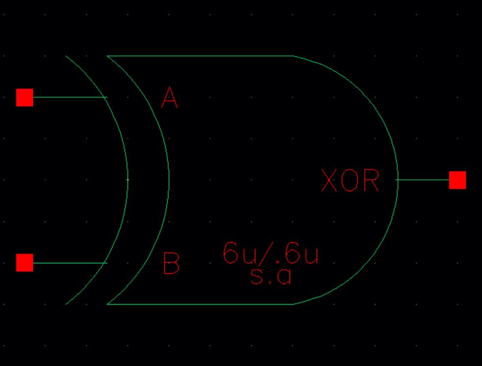
The symbols above have the shape of the corresponding gate function.  The NAND and XOR symbols each contain circuit that will function as their logical symbol represents.   Next the functionality of the gates is checked by simulating the inputs and outputs of the gates using the truth table as a reference.


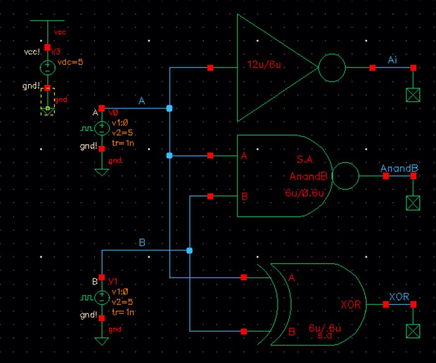
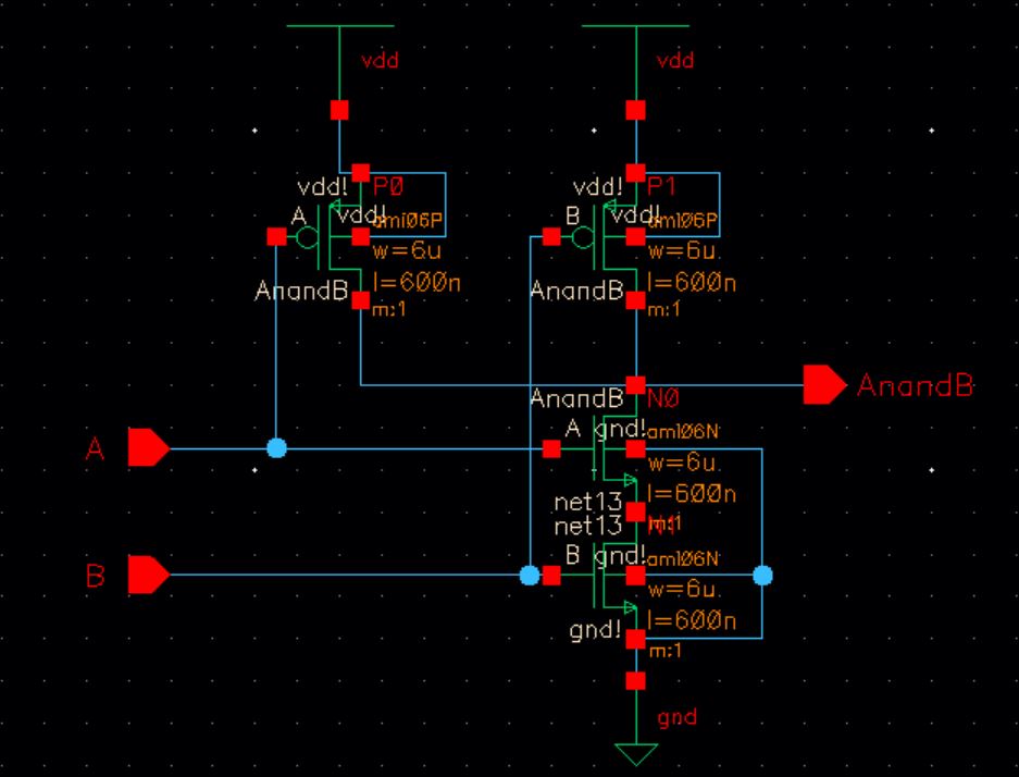
                Schematic and Simulation of 12u/6u inverter, NAND, and XOR  

Schematic of inverter, NAND, and XORSimulated using SpecterTruth Table
http://cmosedu.com/jbaker/courses/ee421L/f17/students/abera/lab6/Sim_NAND_XOR_INV_schem.JPGhttp://cmosedu.com/jbaker/courses/ee421L/f17/students/abera/lab6/Sim_NAND_XOR_INV.JPG
ABNAND
001
011
101
110
ABXOR
000
011
101
110

The inputs for each gate is a voltage pulse source that can represent the logic "0" as voltage value of "0 V" or ground and the logic "1" is represented as "5 V".  The simulation shows the gates i constructed mach the truth table outputs for the given inputs.   Once the gates are tested for valid logic the layout process begins.  


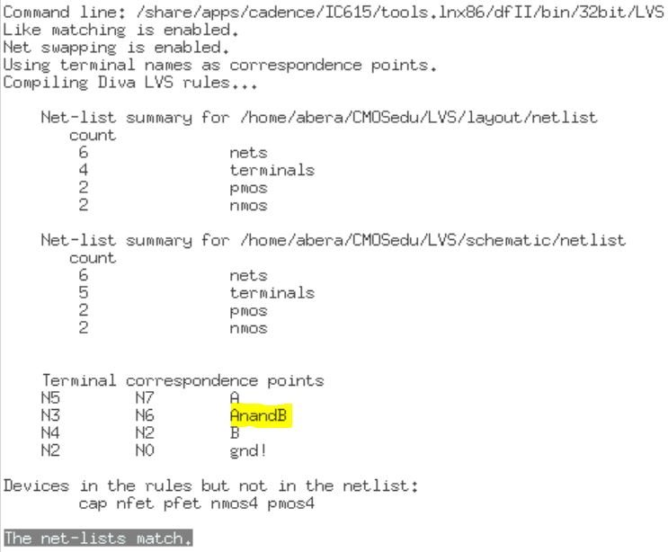
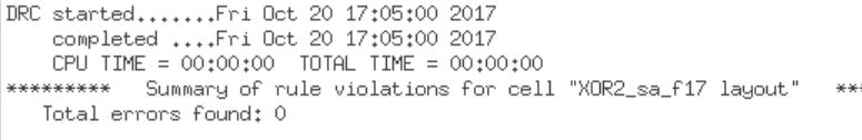
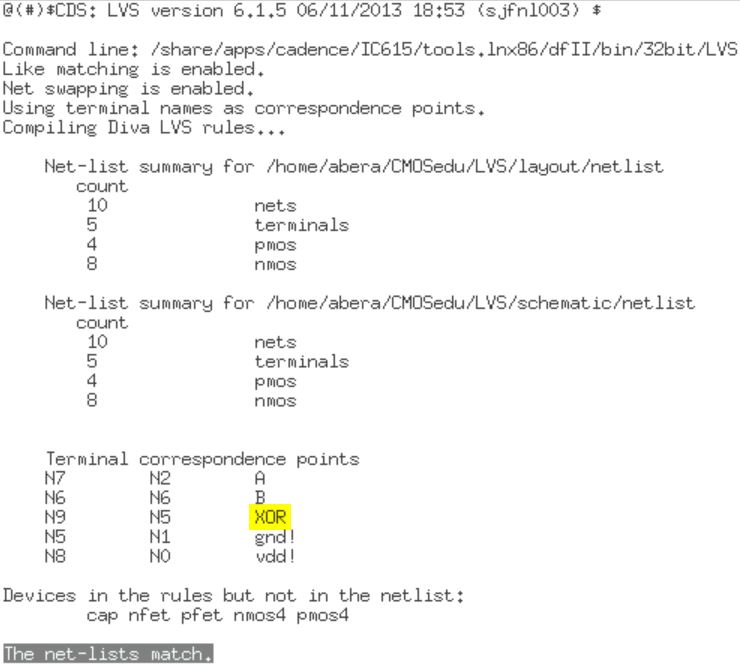
                                                           Layout of the NAND, and XOR  

NAND LayoutXOR Layout
http://cmosedu.com/jbaker/courses/ee421L/f17/students/abera/lab6/NAND/nand_Layout.JPG
http://cmosedu.com/jbaker/courses/ee421L/f17/students/abera/lab6/XOR/xor_Layout.JPG

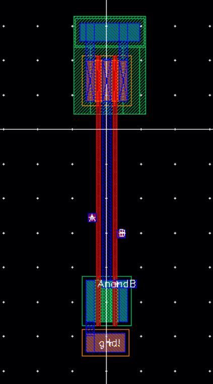
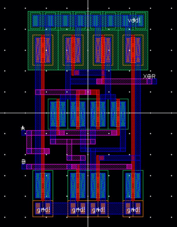
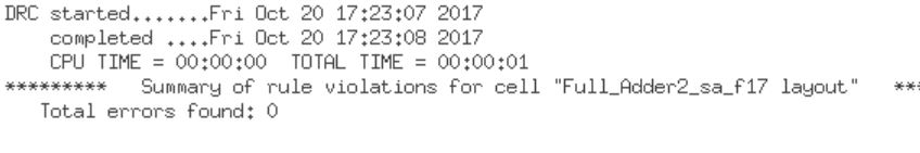
During the layout process the gates were constructed so that the the gates can be placed in parallel and having the same height.  This method allows for the power and ground to be roughted above and below.   Each gate has passed the DRC and the LVS net-list maches.


 NAND DRC and LVSXOR DRC and LVS
http://cmosedu.com/jbaker/courses/ee421L/f17/students/abera/lab6/NAND/nand_DRC.JPG


http://cmosedu.com/jbaker/courses/ee421L/f17/students/abera/lab6/NAND/nand_LVS.JPG
http://cmosedu.com/jbaker/courses/ee421L/f17/students/abera/lab6/XOR/xor_DRC.JPG
http://cmosedu.com/jbaker/courses/ee421L/f17/students/abera/lab6/XOR/xor_LVS.JPG


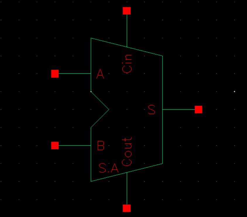
                                Schematic and Layout of the Full Adder
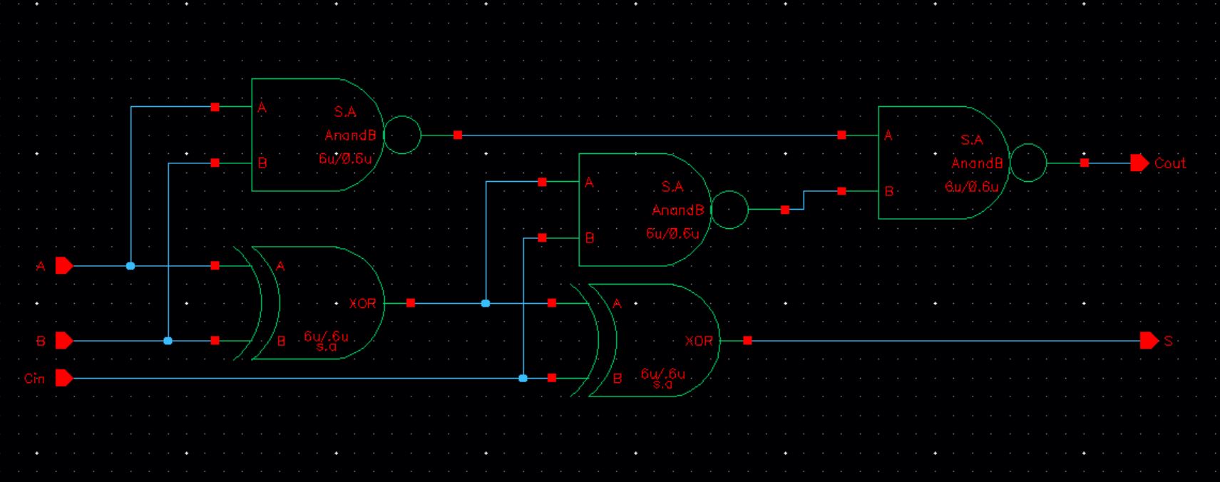
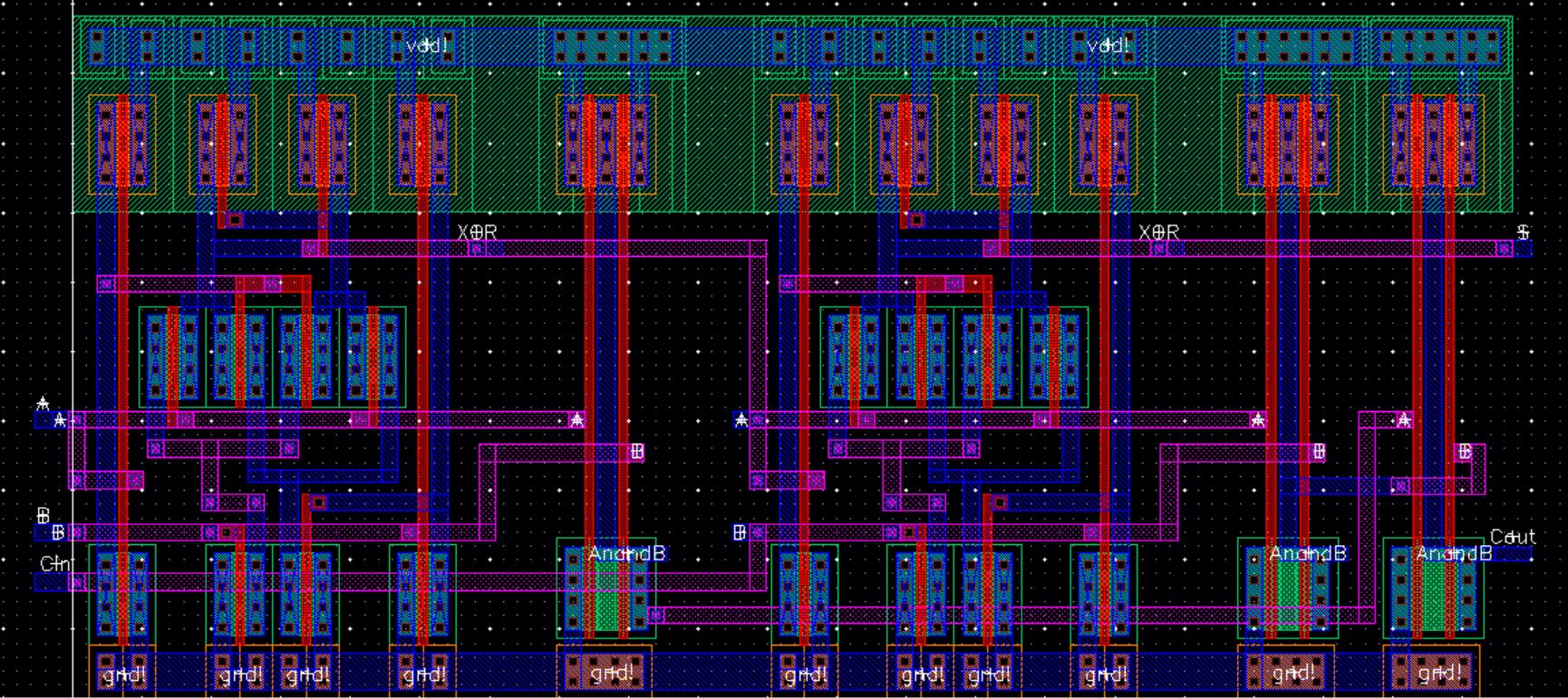
http://cmosedu.com/jbaker/courses/ee421L/f17/students/abera/lab6/Full%20Adder/Full%20Adder_Schematic.JPG
http://cmosedu.com/jbaker/courses/ee421L/f17/students/abera/lab6/Full%20Adder/Full%20Adder_Layout.JPG
The Full Adder schematic is relized by using the NAND and XOR gates created above.  The Full Adder circuit is then laid out using the layout of each gate and they were placed next to eachother in parallel and power is roughted at the top of the layout and ground on the bottom of the layout.

Full Adder SymbolFull Adder Layout DRC and LVS
http://cmosedu.com/jbaker/courses/ee421L/f17/students/abera/lab6/Full%20Adder/Full%20Adder_Symbol.JPGhttp://cmosedu.com/jbaker/courses/ee421L/f17/students/abera/lab6/Full%20Adder/Full%20Adder_DRC.JPG
http://cmosedu.com/jbaker/courses/ee421L/f17/students/abera/lab6/Full%20Adder/Full%20Adder_LVS.JPG
The Full Adder circuit is contained in the Full Adder symbol which can be used for simulating the Full Adder or it can be used as part of a more complicated circuit.
 
 
Simulation of Full AdderSimulated using SpecterTruth Table
http://cmosedu.com/jbaker/courses/ee421L/f17/students/abera/lab6/sim_full_adder.JPGhttp://cmosedu.com/jbaker/courses/ee421L/f17/students/abera/lab6/sim_full_adder%20plot.JPG
ABCinSCout
00000
00110
01010
01101
10010
10101
11001
11111

The full adder circuit is simulated by using three pulsed voltage source.  Inputs "A", "B", "Cin" are attaced to V0, V1, and V2 respectively will produce outputs "S" and "Cout".  
   

Lab6 files


Return to Abera lab

Return to EE 421L Labs