Analog Integrated Circuit Design Laboratory
Laboratory Report 9: Design of a Beta-Multiplier Reference (BMR) using the CD4007 CMOS transistor array
EMAIL: mesah1@unlv.nevada.edu
04-22-2020
Due to laboratory restrictions set by Clark County School District to avoid the spread of Covid-19, experimental results in this laboratory are borrowed from student reports from previous semesters. Link to citations used in this laboratory are located at the end of this report.
In this lab you may need to use two,
or more, CD4007 chips from the same production lot (see date code on
the top of chip) to ensure using a BMR to bias a current mirror is
possible. If the CD4007 chips are not from the same production lot they
will not "match" so current mirrors will not be possible.
- Build your BMR design and characterize it as you did in the pre-lab (if you use two chips ensure that grounds and VDDs of both chips are tied together).
- You
expect the BMR to become unstable if there is a large capacitance
across the resistor, such as a scope probe (important), so care must be
exercised
- Use your BMR to bias, and thus create, a:
- NMOS current mirror
- PMOS current mirror
- Measure how the current varies through each current mirror as the voltage across the mirror changes.
- Of course the current in the NMOS (PMOS) current mirror goes to zero as the voltage on the drain of the output device moves towards ground (VDD)
- Using these current mirrors drive two gate-drain connected transistors
- For the first experiment use the NMOS current mirror to drive two PMOS gate-drain connected devices.
- Use the voltages on the gate-drain connection of the two devices to bias a cascode current mirror (characterize this mirror as before)
- For the second experiment switch, that is, use the PMOS current mirror to drive two NMOS gate-drain connected devices.
- Again, use these two voltages to bias an NMOS cascode current mirror then characterize.


Simulation:


Experimental Results:

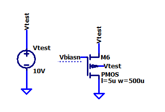
Schematics:


Simulation

Cascode Simulation


Experimental Results:


Simulation


Cascode Simulation


Experimental Results:


- http://cmosedu.com/jbaker/courses/ee420L/s17/students/ferret1/Lab%209/lab9.html
- http://cmosedu.com/jbaker/courses/ee420L/s19/students/kerstett/lab_9/lab_9.htm
- http://cmosedu.com/jbaker/courses/ee420L/s19/students/matacarl/Lab%209/LAB9.htm
- http://cmosedu.com/jbaker/courses/ee420L/s17/students/garrod/Lab%209/Lab%209.htm
- http://cmosedu.com/jbaker/courses/ee420L/s17/students/sanchezf/lab9/lab9.htm