Lab 9 Design of Beta-Multiplier Reference (BMR)- EE 420L
Authored
by Jeremy Garrod
4/19/2017
garrod@unlv.nevada.edu
Pre-Lab work
Pre-lab work
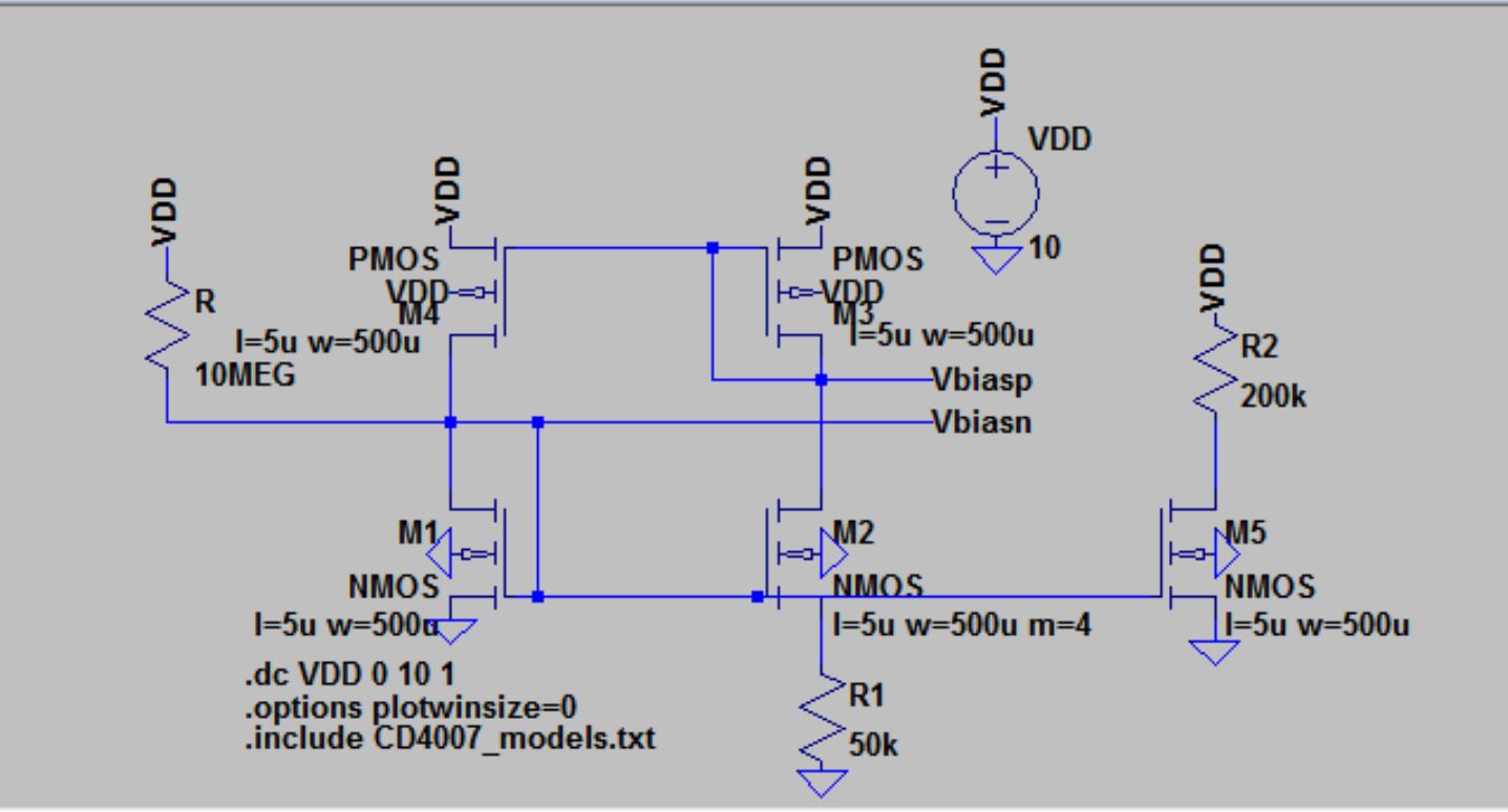
- This lab will use the level=1 MOSFET model created in lab 8 and, again, the MOSFETs in the CD4007.pdf CMOS transistor array.
- Design and simulate the operation of a BMR that biases the NMOS devices so that they have a gm of 20 uA/V
- Use a simple (big) resistor to VDD for the start-up circuit (explain how the addition of a resistor ensures start-up).
- When
the BMR is operating the current in the big resistor should be much
smaller than the current flowing in each branch of the BMR
- Write-up,
similar to a homework assignment, your design calculations and
simulation results. (This will count as the pre-lab quiz.)
- Ensure that you show the following in what you turn in:
- Hand calculations
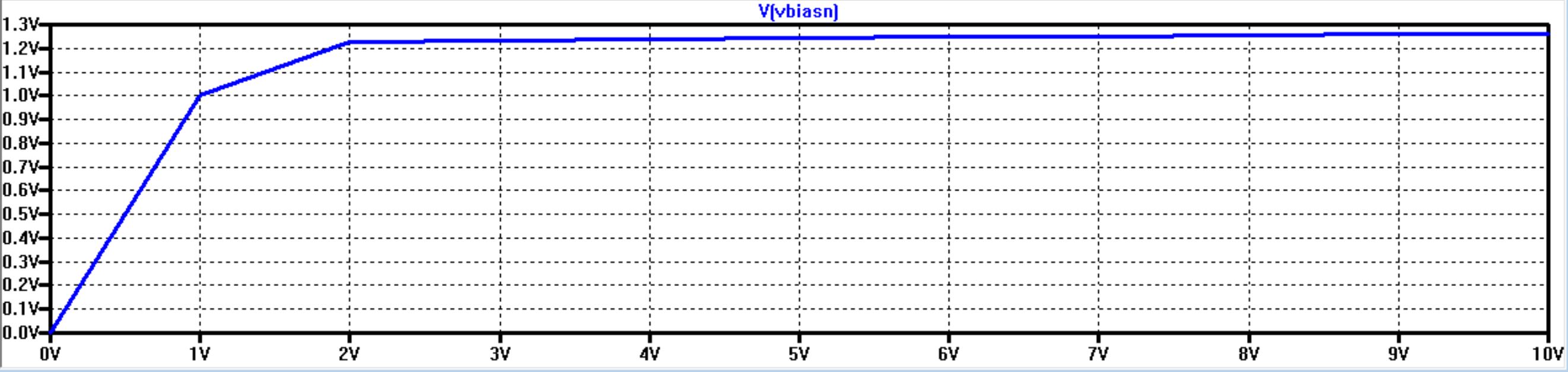
- Operation as VDD is swept from 0 to 10 V
- Vbiasn
should stabilize (be constant) after VDD hits a minimum value (estimate
this value of VDD assuming VGS/VSG is a threshold voltage and
VDS,sat/VSD,sat is zero).
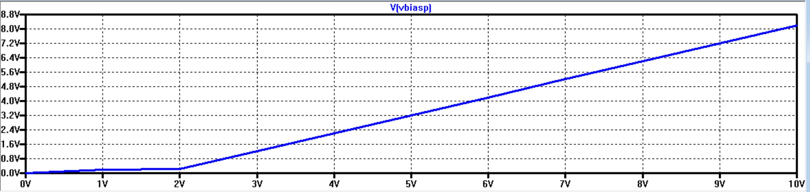
- Vbiasp should follow VDD after VDD hits a minimum value (show this in simulations)
- Unstable operation if too much capacitance is shunting the BMR's resistor (see bottom of page 630)
- Comments comparing the hand calculations with the simulation results
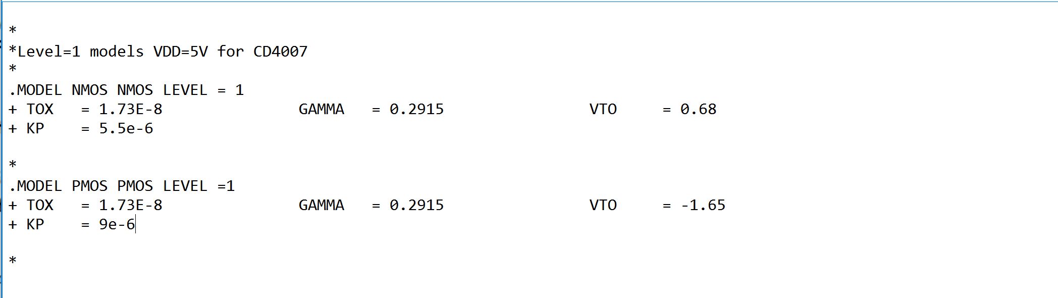
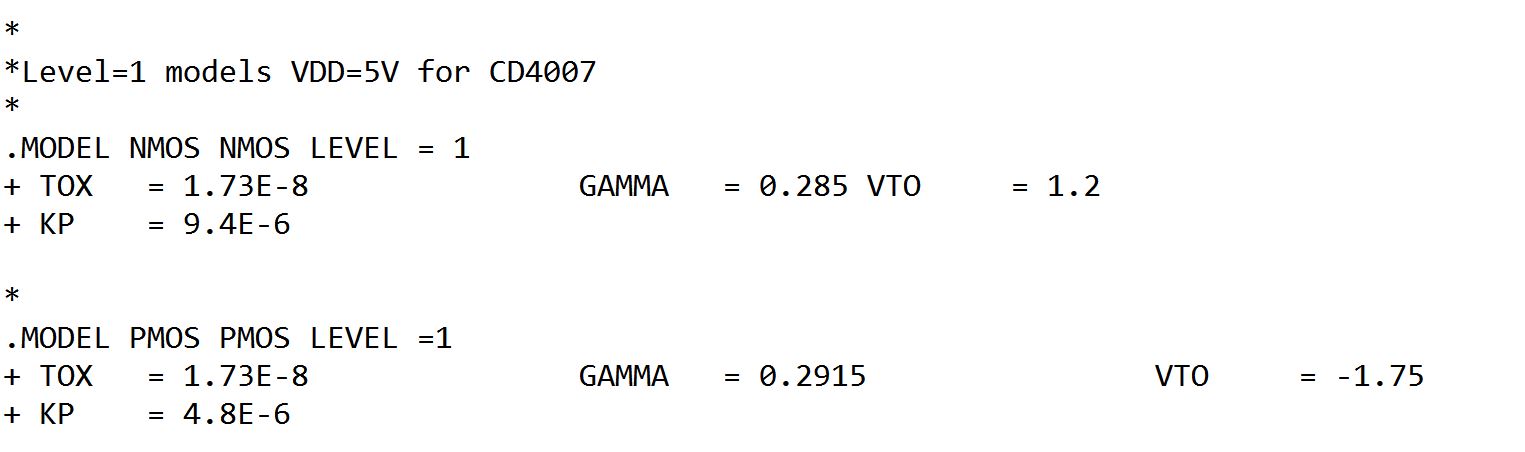
The
adjusted transistor parameters from laboratory 8 will be used in the
BMR design in this lab. Below is a summary of the transistor parameters
and the hand calculations.
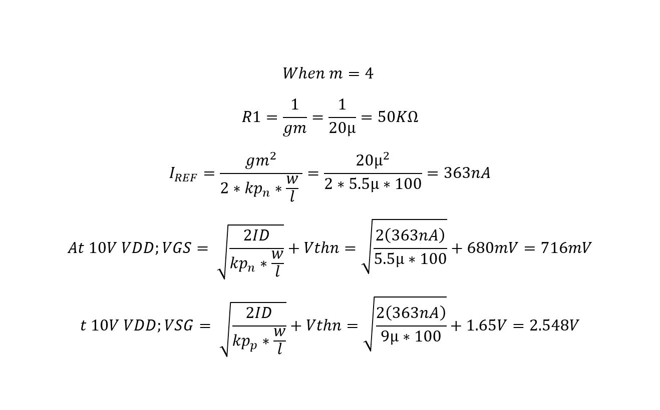
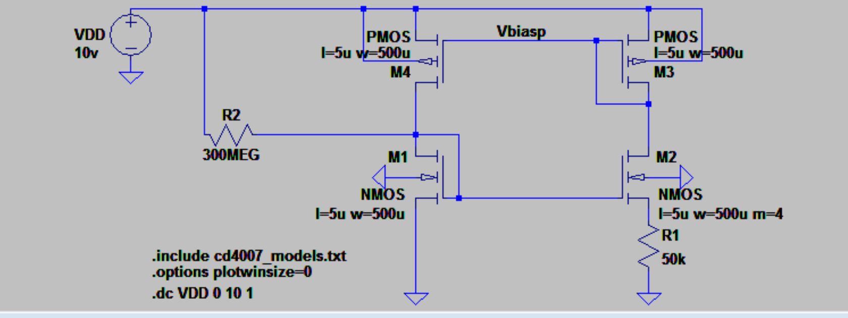
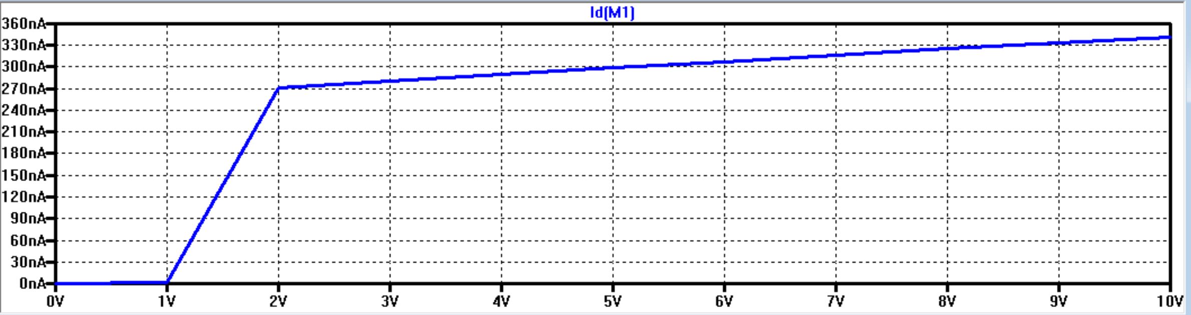
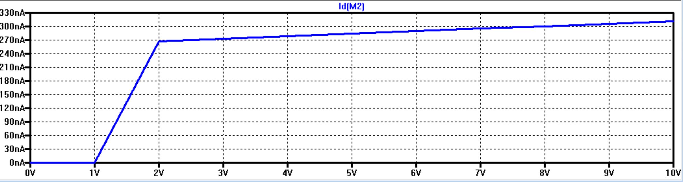
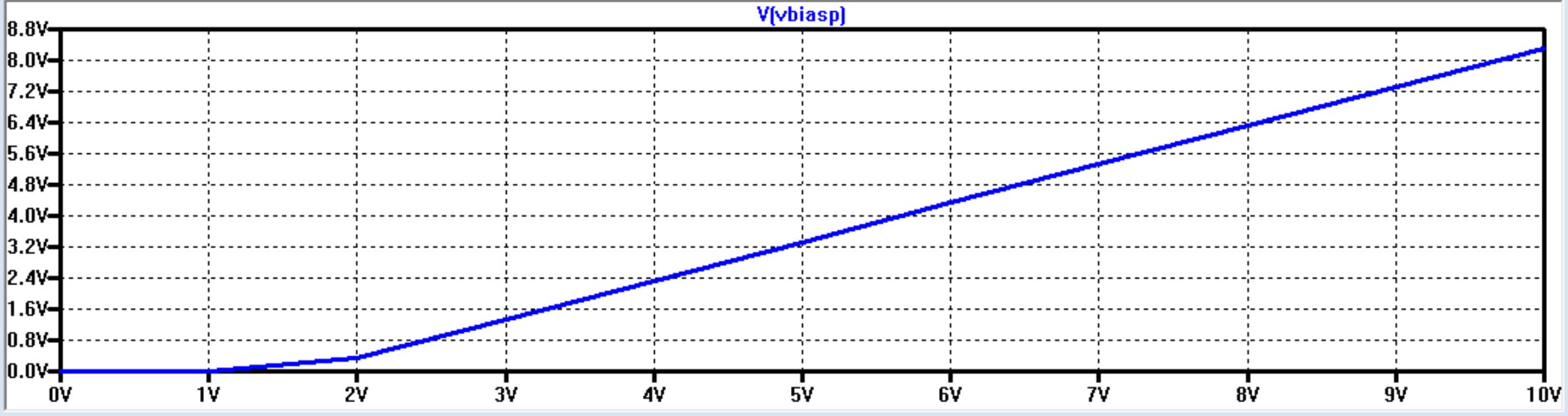
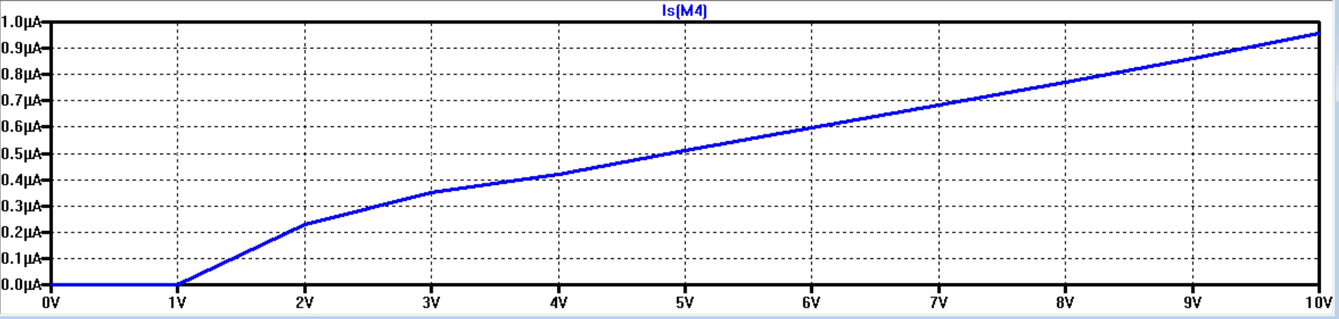
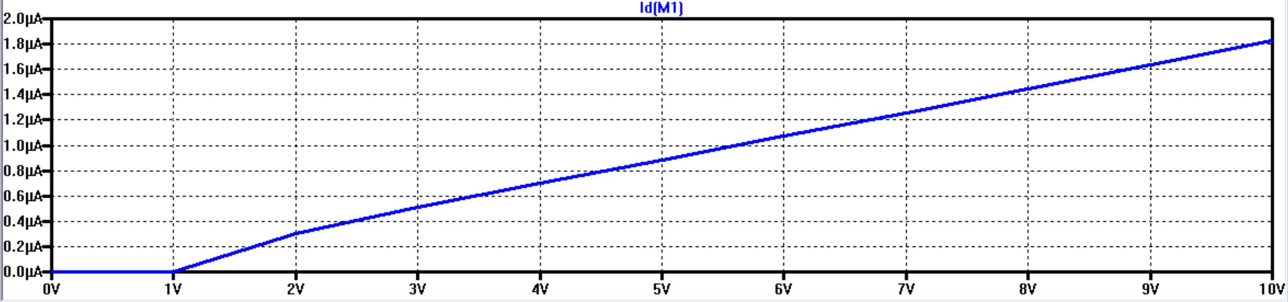
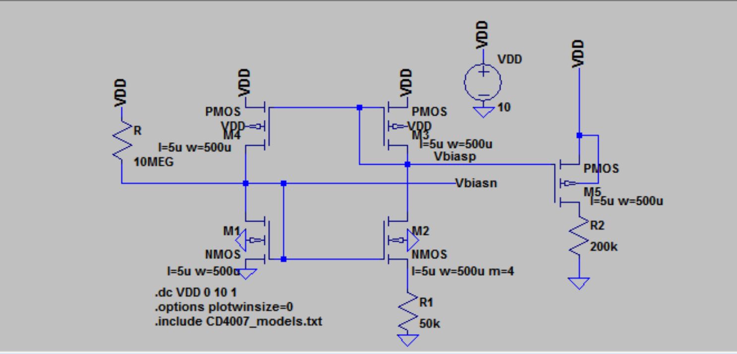
Below
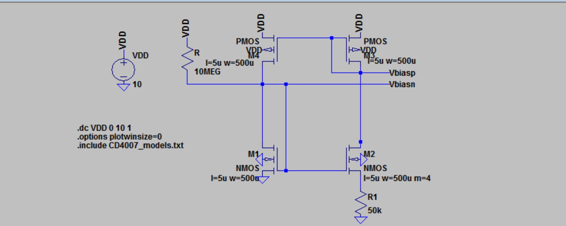
is the schematic of the BMR as well as the simulation results showing
the current through both sides, vbiasp and vbiasn while VDD varies from
0-10V in 1V steps. The simulations match closely to my hand
calculations. Vbiasn stays constant around 700mV and Vbiasp is always
about 2.5V below VDD. The current through both sides is almost
identical as well.

Lab Work
- Build your BMR design and characterize it as you did in the pre-lab
- You
expect the BMR to become unstable if there is a large capacitance
across the resistor, such as a scope probe (important), so care must be
exercised
Design
Sadly,
the wrong transistor array was used in laboratory 8 as well as the
prelab. In order to do this lab, the correct transistor array needed to
be characterized. The SPICE parameters can be seen below, I have
skipped writing all of the calculations, as that has already been done
that in the previous lab.
Another
issue that was encountered was when the vbiasn was being measured, it
would raised linearly until about 4.5V and then it jump and plateau. The
vbiasn would then stay at this voltage until VDD was lowered to around
2V, which is what was expected. The only remedy that seemed to work was
lowering the resistor value of the startup circuit. This in turn added
more current to the bottom NMOS devices than I would have liked. This
effect can be seen and will be further discussed below.
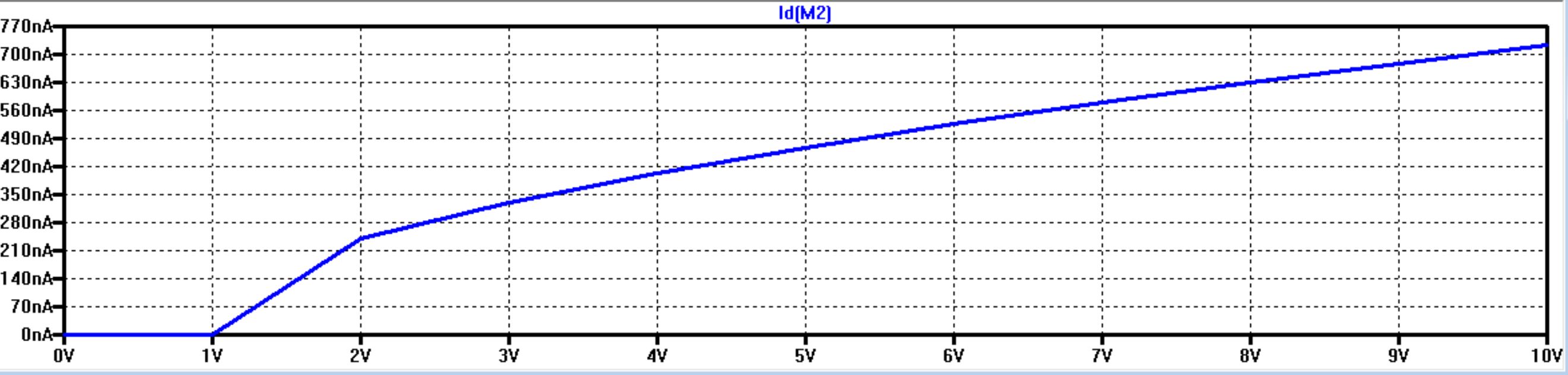
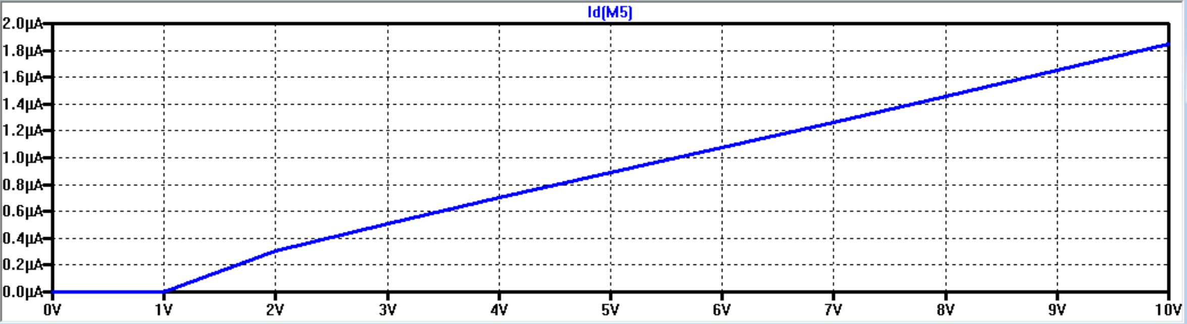
When
the VDD is at 10volts, it adds approximately 1uA of current into the
circuit, which causes the NMOS to have nearly double the current as the
PMOS, which can be seen in the simlation results above. Also, the
current in the right side of the BMR seems to be about 1/3 the
current in the left side. I had initially assumed that this was due to
the extra current from the start up circuit. With a 300MEG resistor, the gap is
not as large, but there is still a sizeable gap there. I am not
sure what could cause this, my only guess is that the SPICE parameters
are incorrect.
Experimental Results
In the table below, the current
through M2 is more precise than the current through M1. This is due to
the fact that M1 was measured directly with an ammeter that couldn't
measure lower than a tenth of a microamp. The current
through m2 was calculated by taking the voltage drop across the
resistor and dividing it by the resistance.
| VDD | Vbiasn | Vbiasp | ID M1 (uA) | ID M2 (uA) |
| 1 | 0.493 | 0.0176 | 0 | 0 |
| 2 | 1.015 | .536 | 0.9 | 1.22 |
| 3 | 1.151 | 1.545 | 1.4 | 1.36 |
| 4 | 1.544 | 2.569 | 1.7 | 1.44 |
| 5 | 1.556 | 3.463 | 1.9 | 1.54 |
| 6 | 1.561 | 4.437 | 2.1 | 1.60 |
| 7 | 1.569 | 5.398 | 2.3 | 1.68 |
| 8 | 1.574 | 6.421 | 2.9 | 1.75 |
| 9 | 1.597 | 7.533 | 3.2 | 1.83 |
| 10 | 1.609 | 8.429 | 3.3 | 1.89 |
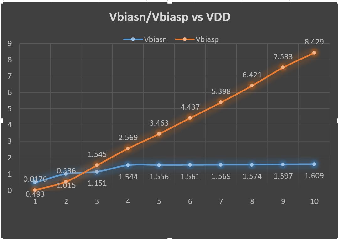
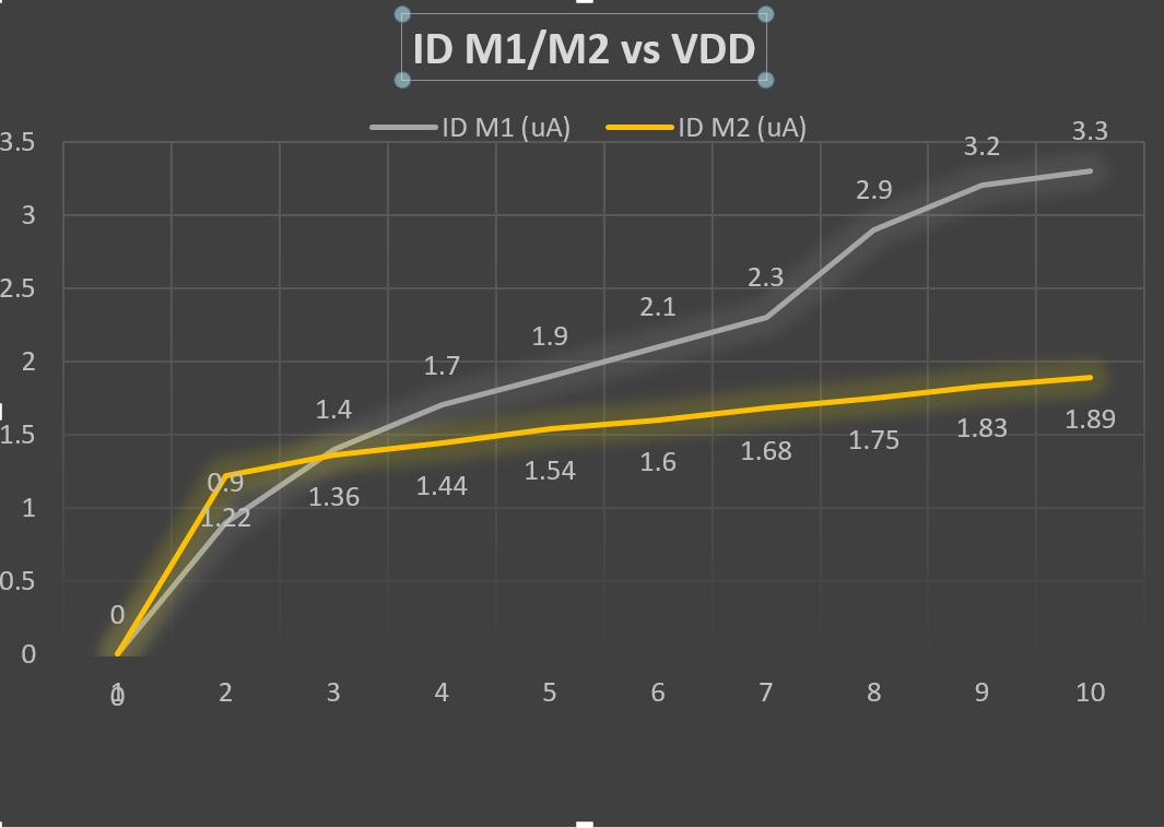
It
can be seen that the right side of the BMR has the exact behavior that
you would expect to see. However, the left side is very distorted,
which is more than likely due to the extra current from the start up
circuit. Neither of the measured current are really close to the
simulated values. The left side is roughly 1.5x the simulated current
and the right side is about 2.5x the simulated current.
- Use your BMR to bias, and thus create, a:
- NMOS current mirror
- PMOS current mirror
- Measure how the current varies through each current mirror as the voltage across the mirror changes.
- Of
course the current in the NMOS (PMOS) current mirror goes to zero as
the voltage on the drain of the output device moves towards ground (VDD)
Design
The current through the NMOS current mirror is the same as the current in M1, which is expected. 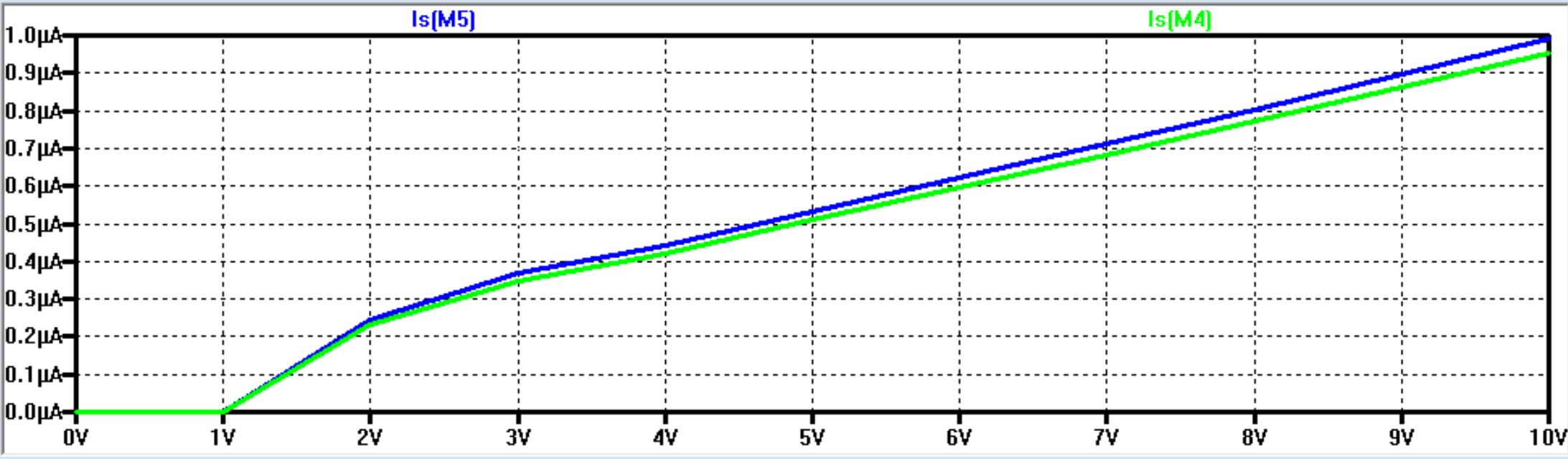
The
current in M5 is close to the current that flows in M4. It is close
enough to where I'd say that the current mirror is working as
intended.
Experimental Results
| VDD | ID NMOS Mirror (uA) | ID PMOS Mirror (uA) |
| 1 | 0 | 0 |
| 2 | 0.9 | 2.5 |
| 3 | 1.1 | 3 |
| 4 | 1.5 | 3.6 |
| 5 | 1.8 | 4.1 |
| 6 | 2 | 4.2 |
| 7 | 2.3 | 4.9 |
| 8 | 2.7 | 5.3 |
| 9 | 2.9 | 5.9 |
| 10 | 3.4 | 6.5 |
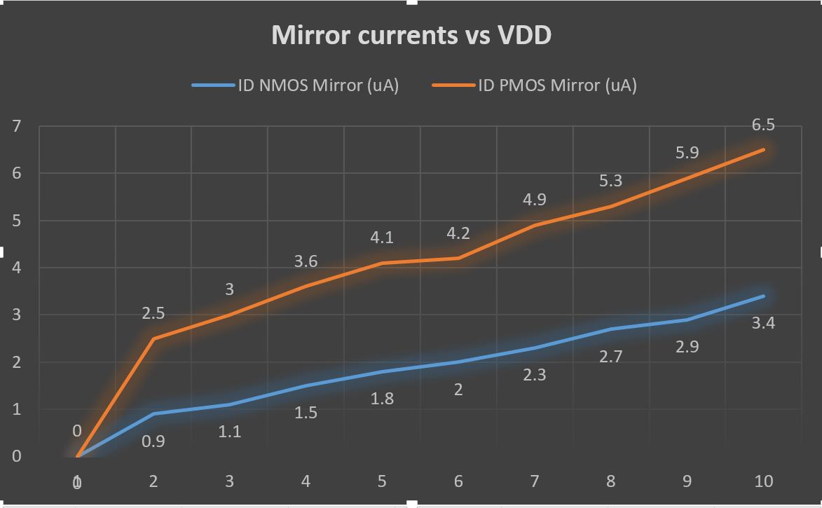
The
currents that were measured in the lab were pretty far off from the
simulations. The NMOS current mirror has roughly double the current
while the PMOS current mirror has over 5x the simulated current. even
though the values were off, the shapes of the graphs are very similar
to those from the simulations.
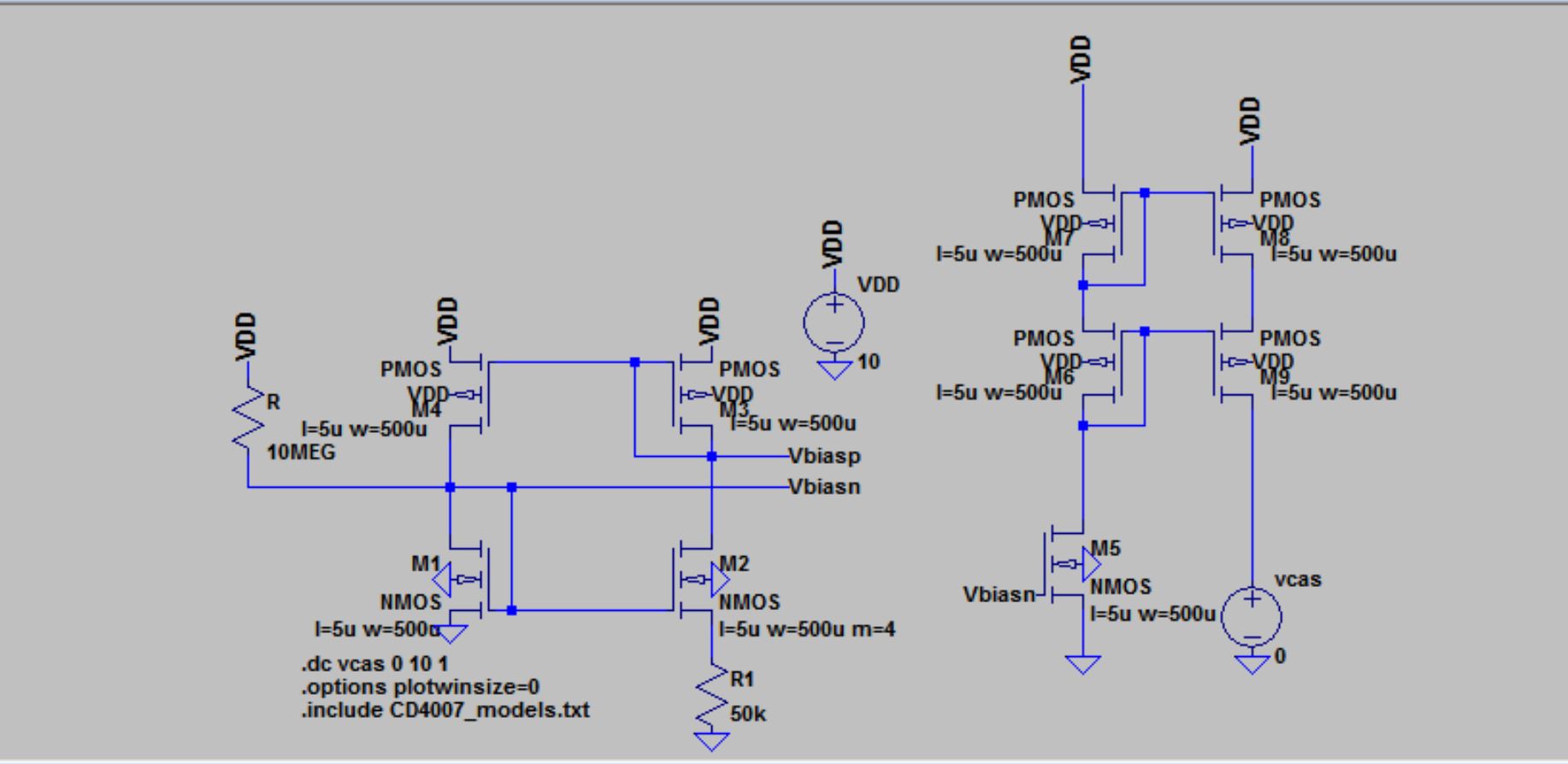
- Using these current mirrors drive two gate-drain connected transistors
- For the first experiment use the NMOS current mirror to drive two PMOS gate-drain connected devices.
- Use
the voltages on the gate-drain connection of the two devices to bias a
cascode current mirror (characterize this mirror as before)
- For the second experiment switch, that is, use the PMOS current mirror to drive two NMOS gate-drain connected devices.
- Again, use these two voltages to bias an NMOS cascode current mirror then characterize.
Design
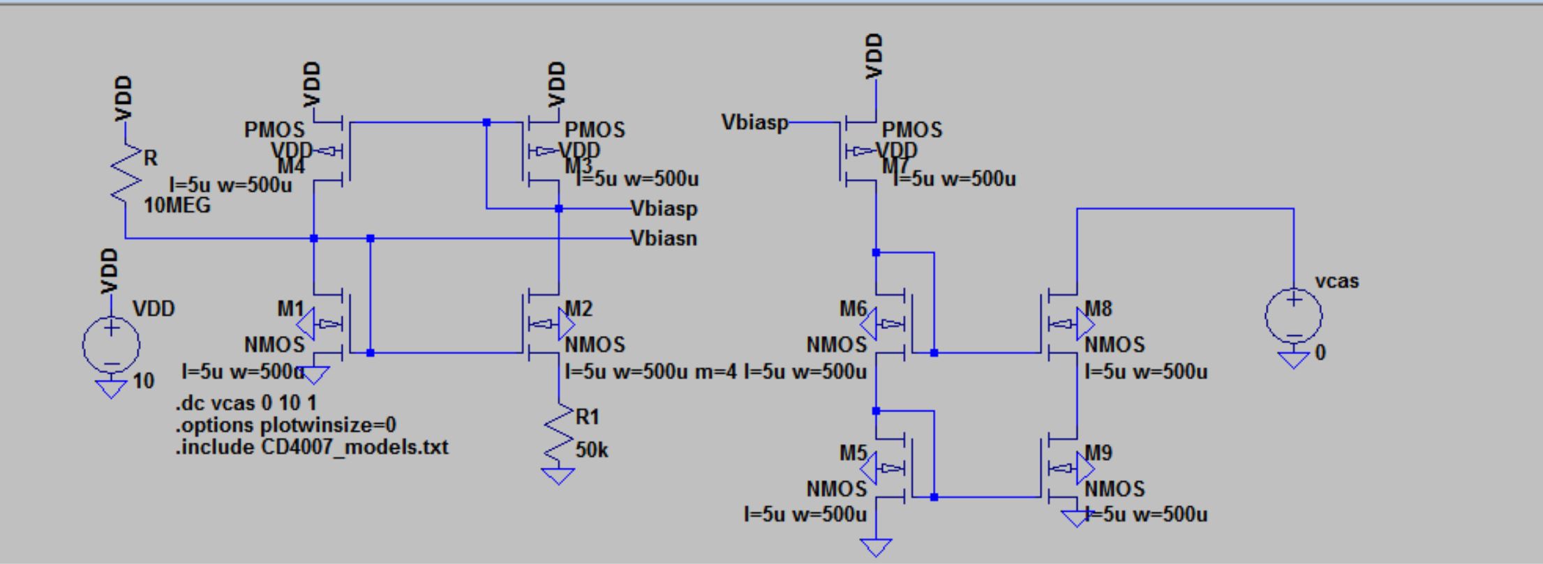
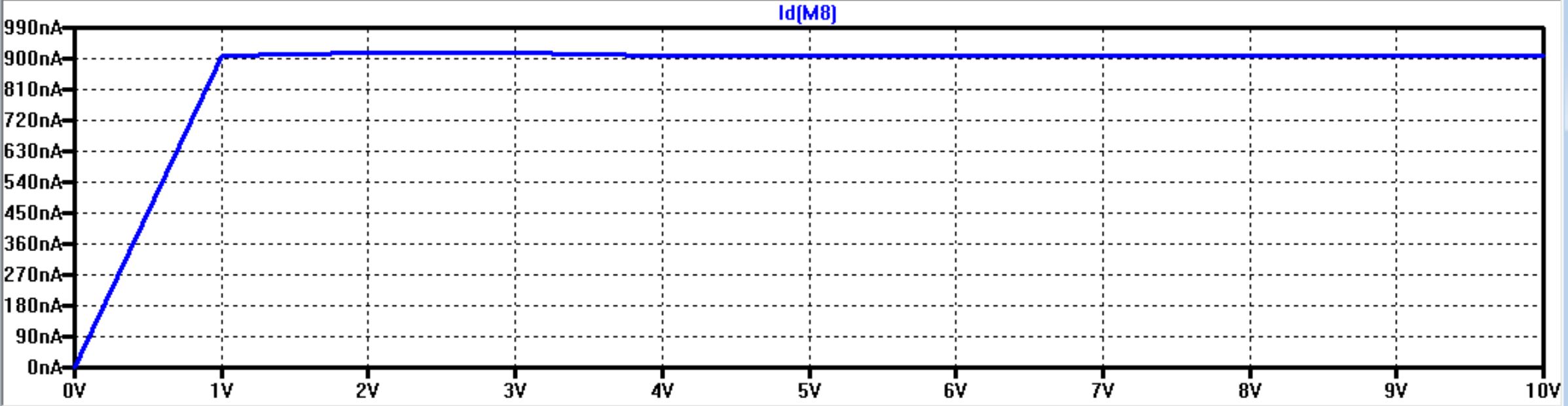
The
NMOS cascode is working as intended in the simulations, it is acting
like a constant current source with very little variation.
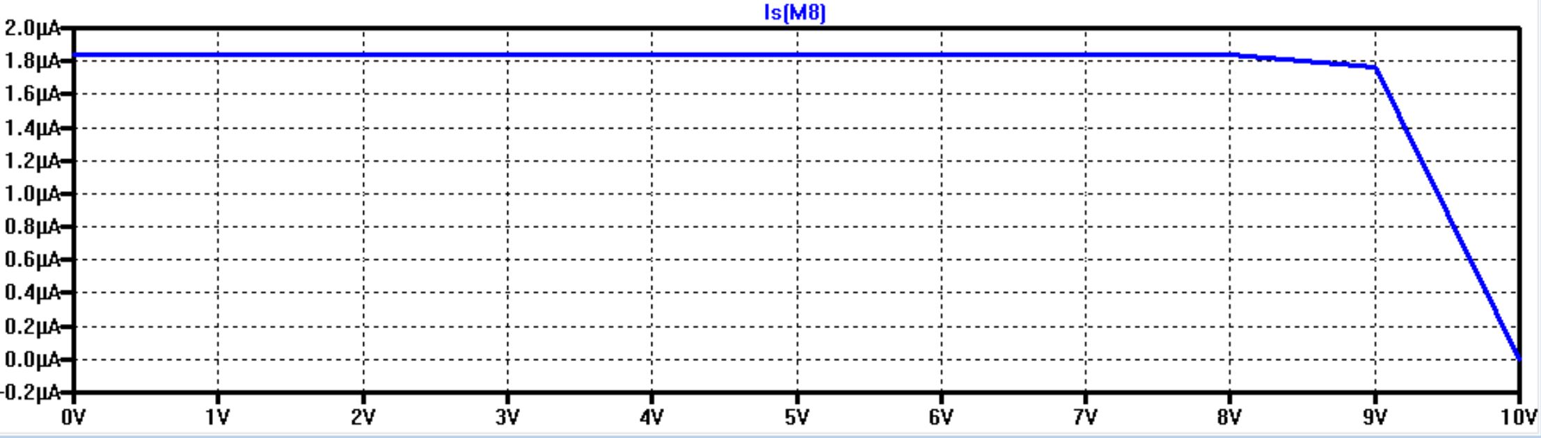
It looks like the PMOS cascode is working, but I am not too sure.
Experiment
I was not able to get my PMOS cascode to work in the lab. I do not know
if there was an issue with the actual circuit or my testing methodology.
| VDD | NMOS Cascode (uA) |
| 0 | 1 |
| 1 | 6 |
| 2 | 6 |
| 3 | 6 |
| 4 | 6.1 |
| 5 | 6.2 |
| 6 | 6.3 |
| 7 | 6.3 |
| 8 | 6.3 |
| 9 | 6.4 |
| 10 | 6.5 |
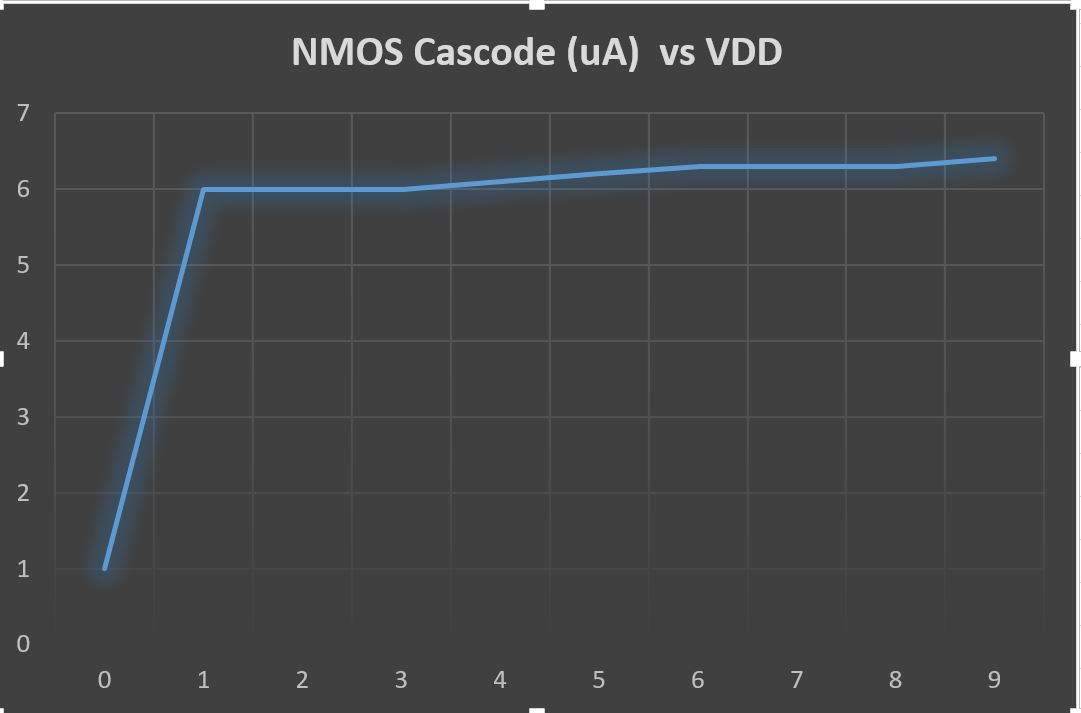
This
experiment ended up being similar to the otherexperiments, the shape is
very close to what was simulated, but the actual values are pretty far
off.
While
the shapes of my graphs seemed to follow those from the simulations, I
could not get my measured values to match my simulations. I am assuming
that my KP values that I am using are off from the real values. I am
also putting a relatively large amount of current into the current
mirror from the start up circuit, when it should be a negligible amount. I am positive that this
has an adverse affect on the circuit, however, the smaller resistor was
necessary in order to get the correct behavior.
Return to EE 420 Labs