EE 420L
Analog
Integrated Circuit Design Laboratory
Laboratory
Report 9: Design of a Beta-Multiplier Reference (BMR) using the CD4007 CMOS
Transistor Array
AUTHOR:
Bryan Kerstetter
EMAIL:
kerstett@unlv.nevada.edu
APRIL
23, 2019
General
Overview
This
laboratory regards the design and implementation of a Beta-Multiplier Reference
(BMR). A BMR is a voltage and current reference. The structure of a BMR can be
described by a NMOS and PMOS current mirror that are cascoded. A BMR includes a
resistor R that is tied low and a
MOSFET with a β multiplication of K
(β*K). The R and K values determine the behavior of the
BMR. A general topology of a BMR can be seen in Figure 1.

Figure 1
Prelab
Laboratory 8 regarded the characterization of the CD4007
Transistor Array. The characterization resulted in the following two LTspcie models. These models will be used to design a BMR
in LTspice before implementation.
*
* Level=1 models of CD4007 Transistor Array
*
.MODEL N_Lab8 NMOS LEVEL = 1
+ TOX = 17.25e-9 VT0 = 1.6 KP = 6u
+ LAMBDA = 0.010 GAMMA = .01
.MODEL P_Lab8 PMOS LEVEL = 1
+ TOX = 17.25e-9 VT0 = -1.5 KP = 5u
+
LAMBDA =
0.030 GAMMA
= .5
We must design a BMR using the CD4007 transistor array. This BMR
should have a ![]() .
This is our BMR design requirement. We must prescribe R and K values that result in this design
requirement. Therefore, we must determine the reference current that produces
the needed trans-conductance.
.
This is our BMR design requirement. We must prescribe R and K values that result in this design
requirement. Therefore, we must determine the reference current that produces
the needed trans-conductance.
![]() [1]
[1]
![]() [2]
[2]
Now we may find the reference current with the following
parameters:
![]() [3]
[3]
![]() [4]
[4]
![]() [5]
[5]
![]() [6]
[6]
The reference current of a BMR can be defined by,
![]() [7]
[7]
Where ![]() and
and ![]() can be developed from the square law equations
such that
can be developed from the square law equations
such that
![]() [8]
[8]
![]() [9]
[9]
 [10]
[10]
![]() [11]
[11]
![]() [12]
[12]
The bias current or the reference current can be determined from
the resistance value R. Therefore, we
may set ![]() by
determining a value for R. We
may find this value by solving for R.
by
determining a value for R. We
may find this value by solving for R.
![]() [13]
[13]
![]() [14]
[14]
![]() [15]
[15]
Where,
k
= 2 [16]
![]() [17]
[17]
![]() [18]
[18]
![]() [19]
[19]
![]() [20]
[20]
![]() [21]
[21]
Allowing us to design the following circuit as seen in Figure 2. The purpose of resistor R2 is the start-up circuit as it
provides little current to ensure the BMR is functional. Two NMOSs in parallel
provide a beta-multiplication of 2 (widths of MOSFETs add together). Figure 3
and 4 demonstrate the simulation results of our beta-multiplier design.

Figure 2

Figure 3

Figure 4
The resistance value R1 can then be adjusted to 32kΩ.
This resistance change allows for design were the correct ![]() is achieved. Figures 5 and 6 show the
simulation results with a R1 resistance value of 32kΩ.
is achieved. Figures 5 and 6 show the
simulation results with a R1 resistance value of 32kΩ.

Figure 5

Figure 6
Operation as VDD sweeps from 0 to 10V

Figure 7
Previously in EE 420: Homework 11, we saw that if the
decoupling capacitors are too small the circuit becomes unstable.
NOTE: This question uses the MOSFETs as given by
the Long Channel Process in Dr. Baker’s CMOS book.

Figure 8: Problem 20.10 in Dr. Baker’s CMOS book
Without reducing the size of MCP and MCN.

Figure 9
DC Sweep from 0-2 V of VDD.

Figure 10
Transient simulation for 500ns.

Figure 11
Capacitor size reduced to 100n/100n.

Figure 12
DC Sweep from 0-2 V of VDD.

Figure 13
Transient simulation for 500ns.

Figure 14
As seen above, the circuit becomes unstable.
Now, we may go back to
our BMR design and attempt to make our design unstable. Adding decoupling
capacitors to our recently designed circuit.

Figure 15

Figure 16
Now we may try to add a
large shunt capacitance to see if the circuit becomes unstable.

Figure 17

Figure 18
The
circuit does not become unstable. However, we saw earlier that the beta
multiplier can be unstable. It is assumed that our spice models are two
rudimentary to accommodate the desired unstableness.
Description
of Laboratory Procedures
The circuit as seen in Figure 19 depict the circuitry
implemented on the breadboard (Figure 20). The entire BMR and current mirrors was
implemented on two CD4007 transistor arrays. Unfortunately, there were no more
CD4007 chips. Therefore, we had to implement the cascoded current mirrors on
four CD4007UB chips. Using both CD4007 and CD4007UB chips will result in a
current mismatch. To characterize the current mirrors and cascoded current
mirrors we will vary the voltage across the mirrors and inspect the drain
currents in the mirror.

Figure 19

Figure 20
Experimental
Reference Voltages
Table 1
|
|
LTspice |
Experimental
|
|
VrefN (V) |
1.647 |
1.480 |
|
VrefP (V) |
3.455 |
3.528 |
In Table 1, we see that our reference voltages
observed in LTspice and our experimental results are
in agreement.
Current
Mirror Characterizations
In Figures 21-24, one can see the current mirror
characterizations that were executed. On the right-hand side of each image, one
may see our experimental results. Whereas, on the left-hand side, one may see
the LTspice simulation output. There are differences
between our LTspice and experimental results. This
discrepancy is due to a current mismatch. This current mismatch is most likely
attributed to using both CD4007 and CD4007UB chips (as mentioned previously).
CLICK HERE FOR THE CAPTURED
DATA
NMOS
Current Mirror

Figure 21
PMOS
Current Mirror
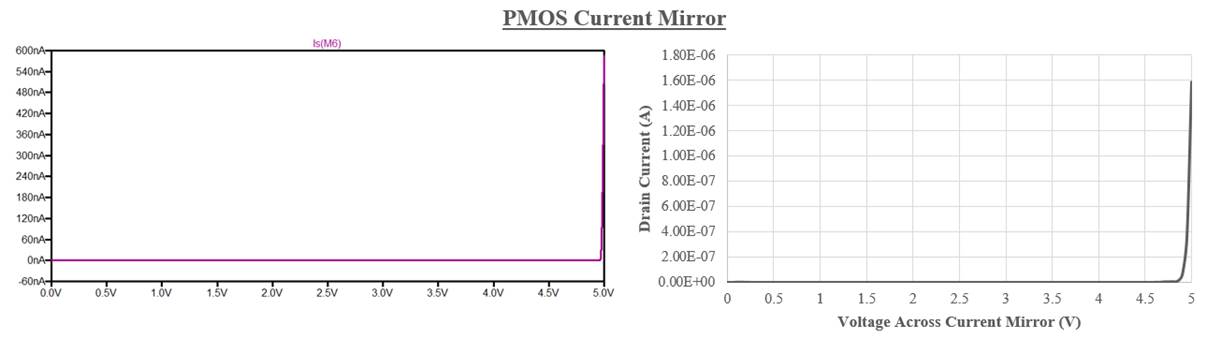
Figure 22
NMOS
Cascoded Current Mirror

Figure 23
PMOS
Cascoded Current Mirror

Figure 24
Return to EE
420L Spring 2019 Page
Return to Dr. Baker’s CMOSedu homepage
