Lab 9 - ECE 420L Engineering Electronics II Lab
Authored
by Frank Sanchez,
sanchezf@unlv.nevada.edu
4/19/2017
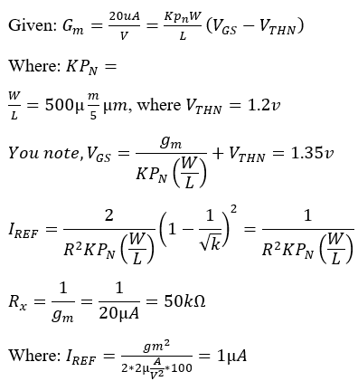
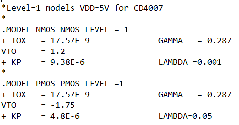
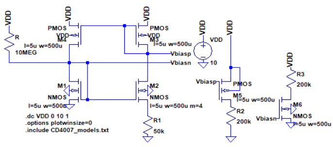
The hand calculations for the BMR design are displayed below, along with the parameters used for LTspice.
++++++++++++++
Experiment 1
++++++++++++++
- Build your BMR design and characterize it as you did in the pre-lab
- You
expect the BMR to become unstable if there is a large capacitance
across the resistor, such as a scope probe (important), so care must be
exercised
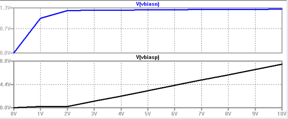
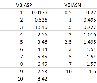
The experiment was challenging, due to it needing so many transistors. The wiring was a process.
The
simulation results were a close approximate to the experimental. The
experimental results showed a higher than expected result.
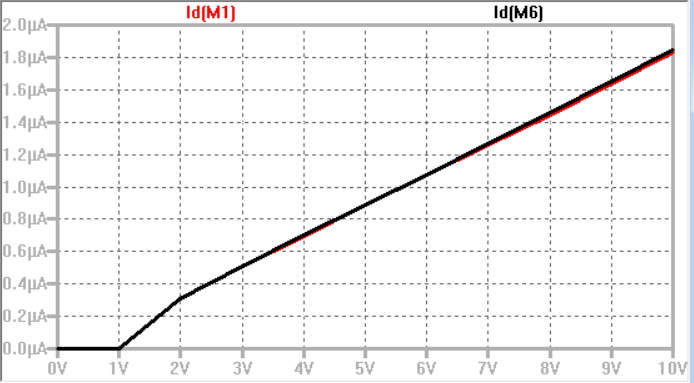
| LTspice | Expeimental |
 |  |
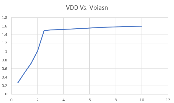
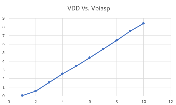
| Experimental Plot- Bias N | Experimental Plot- Bias P |
| 
|
| Id Vs. VDD | 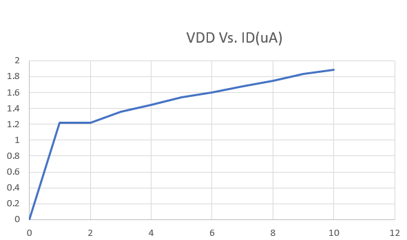 |
++++++++++++++
Experiment 2
++++++++++++++
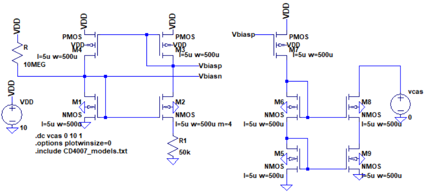
- Use your BMR to bias, and thus create, a:
- NMOS current mirror
- PMOS current mirror
- Measure how the current varies through each current mirror as the voltage across the mirror changes.
- Of
course the current in the NMOS (PMOS) current mirror goes to zero as
the voltage on the drain of the output device moves towards ground (VDD)
For
this experiment, i deceded to go with the 200k resistor in order to
sample my current going through the transister. This in hand made it
easier for me to find my desired values. | Schematic |
 |
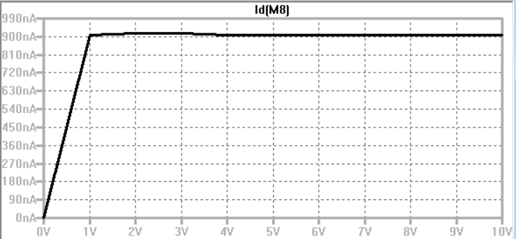
The simulations below show the drain current for both the NMOS and PMOS varied by the voltage supplied.
| NMOS Current Mirror | PMOS Current Mirror |
 | 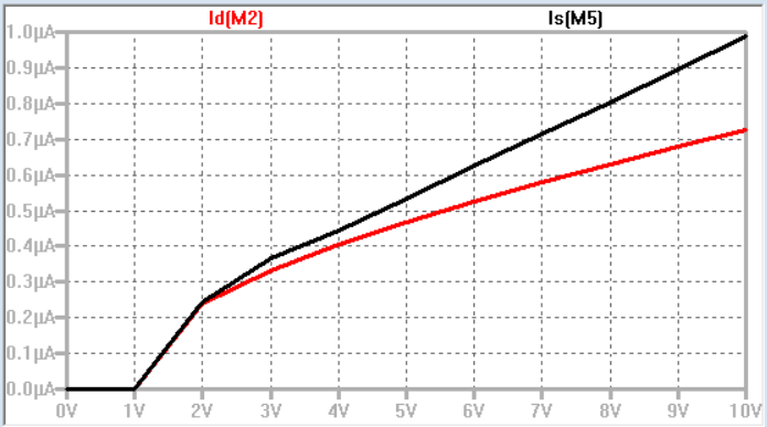 |
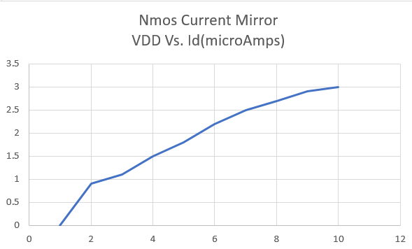
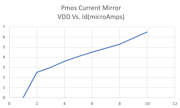
Experimental Results
The
experimental values are seen below for both Nmos and Pmos current
mirrors. All values recorded varying the power supply and recording the
current using the multimeter.
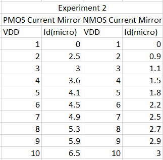
As
you can see, I came up with a higher current than my theoretical
results. This could have been due to bad wiring but after multiple
re-wirings this is what I came up with. It is definitely correlated to
the theoretical results, but just with a "higher" current uptake.
| NMOS | PMOS |
| 
|
++++++++++++++
Experiment 3
++++++++++++++
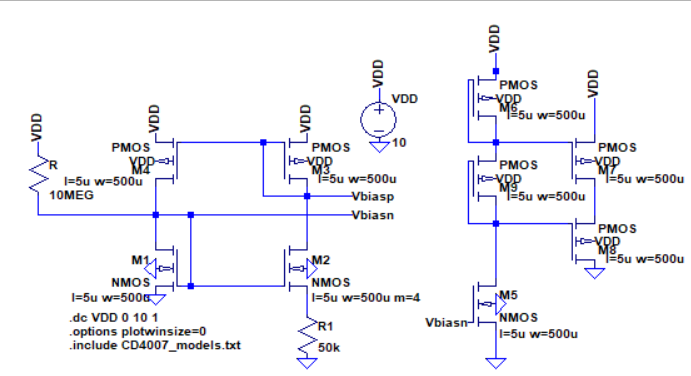
- Using these current mirrors drive two gate-drain connected transistors
- For the first experiment use the NMOS current mirror to drive two PMOS gate-drain connected devices.
- Use
the voltages on the gate-drain connection of the two devices to bias a
cascode current mirror (characterize this mirror as before)
- For the second experiment switch, that is, use the PMOS current mirror to drive two NMOS gate-drain connected devices.
- Again, use these two voltages to bias an NMOS cascode current mirror then characterize.
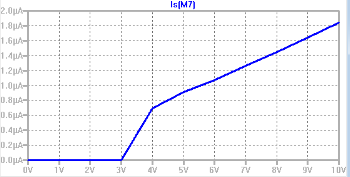
NMOS Cascode Current Mirror
| LTspice |
 |
Experimental Results
This table was made by varying the power supply and recording the values through the multimeter.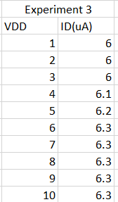
Values were plotted for visualization below.
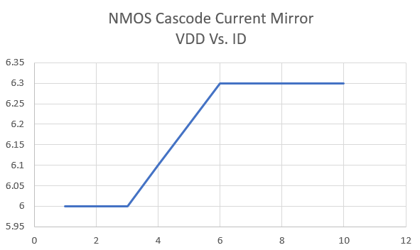
As
you can see the experimental values did not match the theoretical
values for this experiment. It might have had to do with the wiring for
the design or another fault.
PMOS Cascode Current Mirror
| LTspice |
|
Experimental Results
This table was made by varying the power supply and recording the values through the multimeter.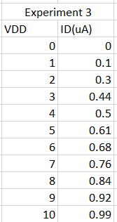
Values were plotted for visualization below.
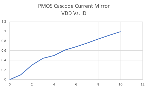
As
you can see the experimental values did not match the theoretical
values for this experiment. It might have had to do with the wiring for
the design or another fault.
++++++++++++++++++++++++++++++++++++++++++++++++++++++++++++++++++++++++++++++++
Lab Conclusion:
Experiment
9 gave me a good idea on how a BMR using the CD4007 transistor chip
works. This lab was verys similar to our last lab, due to it giving the
student an understanding on how to characterize a transistor. This lab
gave us an idea how a Beta-Multiplier Reference is layed out and tested
for characterization.
Return to EE 420L Labs