Jesus Flores-Arellano
Kanoa Hokoana
This lab will focus on the layout and submission preperation to MOSIS for device fabrication.
Tutorial 6 was completed prior to the start of this lab and all content was reviewed in its entirety.
Using
a 40 pin pad design, the devices listed below should be added being
sure to not allow any two devices to share a vdd connection to prevent
shorts to ground that would cause all devices to become inoperable.
Global ground can be shared amound devices located on pin 20.
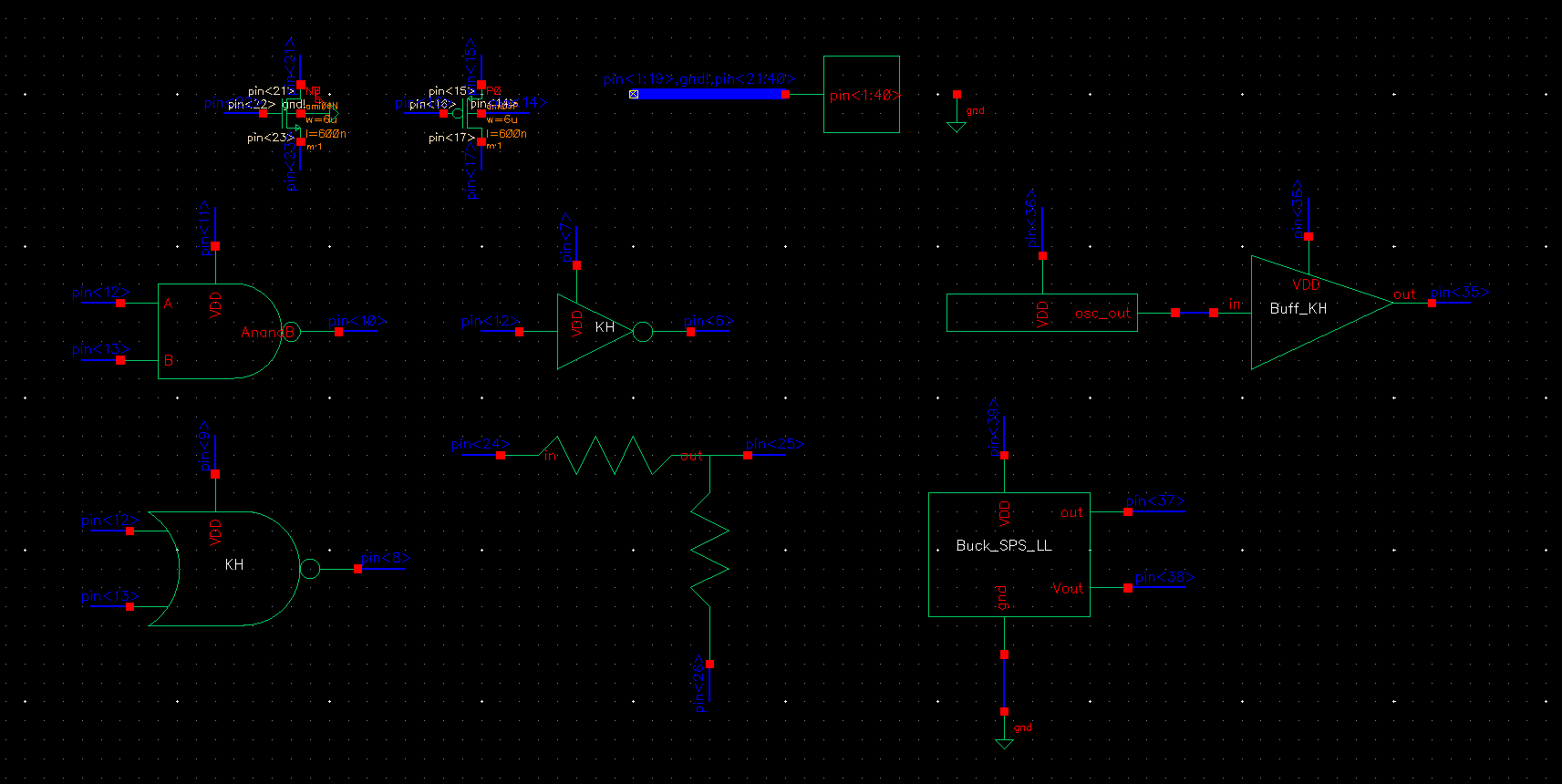
Devices Added to the Chip:
- Buck Switching Power supply from F_23 semester
- 31-stage ring oscillator with buffer circuit to drive a 20pF off-chip load
- 6u/600n NAND and NOR
- 12/6 inverter with minimum length
- 6u/600n PMOS and NMOS with all terminals connected to indivdual pins outside of global grounded NMOS
- 25K N-well resistor and 10K hi-res resistor forming a voltage divider
Pin
definitions, associated schematic and device locations should be
included along with a concise testing procedure to verfiy proper
operation of each device
Laboratory Procedure
Device list with pin locations shown below:
** NOTE: For many logical operations input Pins 12 & 13 are share among devices **
| Device | Pin# | Signal | Value |
| Common GND | 20 | input | gnd! |
| NOR Gate | 8 | Output | A NOR B |
| 9 | Input | vdd | |
| 12 | Input | A | |
| 13 | Input | B | |
| NAND Gate | 10 | Output | A NAND B |
| 11 | Input | vdd | |
| 12 | Input | A | |
| 13 | Input | B | |
| XOR Gate | 19 | Output | A XOR B |
| 18 | Input | vdd | |
| 12 | Input | A | |
| 13 | Input | B | |
| 12/6 Inverter | 6 | Output | Ai |
| 7 | Input | vdd | |
| 12 | Input | A | |
| NMOS(Bodu grounded to substrate) | 21 | Output | Drain |
| 22 | Input | Gate | |
| 23 | Input | Source | |
| PMOS | 14 | Input | Body |
| 15 | Input | Source | |
| 16 | Input | Gate | |
| 17 | Output | Drain | |
| 31 Stage + Buffer | 34 | Input | Enable |
| 35 | Output | Oscillator Ouput | |
| 36 | Input | vdd | |
| Voltage Divider | 24 | Input/Output | 25k Input |
| 25 | Input/Output | 25/10 Common | |
| 26 | Input/Output | 10k Input | |
| Buck Switching Power Supply | 37 | Output | 3.125V |
| 38 | Input | Vout | |
| 39 | Input | vdd | |
| Unused Pins | 24, 27-33 | N/A | N/A |
Chip9_f23 Pinout Table
Chip9_f23 Master Schematic
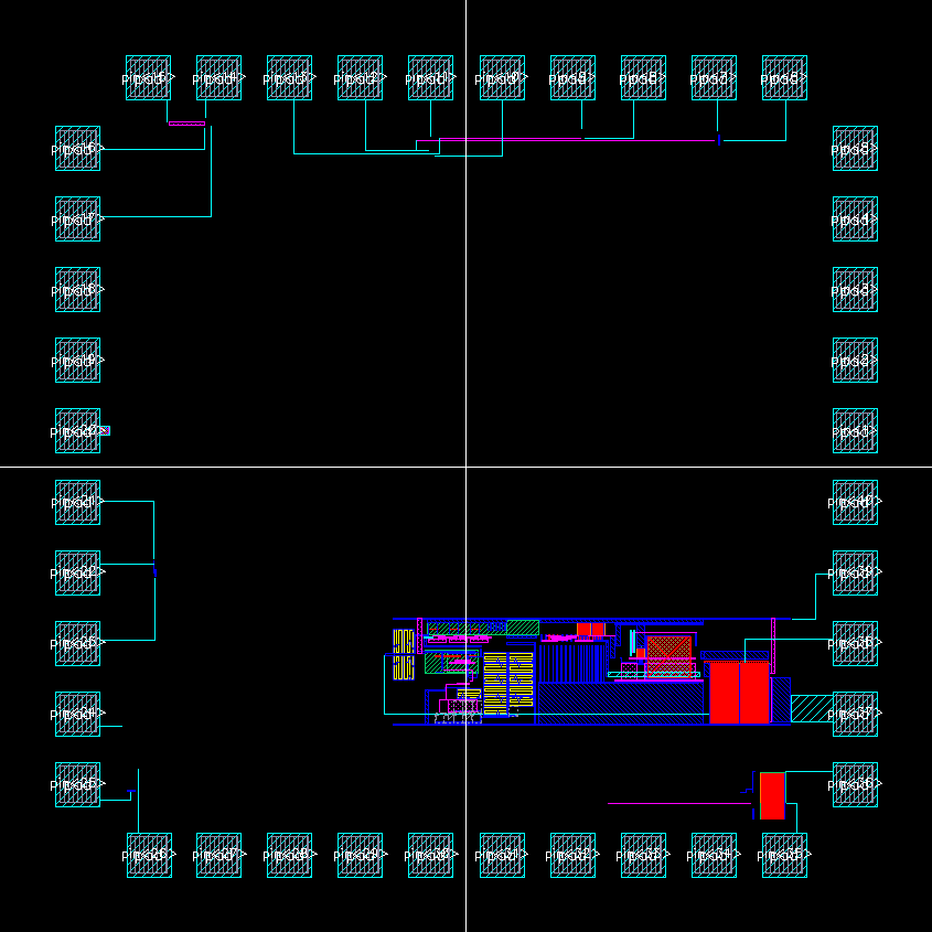
Chip9_f23 Master Layout
Zoomed Views With Device Locations
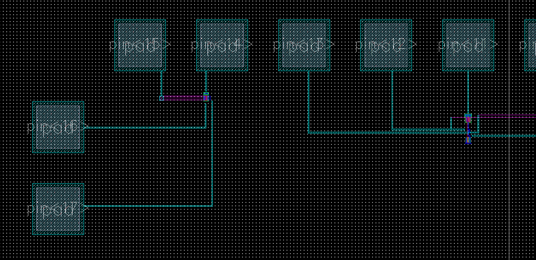
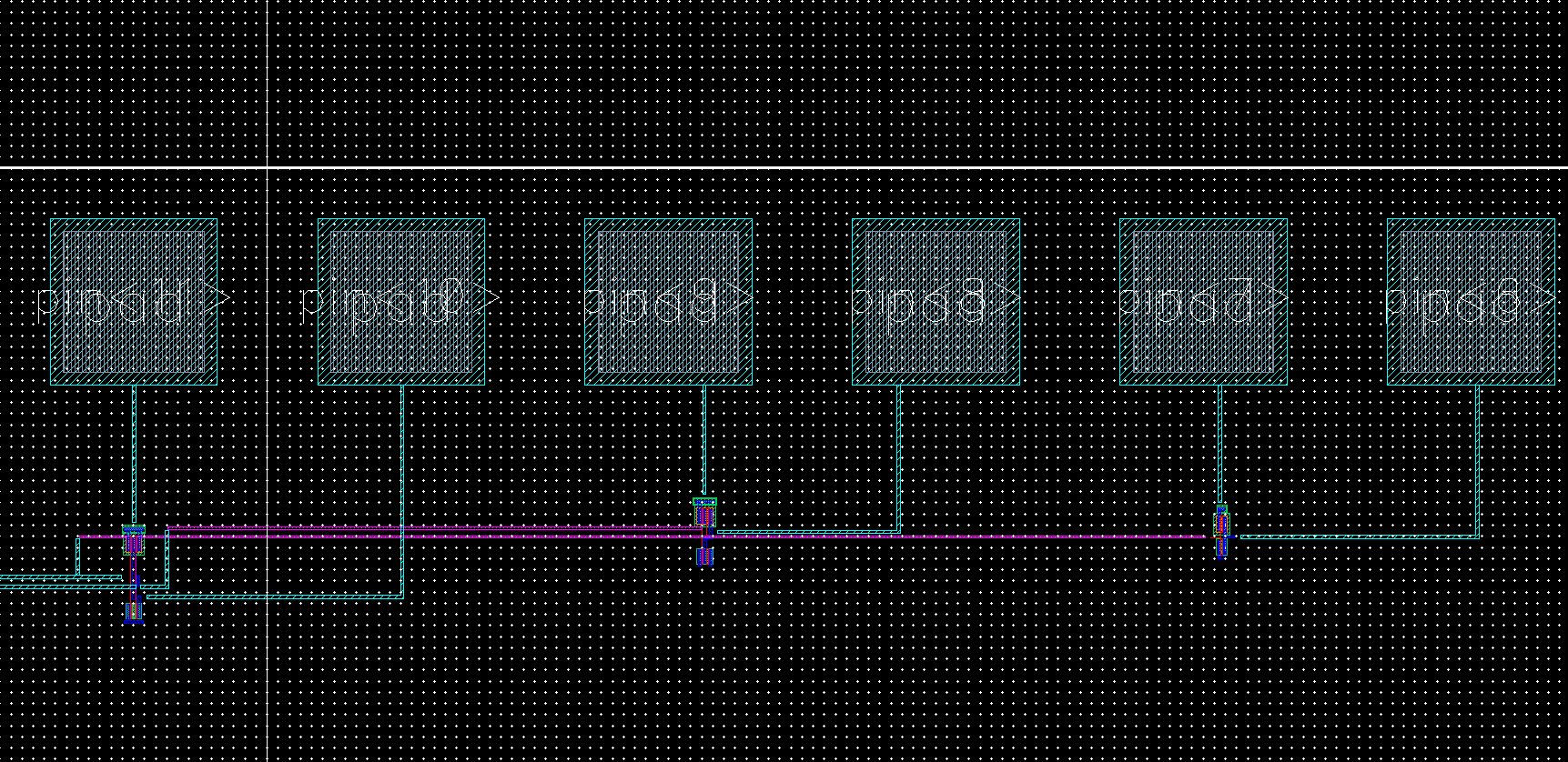
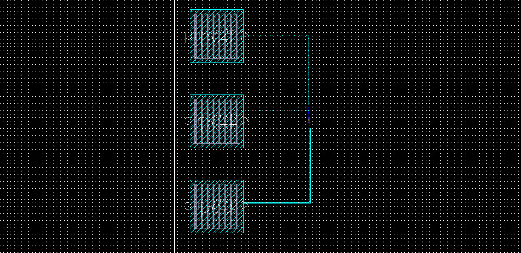
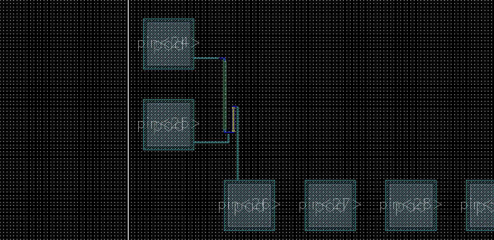
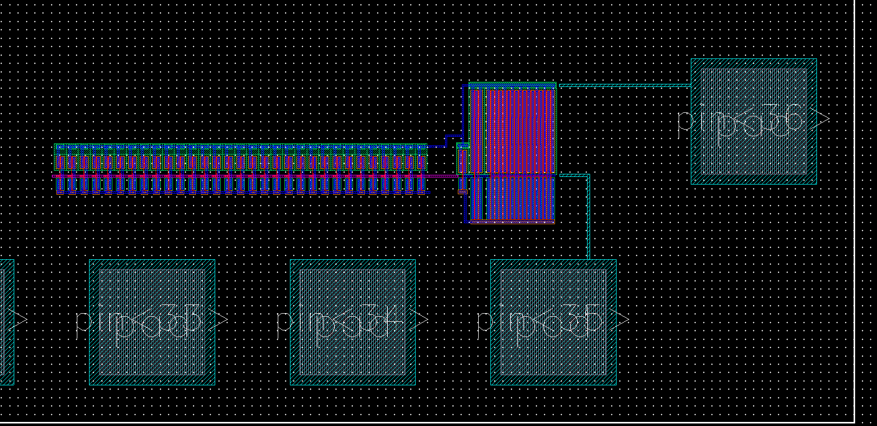
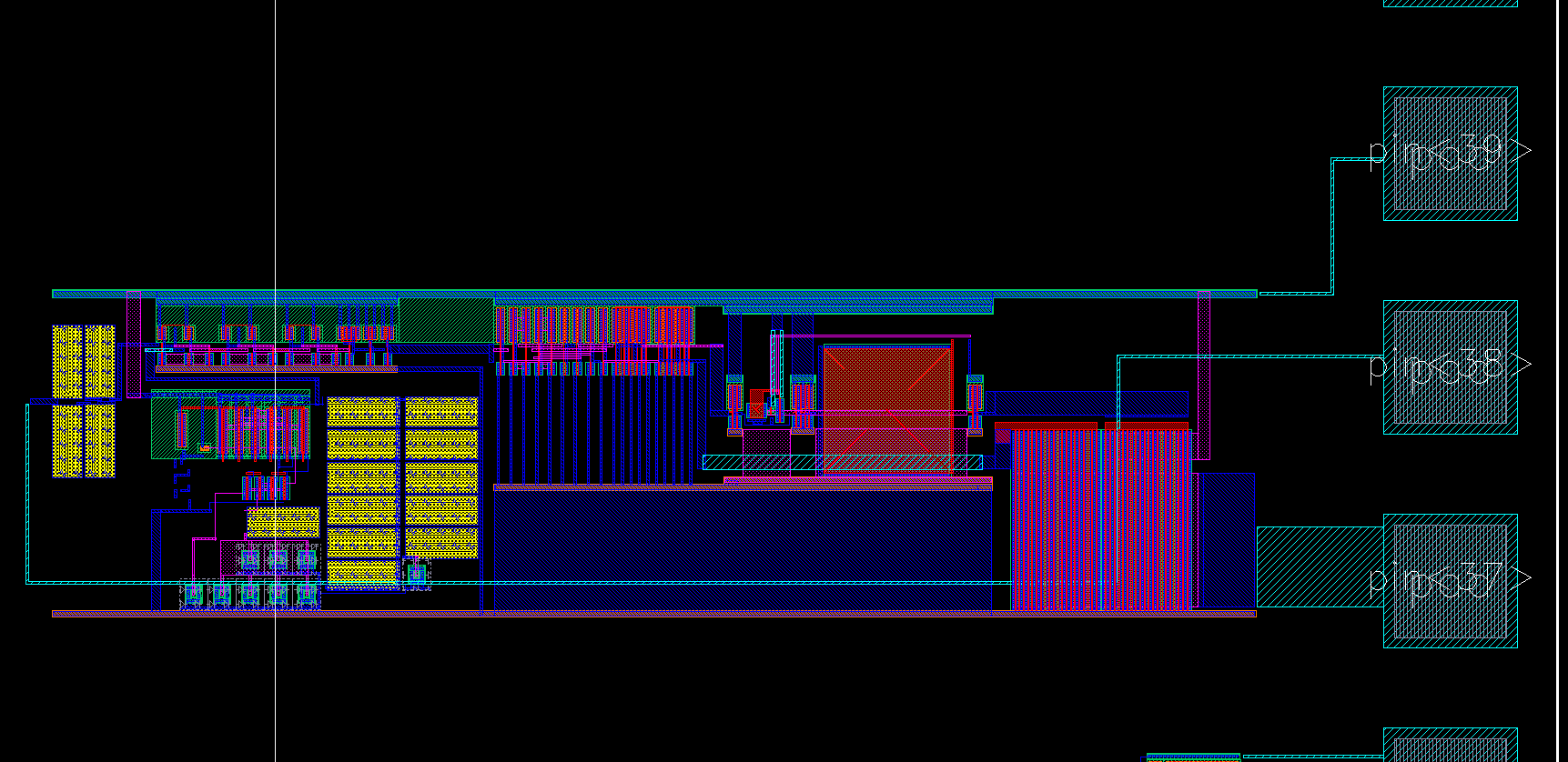
Zoomed Views of Chip9_f23
Chip9_f23 Testing Procedure
All of these devices where tested prior in other labs can can be located here:
- Buck Switching Power supply
- 12/6 Inverter
At any point in the testing procedure Pin 20 can be disonnected at any moment disabling all functionality of the chip and internal devices.
This concludes the testing procedure.