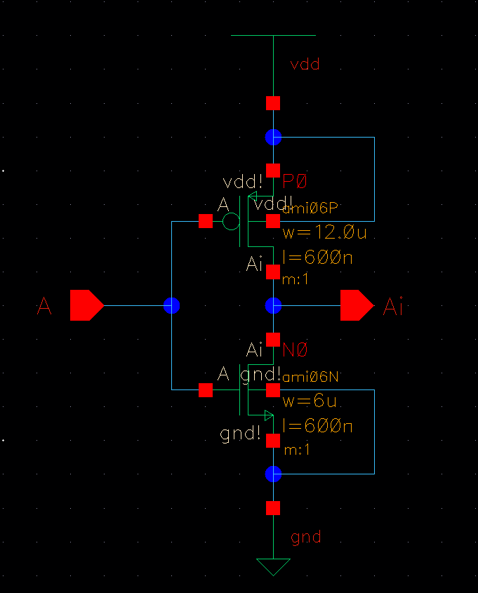
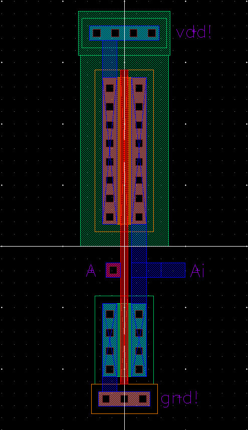
This lab will focus on the design, layout, and simulation of CMOS inverters of two distinct sizes
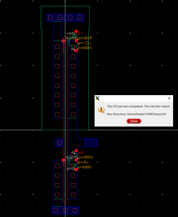
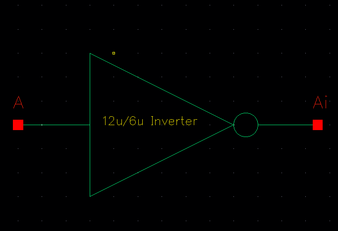
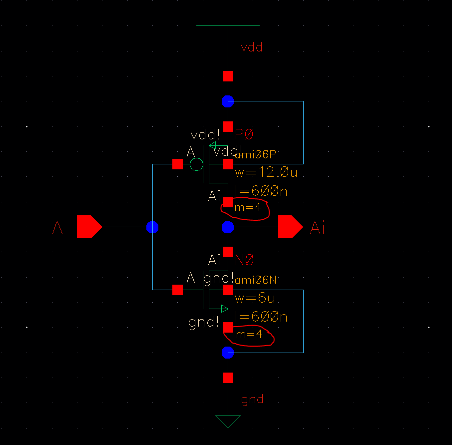
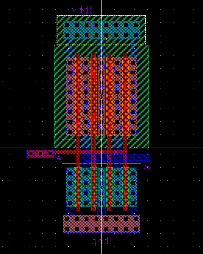
1.) Design a 12u/6u CMOS inverter schematic with corresponding layout and symbol
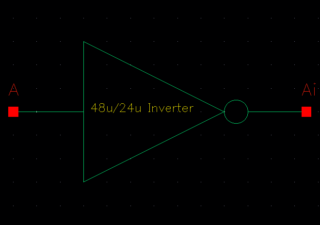
2.) Design a 48u/24u CMOS inverter schematic with corresponding layout and symbol
3.) Design a testing schematic to drive a 100fF, 1pF, 10pF, and 100pF capactior for each inverter, and comment on the results
4.) Perform the simulations above again using the Cadence UltraSim simulator
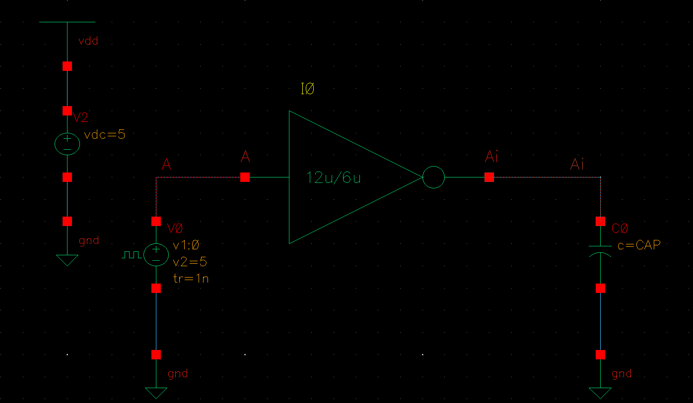
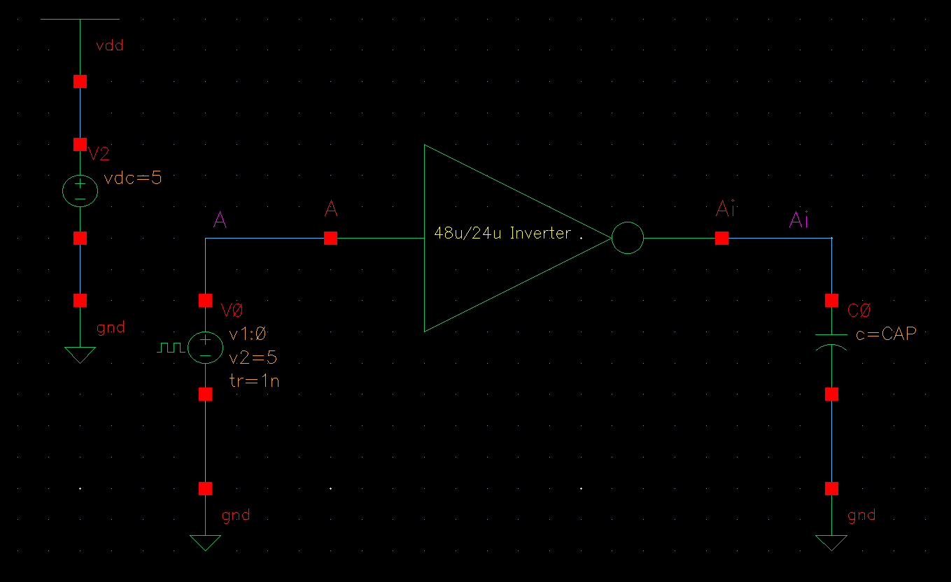
Figure
9(Left 12u/6u), Figure 10(Right 48u/24u): testing schamtics for each
inverter design showing the variable CAP which will be varied through
parametric analysis
Each design was simulated using parametric analysis from 100fF to 100pF in 10pF steps to coner all values in one single simulation. This method produces a cleaner outcome with all values displayed on one graph. See the results below for each inverter.
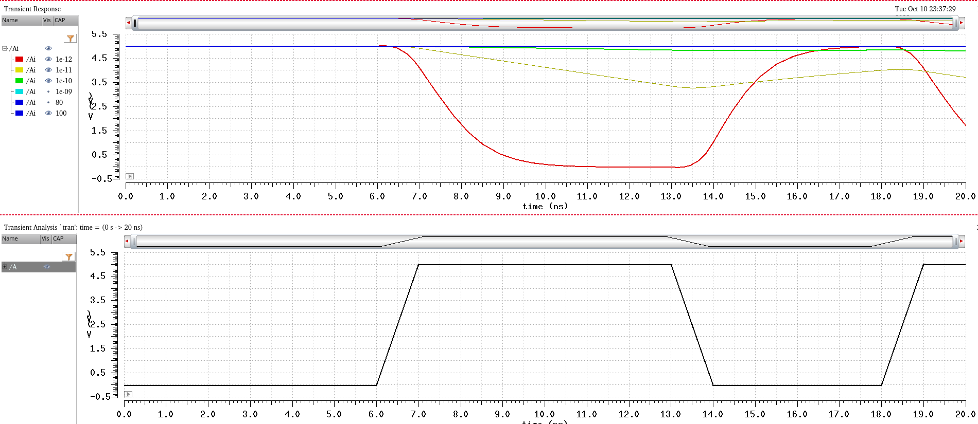
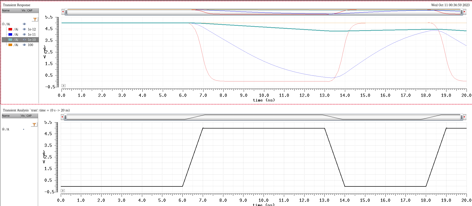
Figure 11(Left 12u/6u), Figure 12(Right 48u/24u): simulation results for each inverter showing a varied capacitance through parametric analysis
4.) UltraSim Simulation
The final step involves performing the same simulations above in the Cadence UltraSim environment.
This can be perfomed by navigating to the Setup -> Simulator/Directory/Host and selecting UltraSim.
NOTE: model libraries for each PMOS and NOMS device needed to be added again.
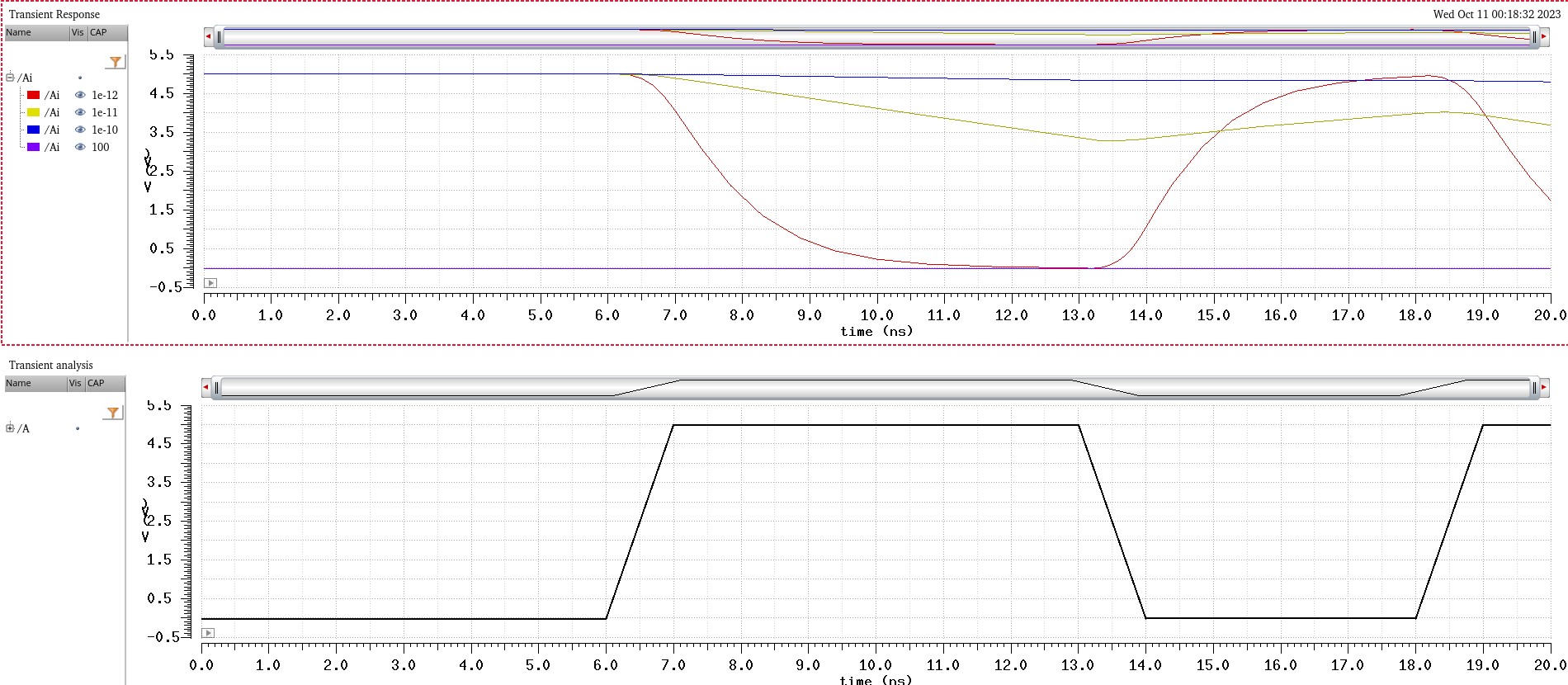
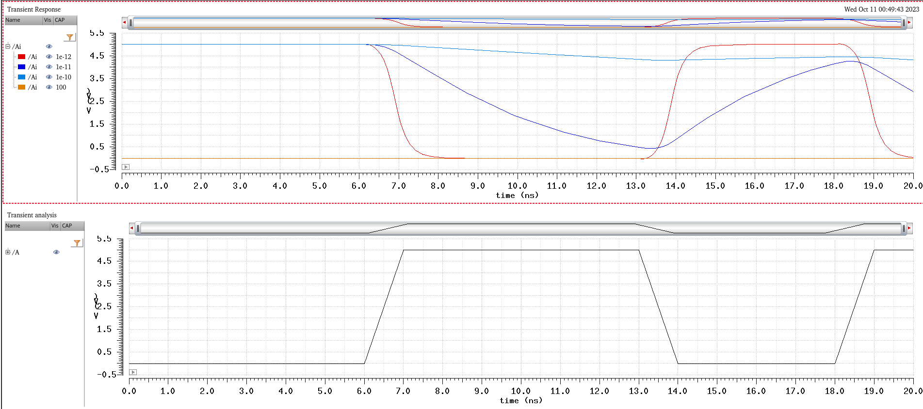
Figure 13(Left 12u/6u), Figure 14(Right 48u/24u): UltraSim simulation varying load capacitance from 100fF-100pF
Conclusion
After reviewing each simulation's results it is clear that the larger 48u/24u inverter size performs far better overall as capacitance values increased.
Each device performed similarily under a very low load of 100fF but as the load increased the switching time for the output was far faster for the larger inverter and this design would be of greater value if switching speed at a higher load was desired. In the domain of high speed logic design, the larger inverter would be the best performance choice, but also comes with trade offs of requiring more current and chip size to operate efficiently.
As with all previous labs, material, simulations, layouts ad results were backed up using .zip files and my personal Google Drive