- This lab will focus on the design, layout and simulation of 2-input NAND & XOR gates in CMOS topology. These gates will then be used to design, layout and simulate a 2-bit full adder.
Pre-Laboratory Procedure
- As with all previous labs, reports, and supporting documents were backed up using .zip files and my personal Google Drive
- Tutorial 4 was completed and lab coumentation was reviewed in its entirety to prepare for the lab instruction
Laboratory Objectives
All objectives should be completed using a standard cell method so all vdd! and gnd! connections align
1.) Draft a schematic a 2-input 6u/6n sized NAND gate in CMOS topology
- provide schematic, layout, symbol views and simulation results proving accurate device operation
2.) Draft a schematic a 2-input 6u/6n sized XOR gate in CMOS topology
- provide schematic, layout, symbol views and simulation results proving accurate device operation
3.) Combine the XOR and NAND gates produced above to build a static full-adder circuit in CMOS topology
- provide schematic, layout, symbol views and simulation results proving accurate device operation
- full adder inputs/outputs should be on metal1 or metal2
Laboratory Procedure
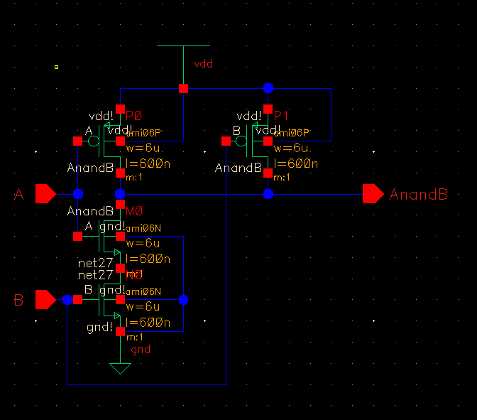
Design of 6u/6n NAND Gate
First I'll begin with a schematic and symbol for the NAND gate, then move on to the layout and simulation
Figure 1: Schematic for NAND gate
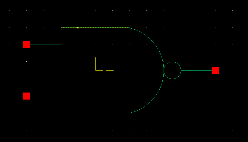
Figure 2: Symbol for NAND gate
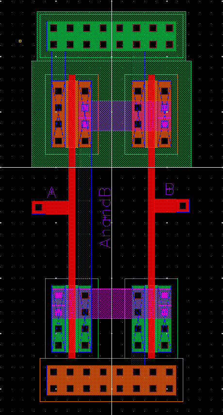
Figures 3 (Left) : Layout for NAND Gate (DRC)
Figure 4(Right) : Extracted views for NAND Gate
The NAND gate will now be simulated using a 5v pulse input and 5V vdd
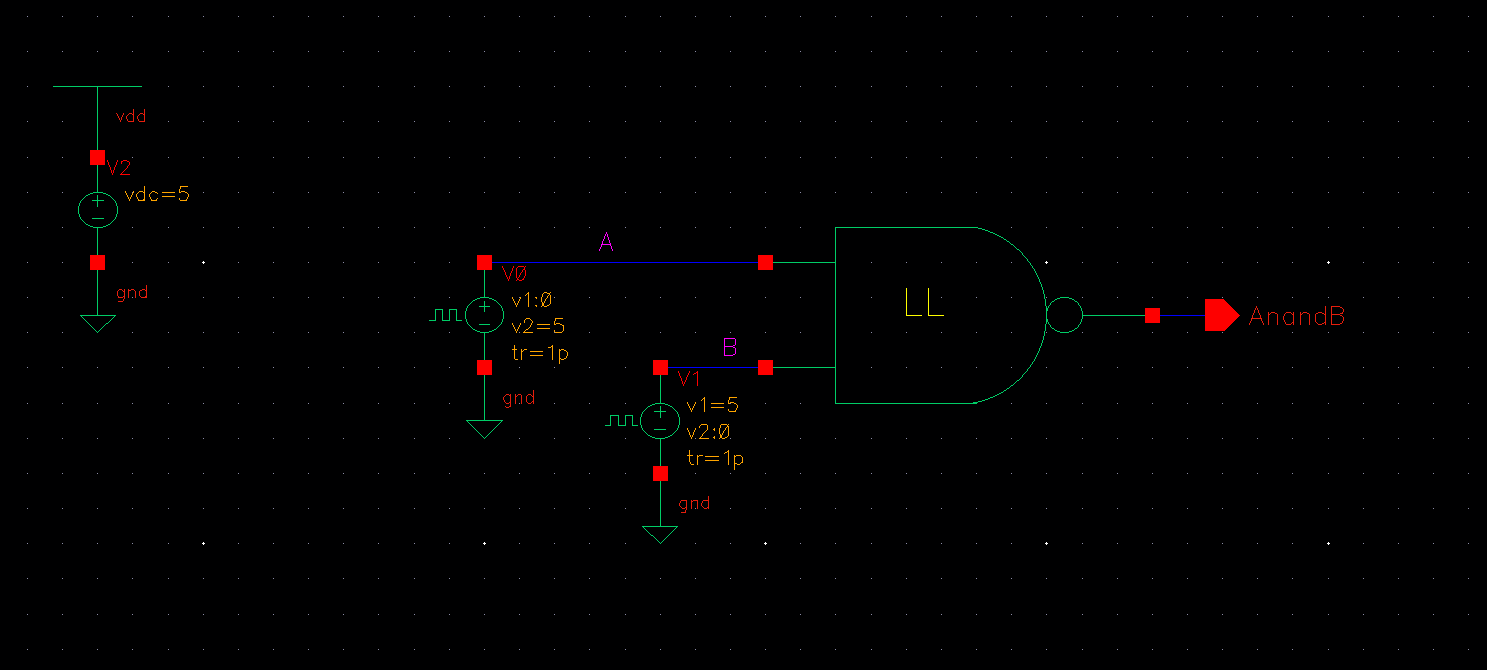
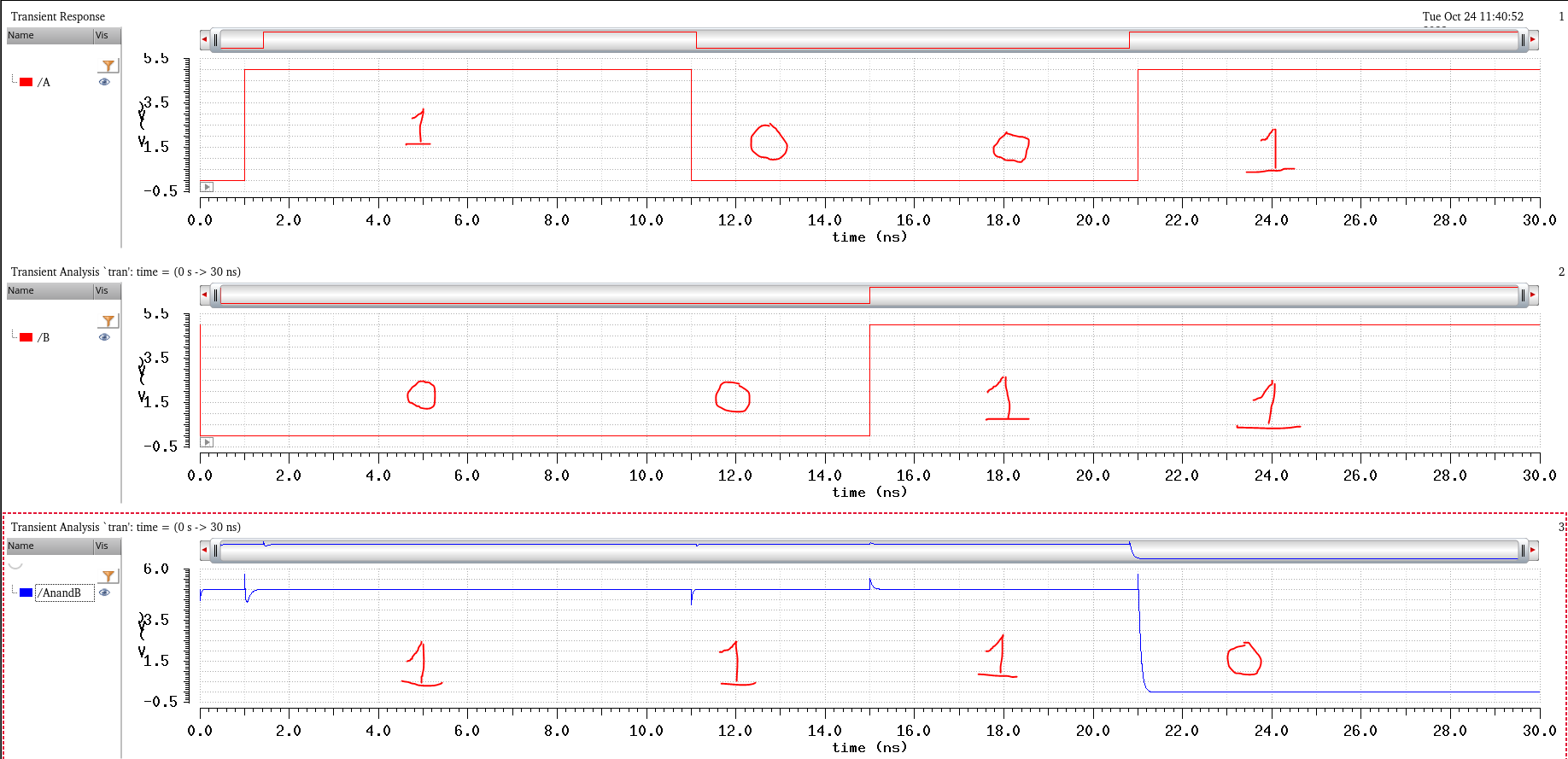
Figure 6: NAND Gate simulation results showing proper device operation
Design of 6u/6n XOR Gate
Again I will begin with a schematic and symbol view, then move on to the layout and extracted with simulation results
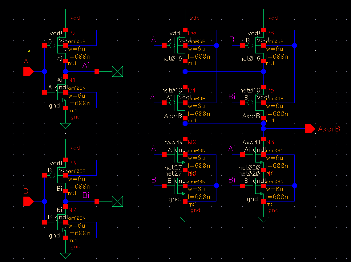
Figure 7: Schematic of XOR Gate
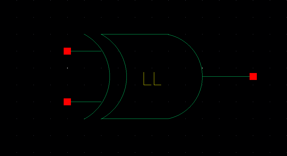
Figure 8: Symbol view of XOR Gate
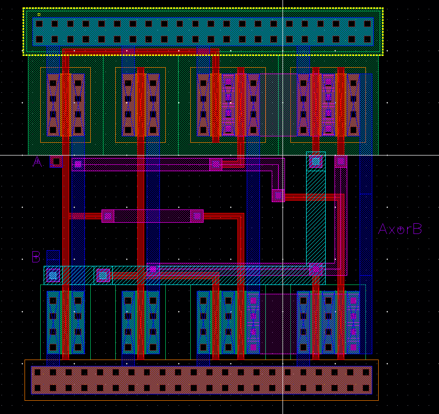
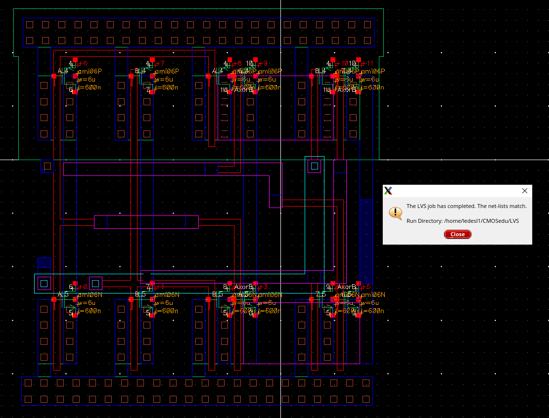
Figure 9(Left): Layout of XOR Gate (DRC)
Figure 10(Right):Extracted views of XOR Gate
The XOR Gate will now be simulated to test functionality using a 5v DC pulse and 5V vdd
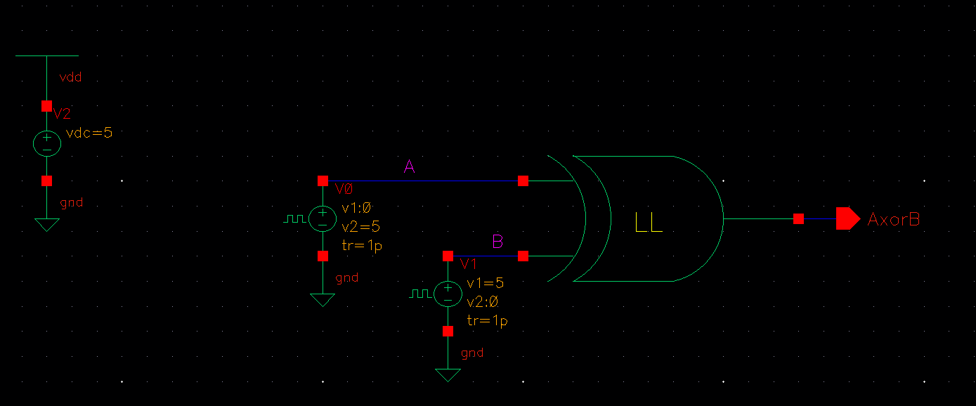
Figure 11: XOR Gate Simulation Circuit
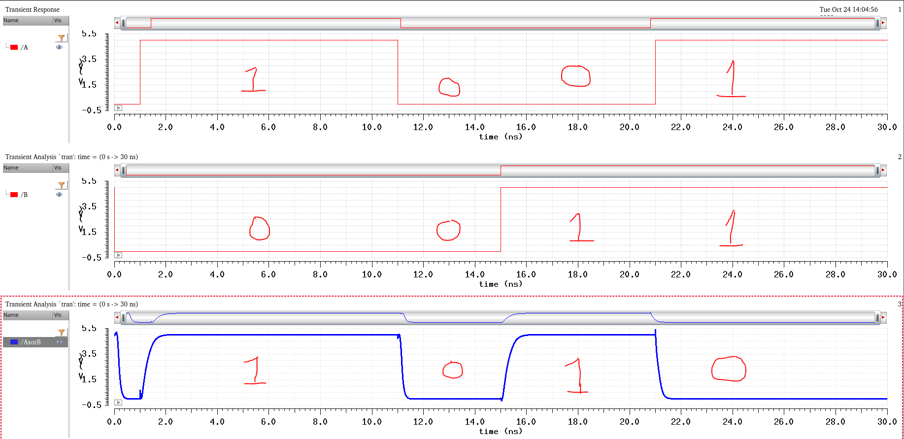
Figure 12: XOR Gate simulation results
NOTE: Reviewing the above simulation and the ones to follow we can see spikes in the output and glitches in the output of the simulation. This is due to brief rise and fall of the input signal. This is caused by the rise or fall when the MOSFET is neither on or off for a very short instance. If the rise and fall time was ideally zero in a true logical transisiton this would eliminate the glitch.
Design of Full-Adder
Combining the two gates built above, I will now combine them to create a static full-adder device. Starting with the same routine of building a schematic, and symbol you can see the results below.
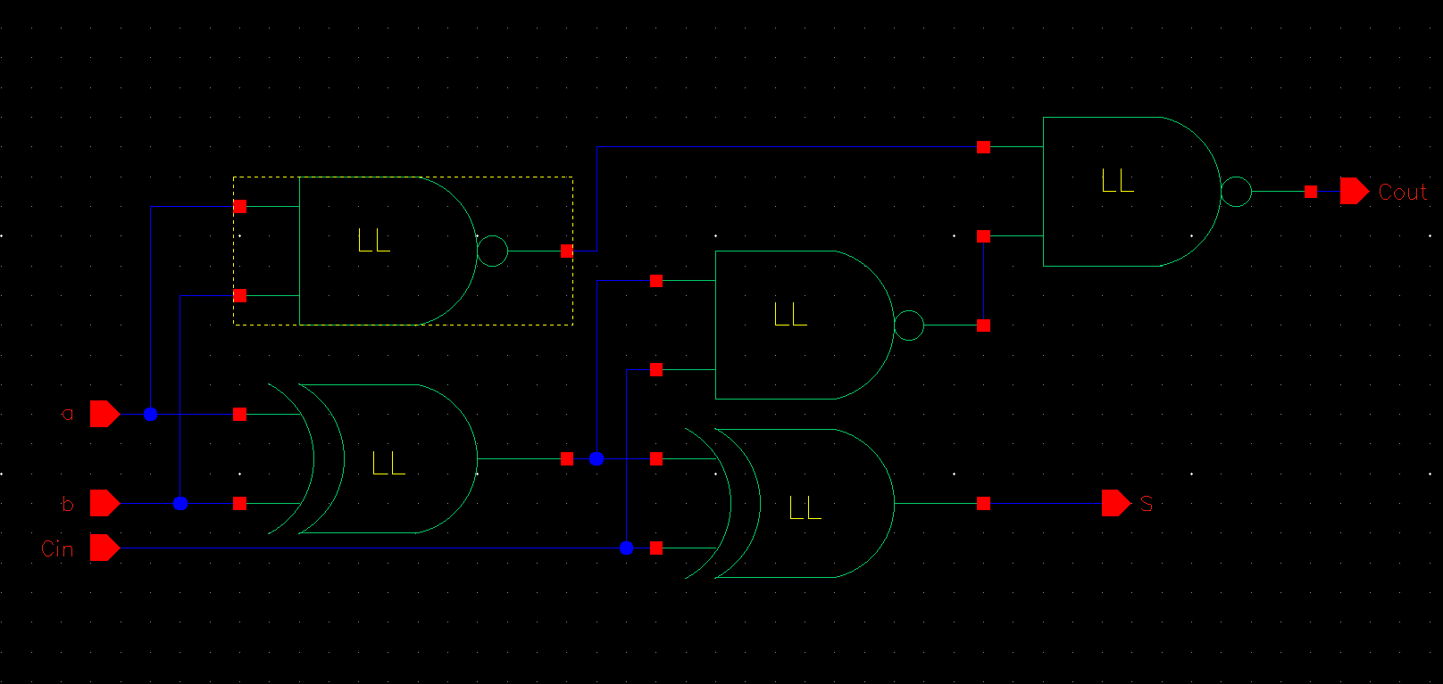
Figure 13: Static full-adder schematic using NAND and XOR gates
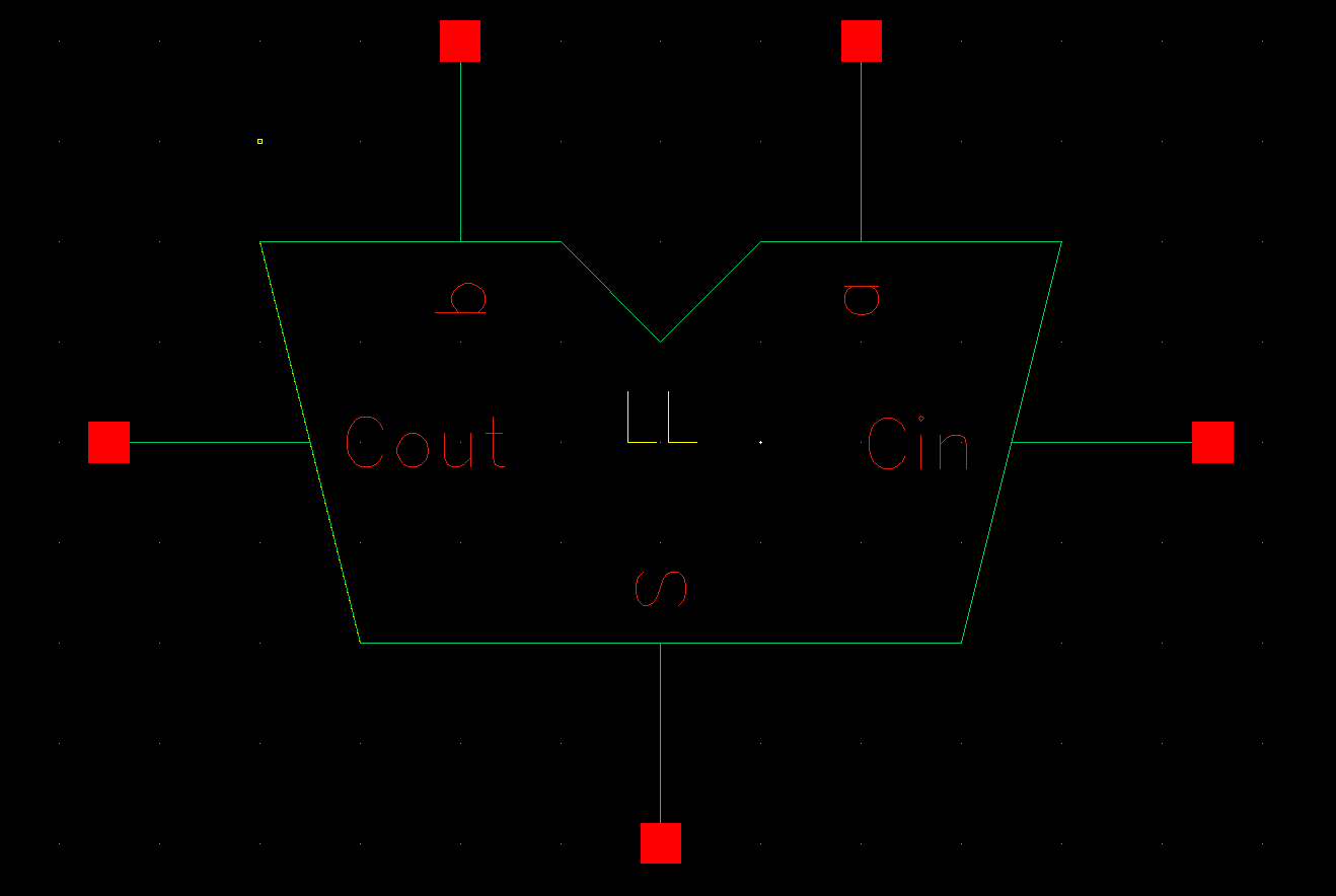
Figure 14: Full-adder symbol view
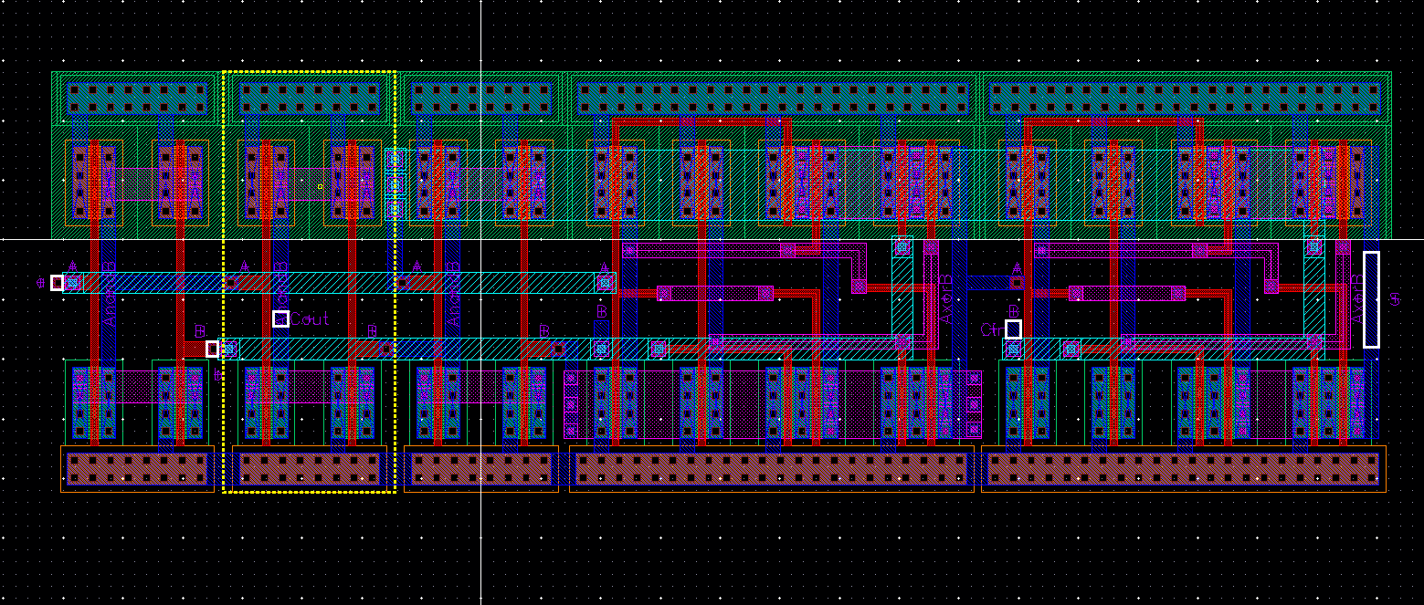
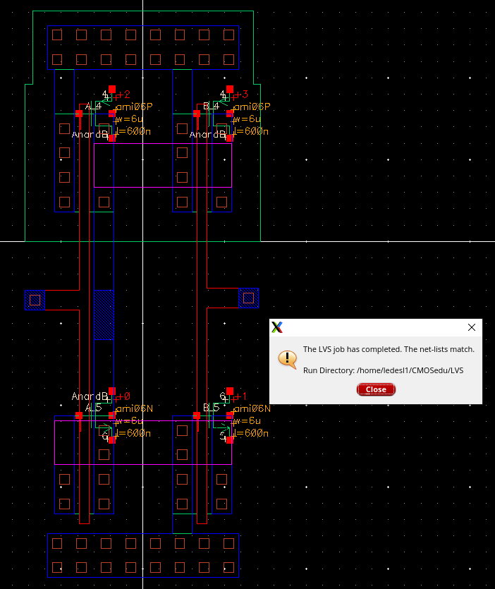
Figure 15: Layout View of full-adder device and (DRC)
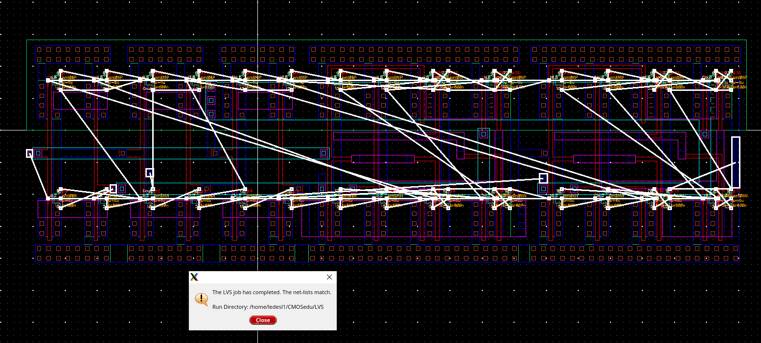
Figure 16: Layout view with LVS confirmation
Finally the Full-Adder will be simulated using 5V DC pulse sources to again provide a logic input to the full-adder and 5V vdd
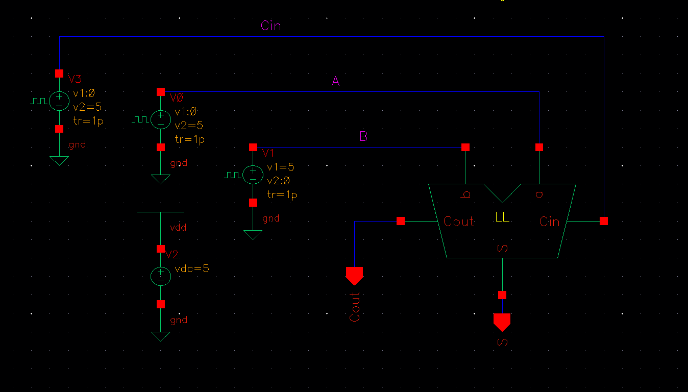
Figure 17: Full-Adder Simulation Circuit
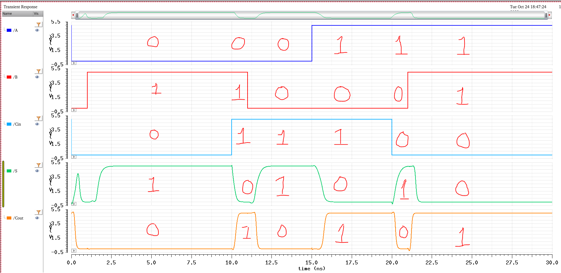
Figure 18: Full-Adder Simulation output showing proper device operation
As with all previous labs, material, simulations, layouts ad results were backed up using .zip files and my personal Google Drive