Digital IC Design - Lab 4 - EE421L
Author: Leonardo Ledesma,
Email: ledesl1@unlv.nevada.edu
September 26, 2023
Lab Description
This
lab will focus on the IV characteristics, layout, and simulation of
PMOS and NMOS devices in the ON Semiconductor Cadence C5 Process.
Pre-Laboratory Procedure
- Before starting this lab, all previous work was backed up using .zip files and my personal Google Drive.
- The lab was read in its entirety to be prepared for instruction after covering all material found in Tutorial 2
Laboratory Objectives
1.) Generate the 4 schematics and simulations below
- 6u/600n NMOS simulating ID v. VDS varying VGS from 0-5V in 1V steps while VDS varies from 0-2V in 1mV steps
- 6u/600n NMOS simulating ID v. VGS for VDS = 100mV where VGS varies from 0-2V in 1mV steps
- 12u/600n PMOS simulating ID v. VSD for VSG varying 0-5V in 1V steps with VSD varying 0-5V in 1mV steps
- 12u/600n PMOS simulating ID v. VSG for VSD = 100mV varying VSG 0-2V in 1mV steps
2.) Lay out a 6u/600n NMOS connecting all 4 terminals to probe pads adjacent to the MOSFET device
- Show DRC confirmation and corresponding schematic with proof of LVS
3.) Lay out a 12u/600n PMOS connecting all 4 terminals to probe pads adjacent to the MOSFET device
- Show DRC confirmation and corresponding schematic with proof of LVS
Laboratory ProcedureThis
lab begins with creating the testing schematics with probe pads for
each NMOS and PMOS device along with a symbol for each. Below you can
see the results of each
PMOS and NMOS device circuit and thier respective symbol created using Cadence Design software.
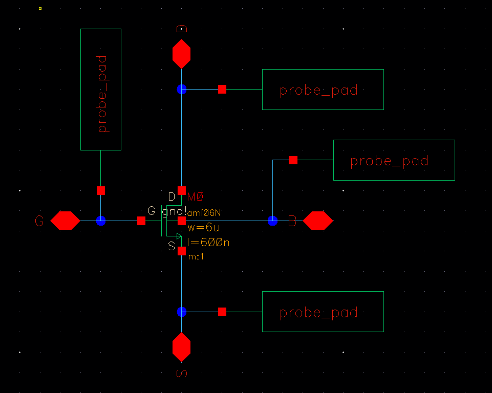
Figure 1: NMOS schematic with pads
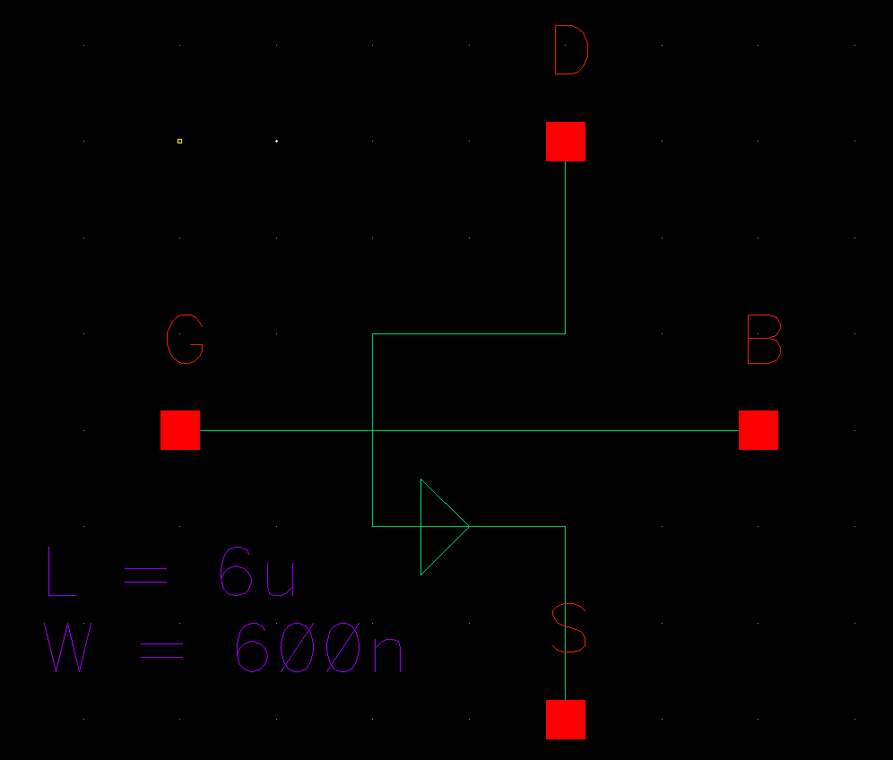
Figure 2: NMOS Symbol
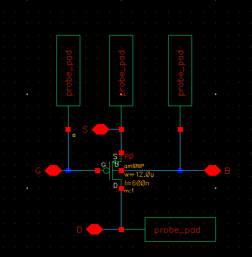
Figure 3: PMOS schematic with pads
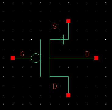
Figure 4: PMOS Symbol
Simulations
A series of simulations will now be performed to obtain the appropriate IV cruves for each device.
NMOS Device - ID v. VDS
- VGS will vary from 0-5V in 1V steps while VDS sweeps 0-5V in 1mV steps
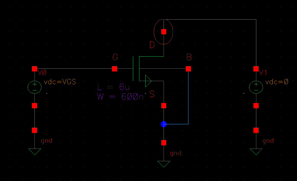
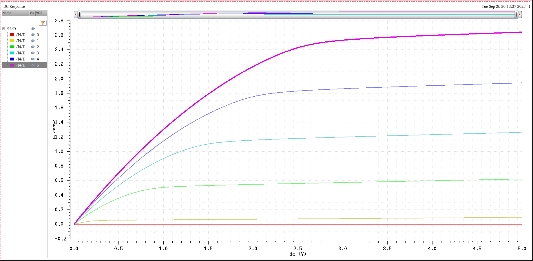
Figure 5a (left): NMOS Simulation circuit
Figure 5b (right) Results simulating ID v. VDS
NMOS Device - ID v. VGS
- VDS = 100mV while VGS is swept from 0-2V in 1mV steps
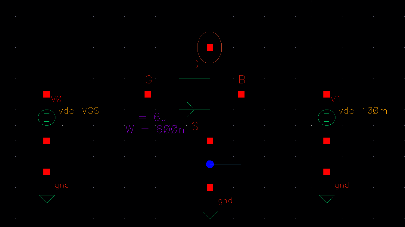
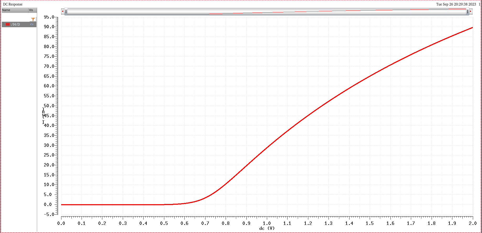
Figure 6a (left): NMOS Simulation circuit
Figure 6b (right) Results simulating ID v. VGS
PMOS Device - ID v. VSD
- VSG is swept from 0-5V in 1V steps with VSD varying 0-5V in 1mV steps
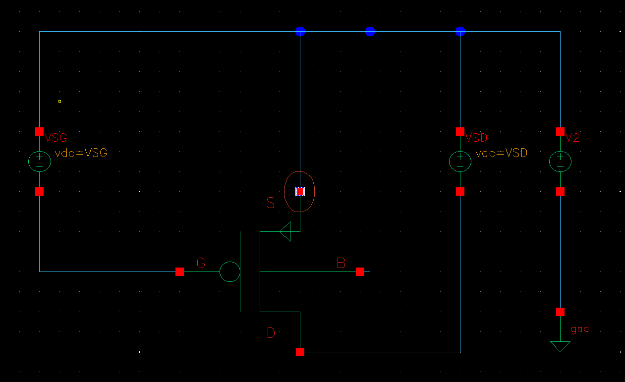
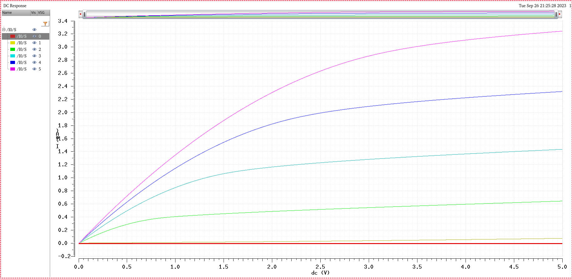
Figure 7a (left): PMOS Simulation circuit
Figure 7b (right) Results simulating ID v. VSD
PMOS Device - ID v. VSG
- VSD = 100mV varying VSG 0-2V in 1mV steps
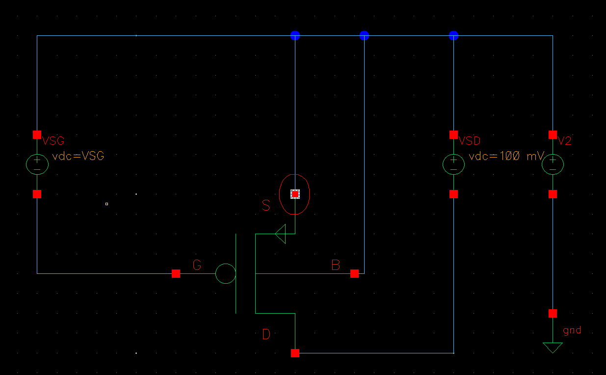
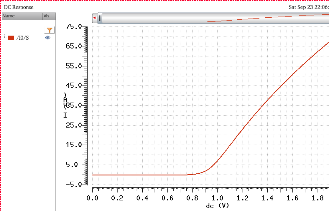
Figure 8a (left): PMOS Simulation circuit
Figure 8b (right) Results simulating ID v. VSG
NMOS 6.0um / 600nm Layout
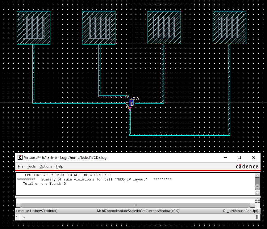
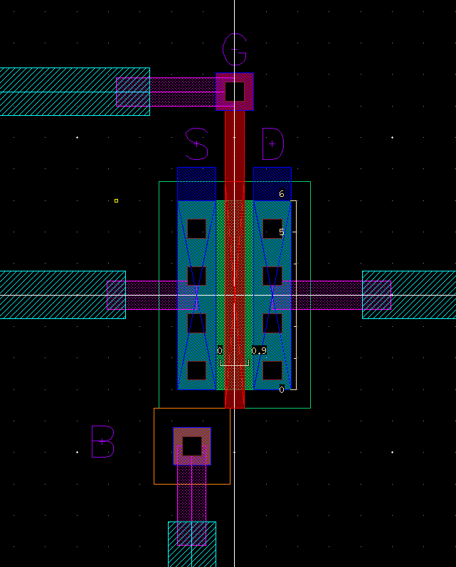
Figure 9a: NMOS layout showing probe pads and DRC confirmation
Figure 9b: Zoomed in NMOS to show connections
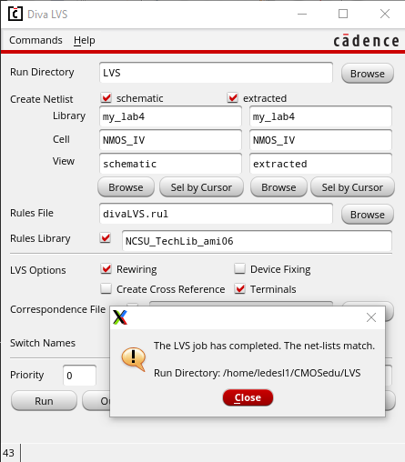
Figure 10: NMOS LVS confirmation
PMOS 12.0um / 600nm Layout
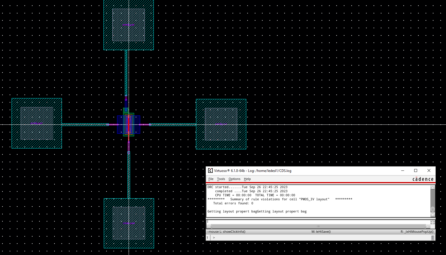
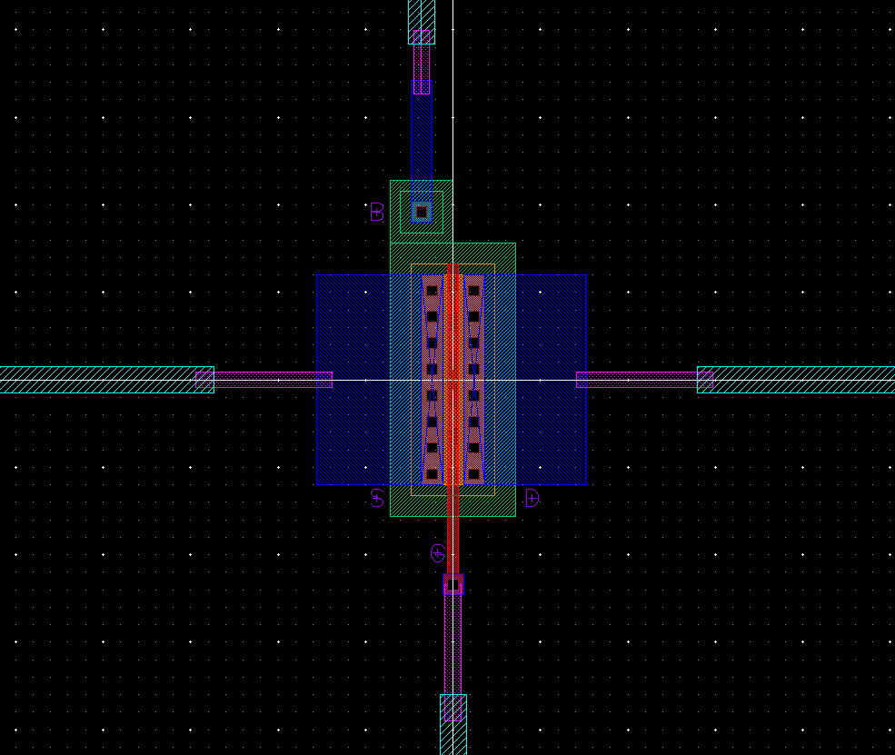
Figure 11a: PMOS layout showing probe pads and DRC confirmation
Figure 11b: Zoomed in PMOS to show connections
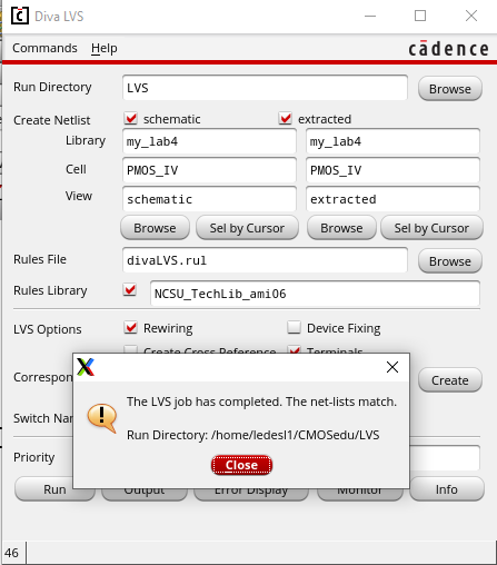
Figure 11c: PMOS LVS confirmation
Backups
As with all prevous labs, work was periodically backed up using .zip files and my personal Google Drive
Return to EE421 Labs


