Test Chip
Overview:
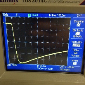
- Circuit is capable of switching high voltages to zero within nanoseconds depending on the number of MOSFETS
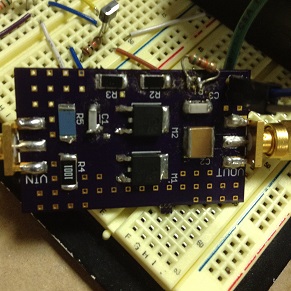
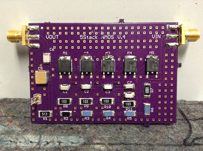
- By stacking five MOSFETs[1] in NMOS configuration, the circuit can switch up to 2.5 kV
- Capacitors are placed in series[2] for a simpler layout
- The same circuit can be modified into a PMOS configuration
- Furthermore, the PMOS configuration can be modified into a C5 process that is capable of switching up to 30 V
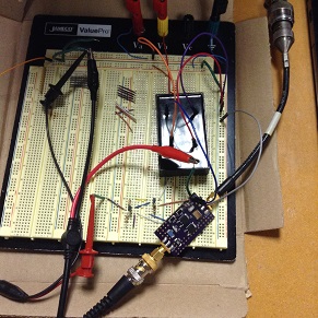
NMOS Tests:
| Test Number | MOSFET | Compeletion |
| Test 1 Test 2 Test 3 Test 4 | STP8NM60 STP8NM60 STP8NM60 STP8NM60 | 04/18/2014 06/09/2014 08/07/2014 12/11/2014 |
PMOS Tests:
| Test Number | MOSFET | Compeletion |
| Test 1 Test 2 | IRF9640 & FQD4P40 IRF9640 | 08/07/2014 12/11/2014 |
Data Sheets:
| Parts | Model Files | Simulation |
N/A N/A | N/A |
References:
[1]Baker, R. Jacob and Johnson, B. P., 1992, "Stacking power MOSFETs for use in high speed instrumentation"
[2]Baker, R. Jacob and Johnson, B. P., 1993, "Series operation of power MOSFETs for high speed, high voltage switching applications"