Lab 8: Generating a Test
Chip Layout for Submission to MOSIS for Fabrication - EE 421L
Authored By: 11/30/15
Jonathan Young Email: youngj1ATunlv.nevada.edu
Jimmy Manone Email: manonej@unlv.nevada.edu
Clinton Bess Email: bessc2@unlv.nevada.edu
Octavio Gonzales Email: gonzao1@unlv.nevada.edu
Our chip is: MOSIS_chip2
Lab Description:
• Students will lay out a set of test structures on a chip for manufacture.
Lab Requirements:
Your chip should include the following test structures:
• One up/down counter with clear
_ The outputs of your counter should be buffered before connecting to a pad
• A 31-stage ring oscillator with a buffer for driving a 20 pF off-chip load
• NAND and NOR gates using 6/0.6 NMOSs and PMOSs
• An inverter made with a 6/0.6 NMOS and a 12/0.6 PMOS
• Transistors, both PMOS and NMOS, measuring 6u/0.6u where all 4 terminals of each device are connected to bond pads (7 pads + common gnd pad)
_ Note that only one pad is need for the common gnd pad. This pad is used to ground the p-substrate and provide ground to each test circuit
• Using the 25k resistor laid out below and a 10k resistor implement a voltage divider (need only 1 more pad above the ones used for the 25k resistor)
• A 25k resistor implemented using the n-well (connect between 2 pads but we also need a common gnd pad)
• Whatever else you would like to fabricate to use the remaining pins on the chip
• Feel free to "sign" the chip or add a graphic (see the bottom of this webpage). Copy the final, DRC and LVS clean cell you want to fabricate, and then add the graphic since the graphic won't DRC
• Also note that you can reduce the number of pins needed by sharing some of them (two resistors, for example, only need 3 pins)
All of the design files associated with this lab can be downloaded: MOSIS_chip2.zip.
Experimental Results:
We made use of both the analog and digital pads given to us so that all inputs, and outputs were buffered. This ensures that getting signals off chip, and on chip will take minimal effort for the user whom should not have to worry about an input signal being slightly non-ideal.
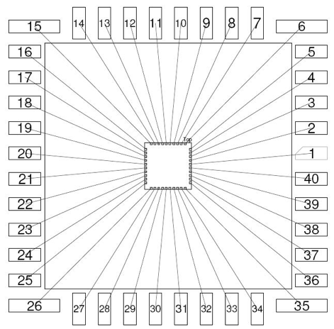
Figure 1: This is the pad frame where all the circuits are connected together. Below is a table that lists which circuits the pins are connected to.
|
Pin: |
Connection: |
Circuit: |
|
0 |
VDD |
Global VDD (not used) |
|
1 |
Power for Counter |
Counter |
|
2 |
Clock Input |
Counter |
|
3 |
Clear |
Counter |
|
4 |
Output <0> |
Counter |
|
5 |
Output <1> |
Counter |
|
6 |
Output <2> |
Counter |
|
7 |
Output <3> |
Counter |
|
8 |
Output <4> |
Counter |
|
9 |
Output <5> |
Counter |
|
10 |
Output <6> |
Counter |
|
11 |
Output <7> |
Counter |
|
12 |
Output |
Ring Oscillator |
|
13 |
Power for Ring Oscillator |
Ring Oscillator |
|
14 |
Input<1> - Into 25kΩ |
Voltage Divider |
|
15 |
Input<2> - Out of 25kΩ (tap) |
Voltage Divider |
|
16 |
Gate |
PMOS |
|
17 |
Source |
PMOS |
|
18 |
Drain |
PMOS |
|
19 |
Power for PMOS |
PMOS |
|
20 |
Ground |
Global Ground |
|
21 |
Gate |
NMOS |
|
22 |
Source |
NMOS |
|
23 |
Drain |
NMOS |
|
24 |
Power for NMOS |
NMOS |
|
25 |
Output |
NAND |
|
26 |
Input<1> |
NAND |
|
27 |
Input<2> |
NAND |
|
28 |
Power for NAND |
NAND |
|
29 |
Output |
NOR |
|
30 |
Input<1> |
NOR |
|
31 |
Input<2> |
NOR |
|
32 |
Power for NOR |
NOR |
|
33 |
Input |
Inverter |
|
34 |
Output |
Inverter |
|
35 |
Power for Inverter |
Inverter |
|
36 |
NOT USED |
NA |
|
37 |
NOT USED |
NA |
|
38 |
NOT USED |
NA |
|
39 |
Up/Down Toggle |
Counter |
Note: All power pins are
separate to prevent one circuit from shorting the others and thus allowing
other circuits to be tested.
Circuits Designers:
_
Counter, Inverter, NAND, and
NOR circuits – Jonathan Young
_
Ring Oscillator – Clinton Bess
_
Transistors (NMOS and
PMOS) – Jimmy Manone
_
Voltage Divider – Octavio Gonzales
Note: Review their lab project
reports for specific functionality of how these devices function and were
setup. Links to their project’s reports can be accessed by clicking the
designer’s respective name.
Schematic:
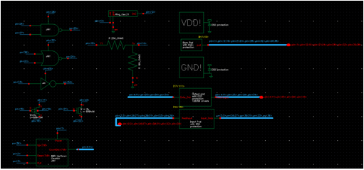
Figure 2: This is the schematic showing all the circuits in the pad frame, including the pin allocation.
Layout:
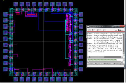
Figure 3: This shows the layout of the circuits with the pad frame and that it passes DRC
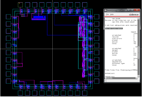
Figure 4: This image shows the extracted layout of the circuit with the pad frame and that it passes LVS.
Instructions for testing:
A global ground is used, so connect pin<20> to ground to test any or all of the following components:
_
Connect the components to the
respective pins above for testing and output, the <#> designates which
output the pin is.
Counter:
_
Pin<11:4> is in order of MSB
to LSB, with pin<4> being the LSB.
_
UP is active high: when UP is high,
the counter counts up, and when UP is low, it counts down.
_
When CLEAR is high, the outputs are
set to 0.
Voltage Divider:
25kΩ resistor:
First connect pin<20> to ground. Then measure between pin<14> and pin<15>.
10kΩ resistor:
Connect pin<20> to ground, then measure between pin<15> and ground, pin<20>.
Voltage Divider:
Connect pin<20> to ground, apply the input voltage to pin<14>, and measure the output between pin<15> and ground, pin<20>.