Generating GDSII and MOSIS information from CMOSedu.com
Information about
the MOSIS University Support Program is found here.
Below are examples
of how to fill out the forms for submitting designs in GDSII format (aka GDS or Stream) for
fabrication through MOSIS in ON Semiconductor's C5
(MOSIS, for some reason, is now calling this B5 but ON still uses C5)
process (500 nm, 3 metal layers, 2 poly layers, see information from ON
here)
To generate a GDSII file
A
GDS file of your chip may be generated in the Electric
CAD system by going to File -> Export -> GDS II (Stream)…
A
GDS file can be read into Electric using File -> Import
-> GDS II
(Stream)…
Here
is an example of how to generate a GDS file using Cadence
IC51 (start, as
above, in the
CIW and File -> Export -> Stream).
A
GDS file can be generated in Cadence
IC61 via the CIW using File -> Export -> Stream (image)
In the NCSU Cadence IC61 setups located in $HOME/ncsu-cdk-1.6.0.beta/lib/NCSU_TechLib_ami06 overwrite the layer map (which is incomplete, a bug in the IC61 beta setups) with NCSU_TechLib_ami06.layermap (a complete layer map of the MOSIS GDS layers).
If the cell you want to fabricate is called CHIP, and it’s in a library
called PxC_CHIP, then here
is how the Stream Out menu is setup (hit Translate to generate the
stream, aka
GDS, file). The
stream (GDS) file is saved in your working directory
To
check that you have generated the GDS file correctly using Cadence
IC51, IC61,
Electric, Silvaco EDA, or whatever layout tool you are using, download KLayout
or OwlVision and compare the layers seen using this tool to the layers seen in the
layout
tool you are using.
To submit a design to
MOSIS
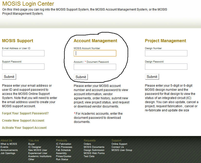
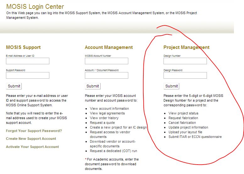
To begin login
to your MOSIS account here.
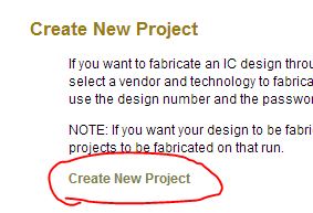
Next create a
new project.
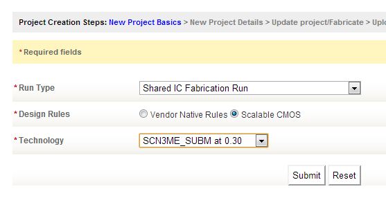
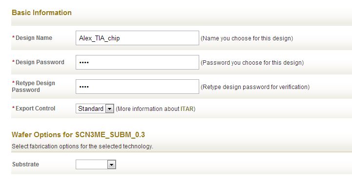
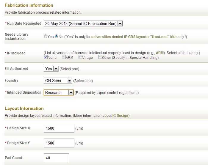
Then fill out
the following (for example).
In general,
it’s okay to specify “Yes” to the “Fill Authorized:” question to help
your chip
meet the minimum
density requirements for CMP. One example where you many not want fill is if you have photodetectors
on you design. Fill on any of the layers may block the light from hitting your photodetector.
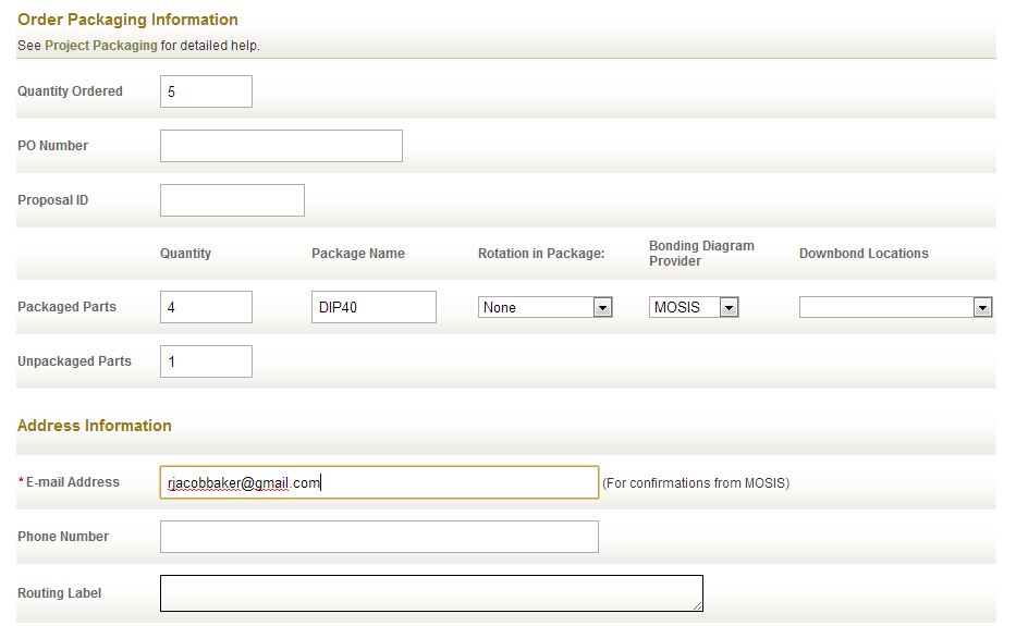
Next fill out
the order information.
The MOSIS
Educational Program (MEP) instructional account provides 5 chips per
submitted
design in
ON’s C5 or
IBM’s 8RF-DM processes (see: http://www.mosis.com/pages/Faqs/faq-education).
All to none of the
5 chips can be
packaged in a 40-pin DIP. If 4 of your designs are to be packaged then
1 should
be specified
in the
unpackaged (bare die) field as seen below.
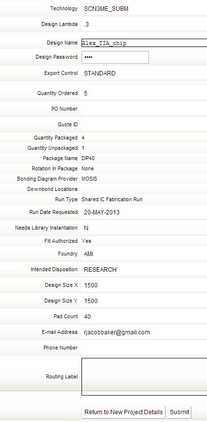
After hitting
the Submit button return to the MOSIS login center here
and enter
the design number you receive in an email
and the design
password you selected above (not
your MOSIS account/document password).
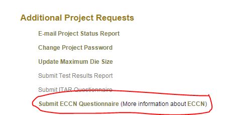
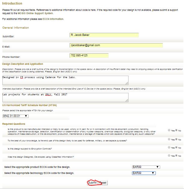
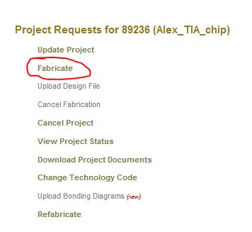
Then select Submit ECCN questionnaire, fill out the form, and then select Fabricate as seen below (go back to the project
management page if needed).
A link to the Harmonized Tariff Schedule, useful in the updated form below, is found here.
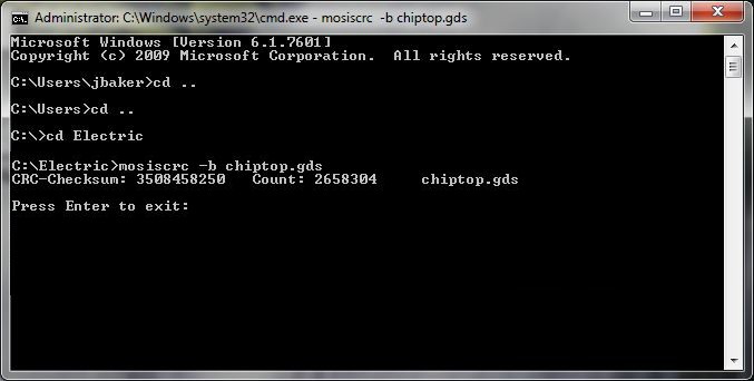
Before we can
submit the GDS file for fabrication we need to download the mosis
crc executable for
determining the
Checksum and
Count here.
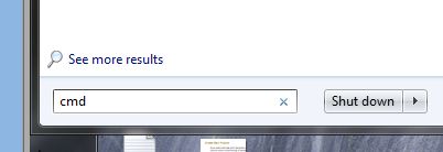
In Windows
Start -> Run -> Cmd
to open a terminal then
navigate to where you saved this executable and the binary
GDS file (e.g.
save both in C:\Electric as seen below).
Then type: mosiscrc -b chiptop.gds where
“chiptop.gds” is the name of the GDS file you want to fabricate.
Notice the output is a
checksum number (first, larger number)
and count (second, smaller number).
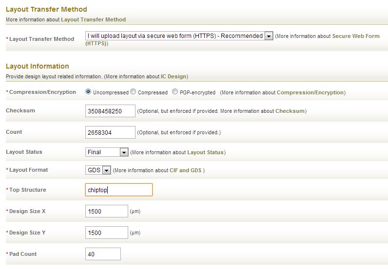
Next fill out
the layout transfer method and information forms seen below.
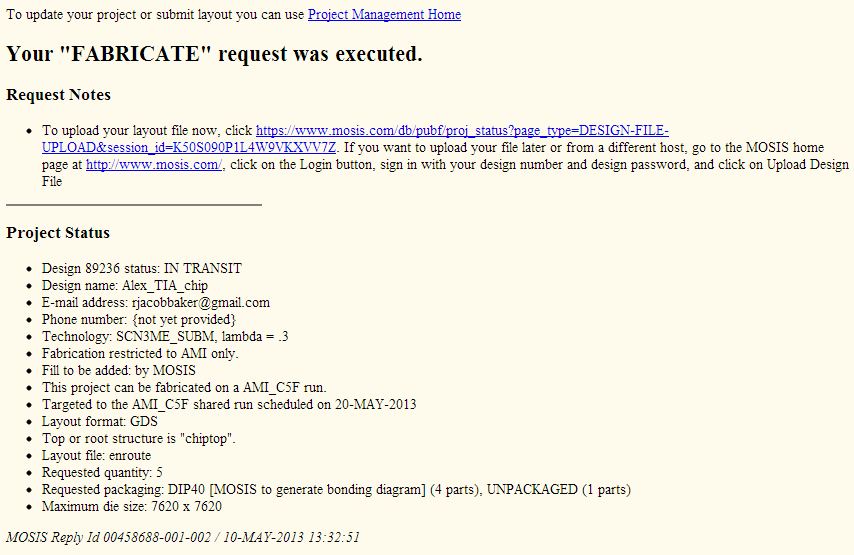
After hitting
the Submit button you will get the following. Click on the link to
upload your
design.
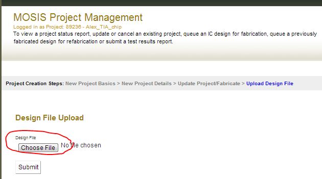
After choosing
the GDS file, here chiptop.gds located in the C:\Electric directory,
and
uploading we get the following.
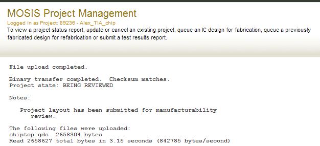
MOSIS will
email you a link to a bonding diagram for the design.
Other emails will
be sent after checking the design (using the checksum and count) and
after the
design is queued for fabrication.
Some
other notes.
- Do not submit chips
with pixilated text or graphics that fail the DRCs.
Below is an example (used as a label on a chip near a bonding pad).
![]()
- An example of a layout
where pixilated text may be okay, because the chip was fabricated in an
older CMOS process, is seen below.
- In a smaller IC
process (e.g., < 500 nm CMOS) a problem with pixilated
text/graphics has to do with chemical-mechanical planarization (CMP)
and clean patterning.
- Crud from the smaller
dimensions of the patterned materials can be generated that interferes
with the CMP process.
- So unless you are
designing in an older process the chip you submit should pass DRCs (no
pictures!)
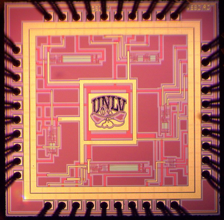
- If
you are fabricating in an older process you can use LinkCAD to convert
images into GDS (e.g., UNLV.gds
and BSU.gds, right click to
Save link as)

CMOS Circuit
Design, Layout, and
Simulation
CMOS Mixed-Signal
Circuit Design