Project I - EE 421L: Digital Integrated
Circuit
Design Laboratory
Generating
a test chip layout for submission to MOSIS for fabrication.
Lab Work
Post-Lab Scope
Below
are the pre-lab deliverables.
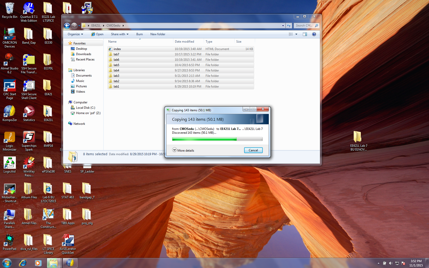
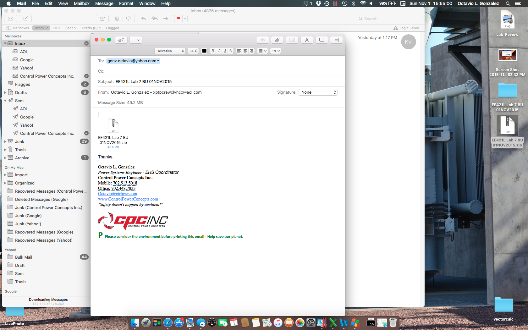
As can be seen, before starting, backing up all the work from the EE421 Lab and Course is required.
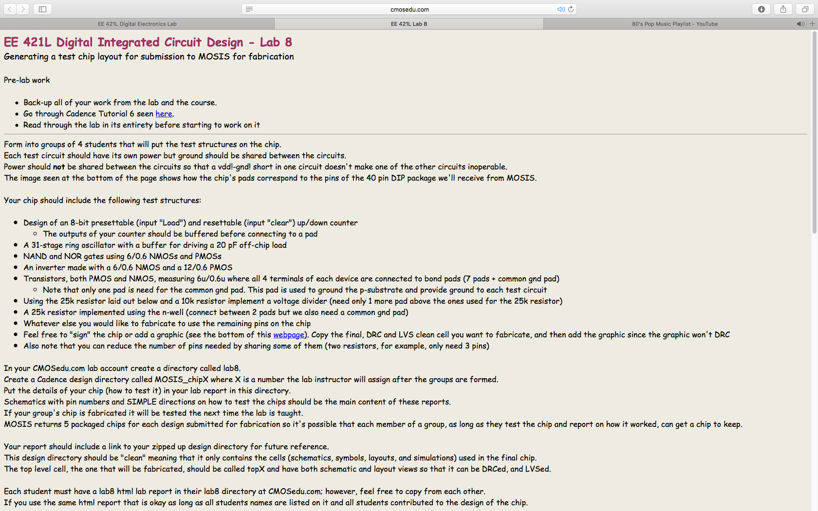
Below is a screenshot of reading through the Lab 8 requirements and scope prior to starting the assignment.
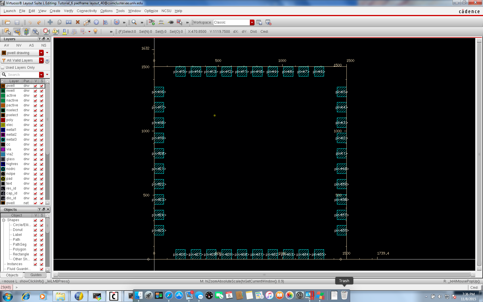
Tutorial 6
As
can be seen below, Tutorial 6 has been completed.
Formation of Groups
The members that form this group are as follows:
Clinton Bess
Jimmy Malone
Jonathan Young
Octavio L. Gonzalez
Post-Lab:
Below are the post-lab deliverables.
The following are are the individual chip test structures and the detailed procedures to verify their operation
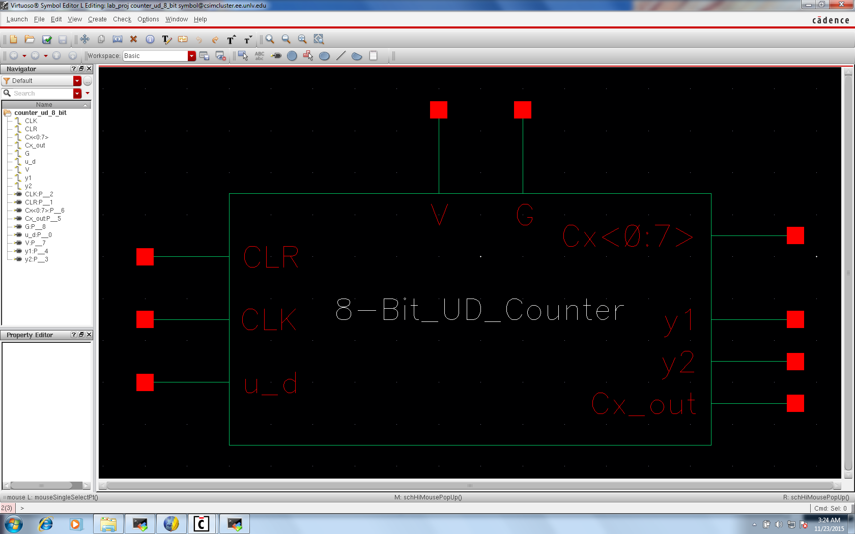
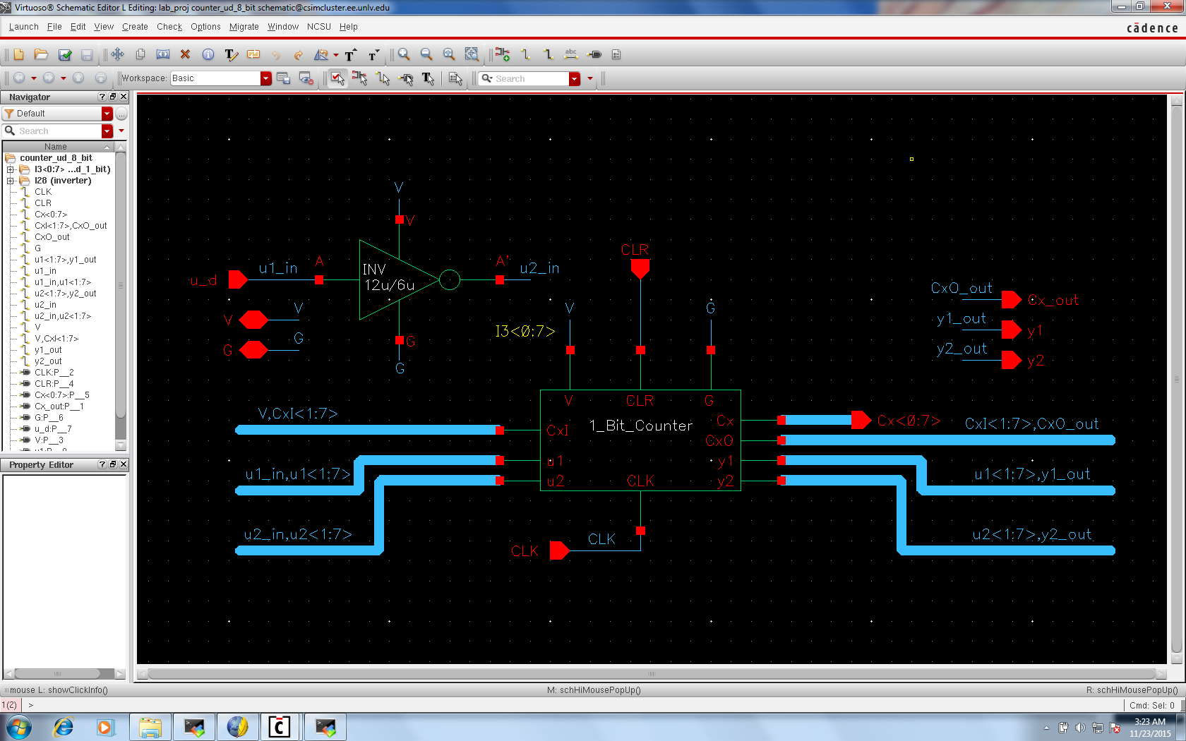
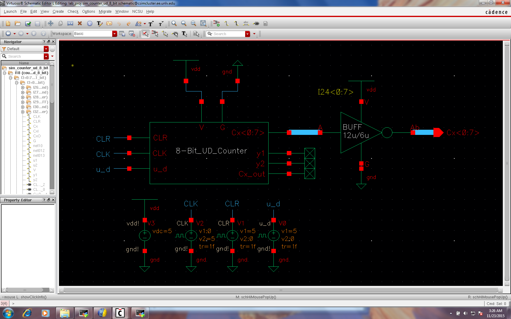
8-Bit Presettable/Resettable Up/Down Counter
Up Down Counter Symbol
Up Down Counter Schematic
Up Down Counter Simulation Schematic
Refer to miscellaneous section of this report for sub-level components and devices that make the 8-bit counter.
Simulation
Reseting with Counting Up and Down
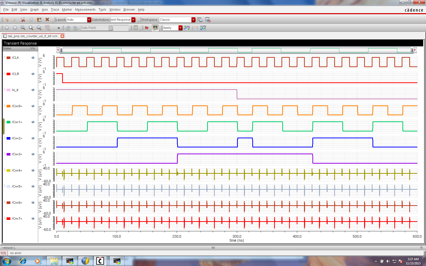
As
can be seen above the clear input sets the counter to zero, after the
signal is lifted the up count initiates then switches to down count accordingly.
Up Down Counter DRC
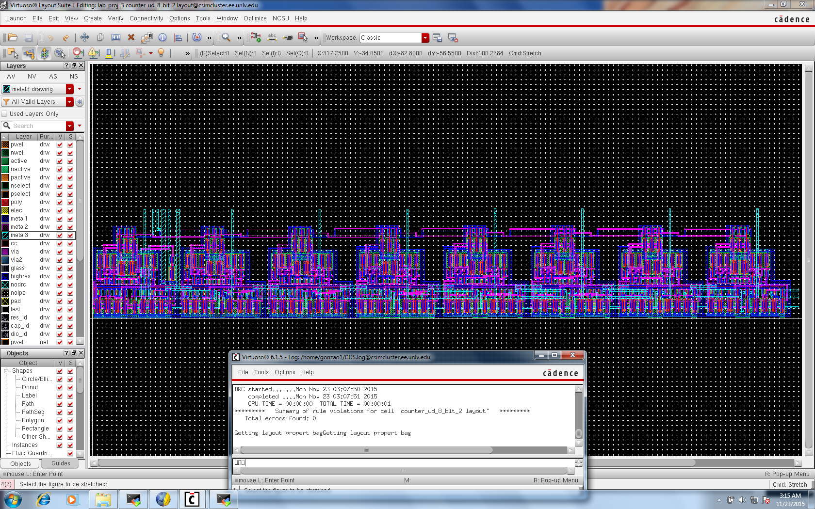
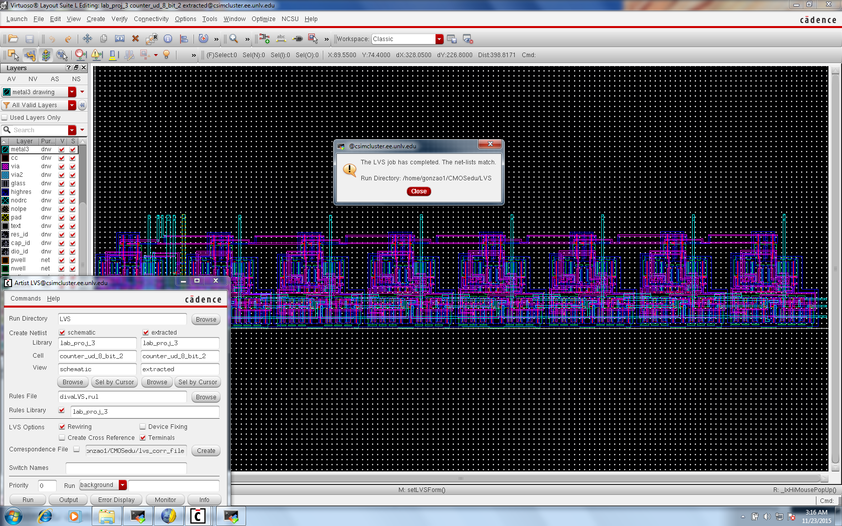
Up Down Counter LVS
31-Stage Ring Oscillator
Ring
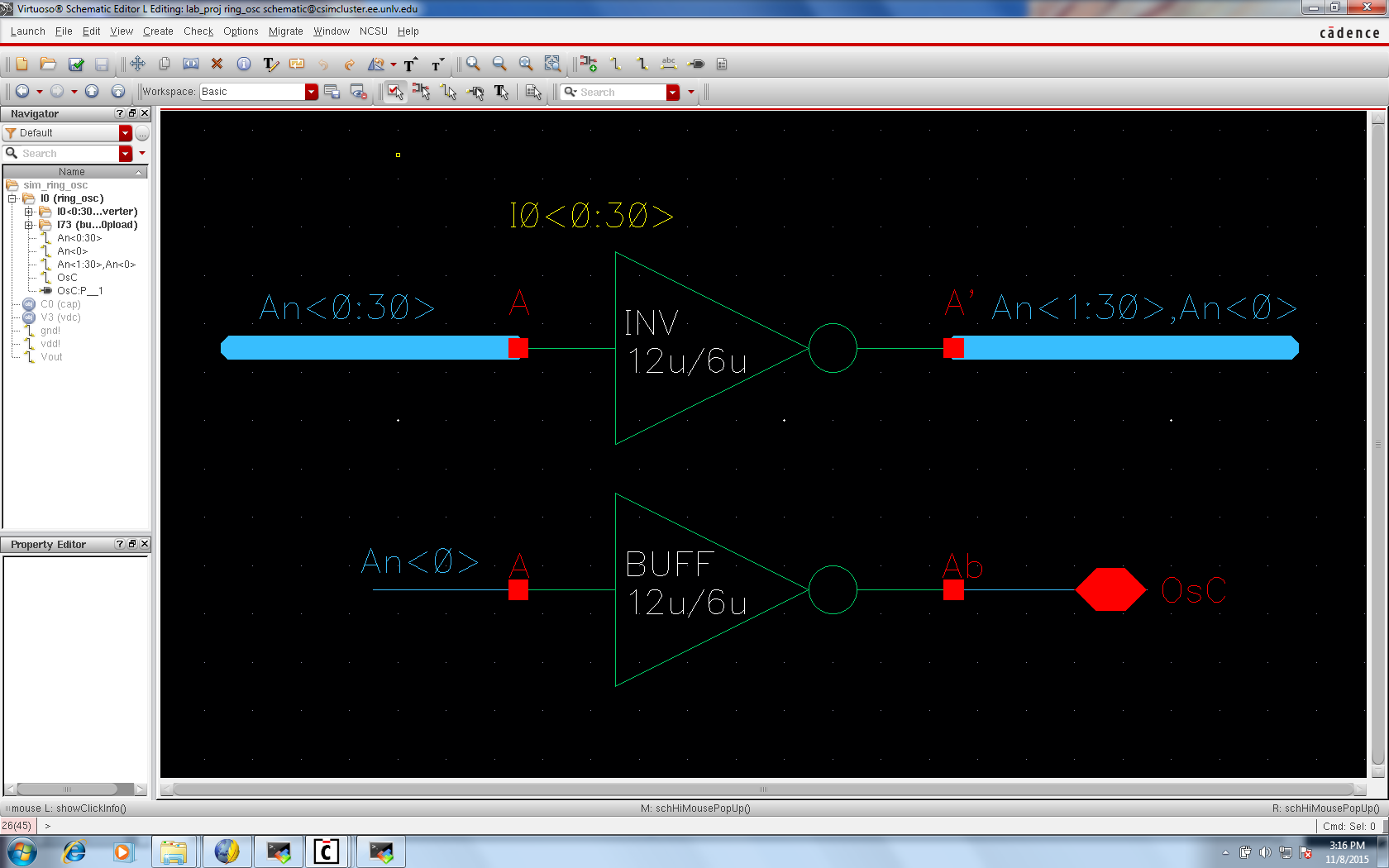
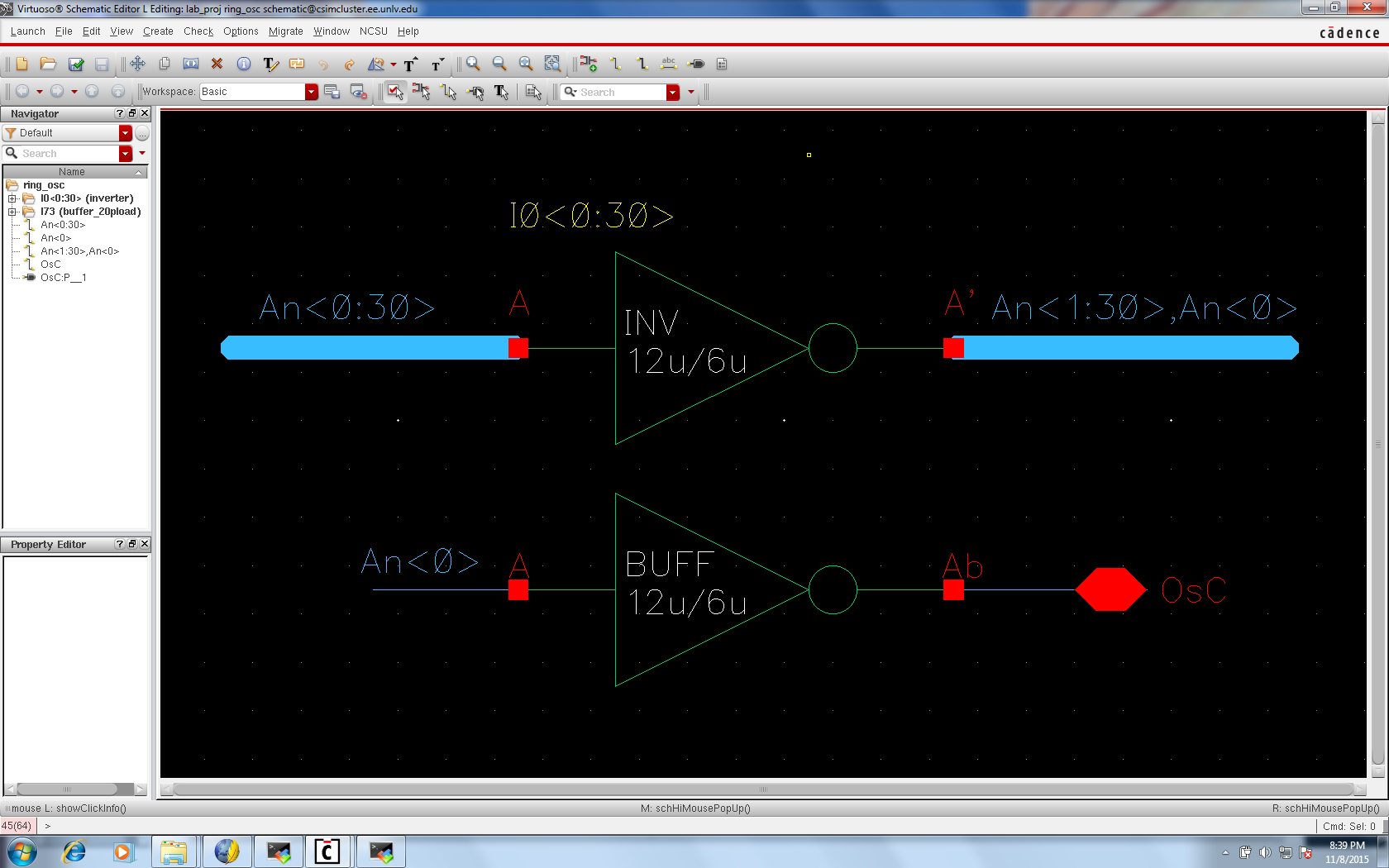
Oscillator Simulation Schematic
Refer
to miscellaneous section for buffer design.
Ring
Oscillator Simulation
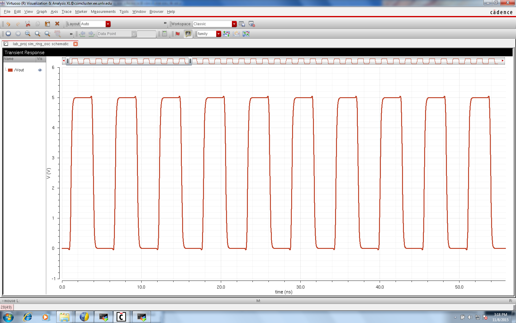
With the output buffered, a 20pf load may be connected to the oscillator while retaining the square waveform.
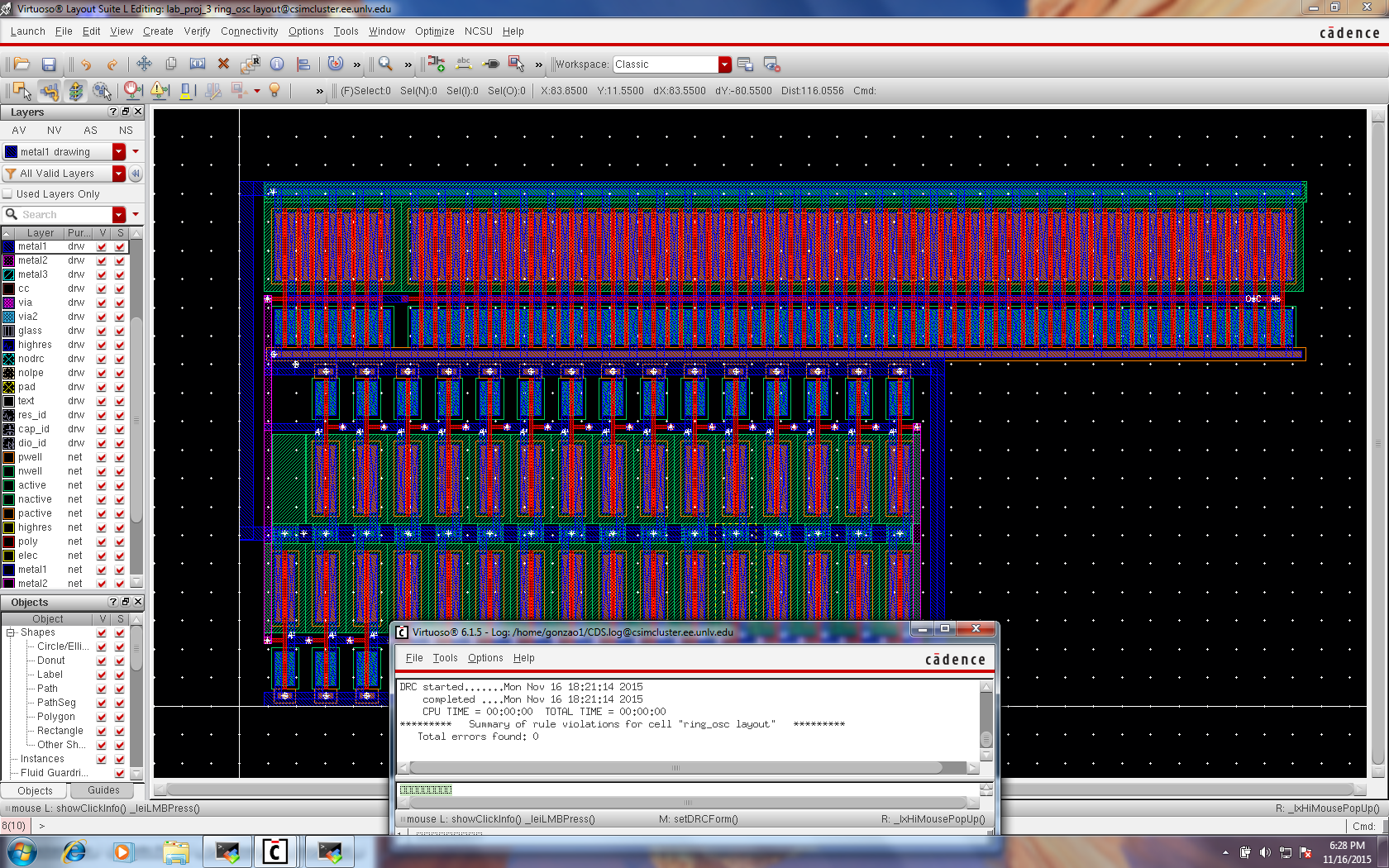
Ring Oscillator DRC
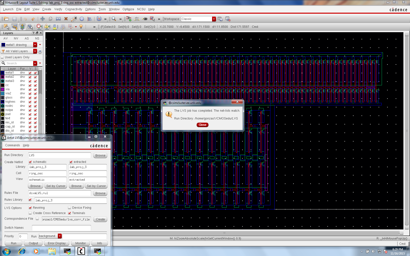
Ring Oscillator LVS
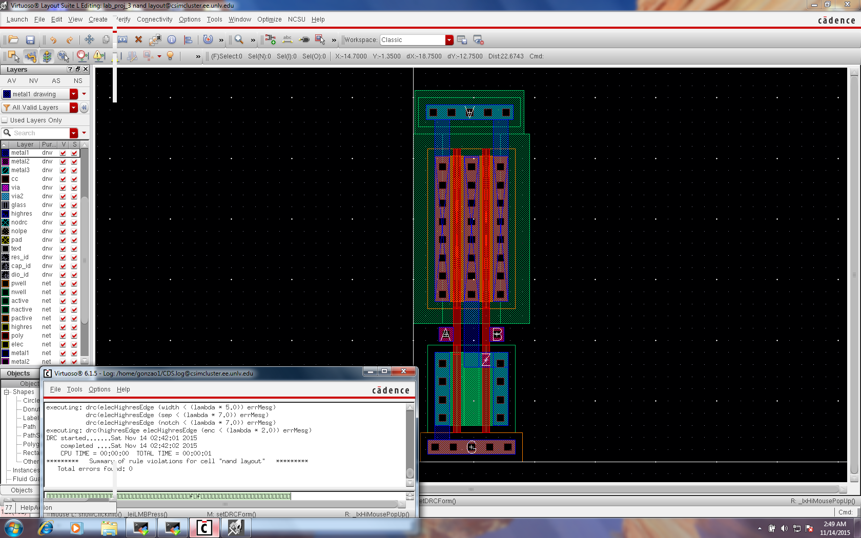
6u/0.6u NMOS/PMOS NAND and NOR Gates
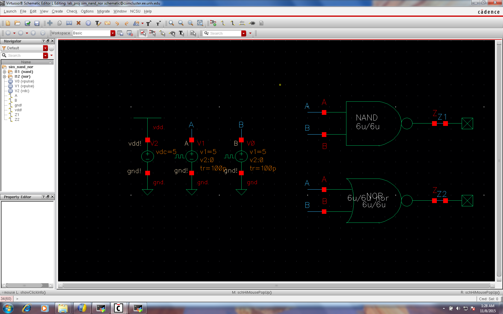
NAND and NOR Simulation Schematic
NAND and NOR Simulation
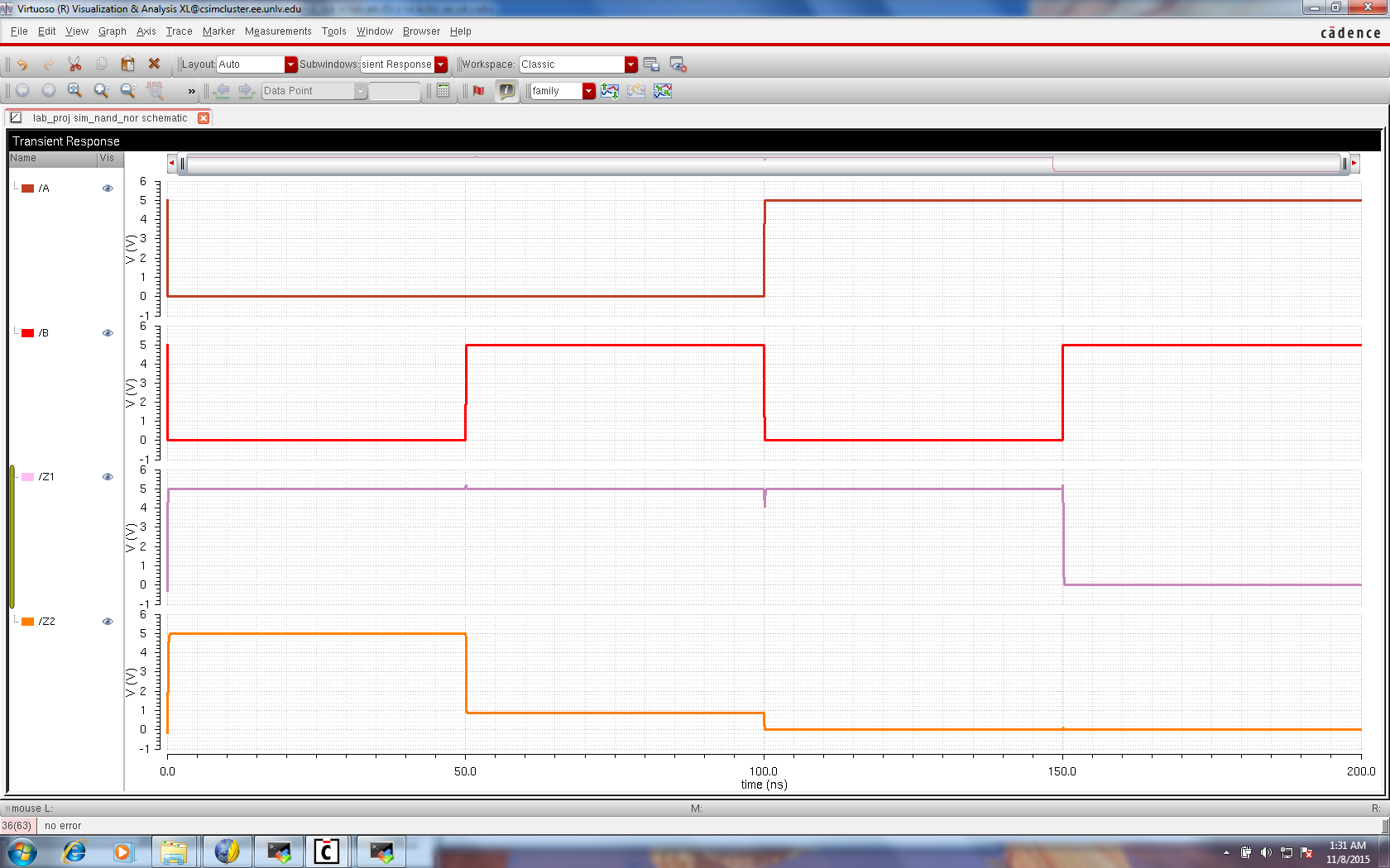
The simulation results for the mentioned gates are as expected based on the truth tables for the devices
NAND and NOR DRC
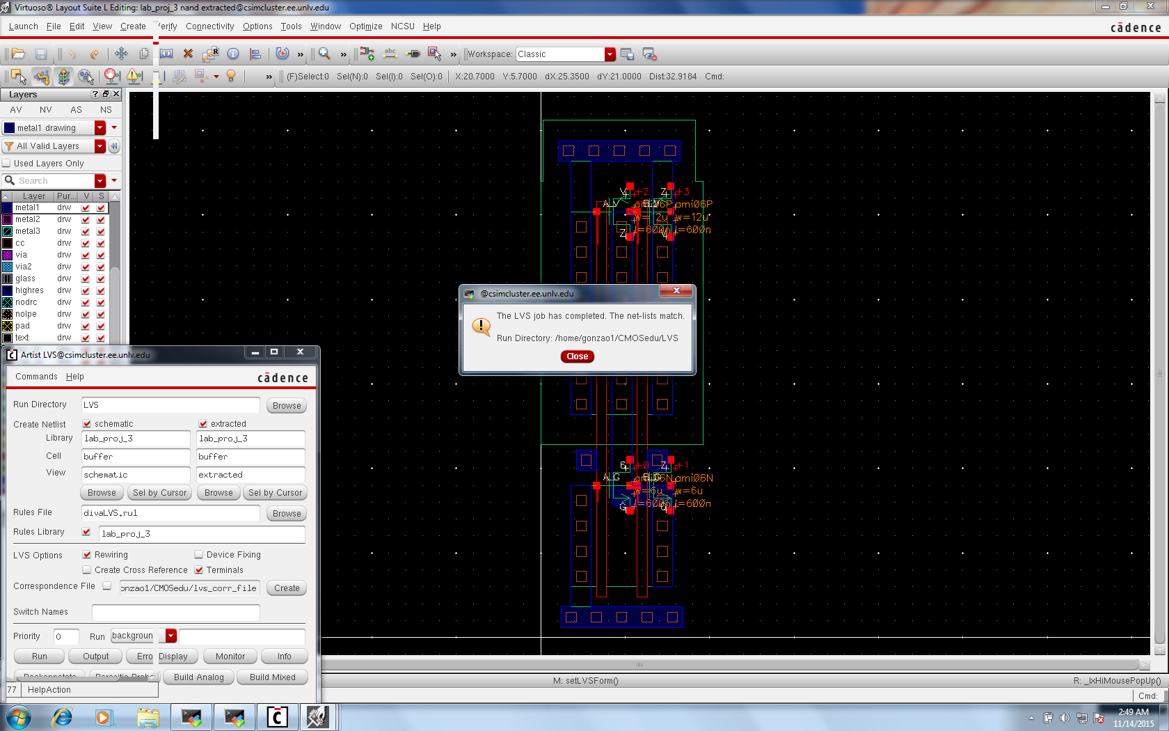
NAND
and NOR LVS
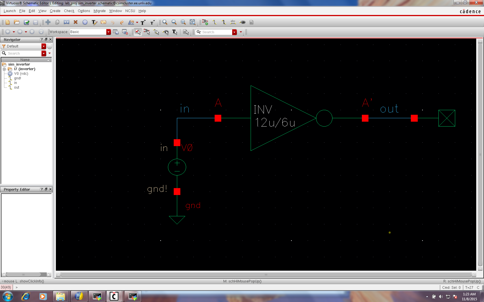
6u/0.6u NMOS/PMOS Inverter
Inverter Simulation Schematic
Inverter Simulation
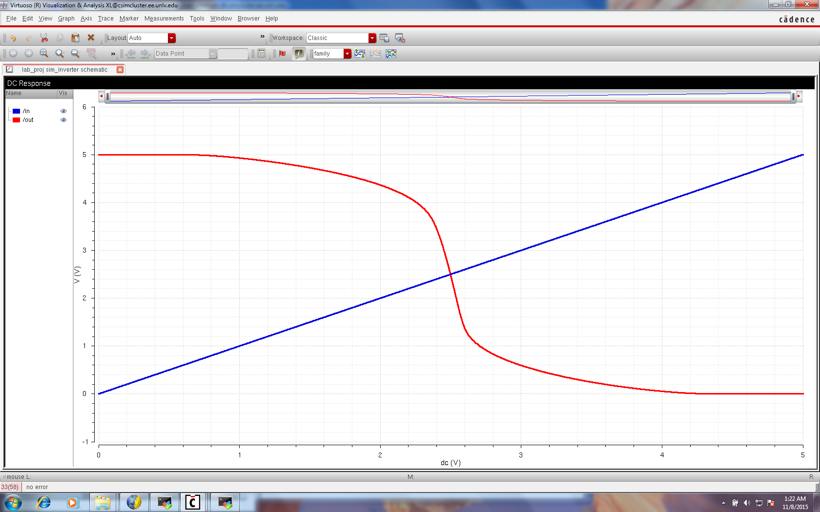
By sweeping the input to the gate the transfer curve above is generated, which agrees with a standard inverter profile.
Inverter DRC
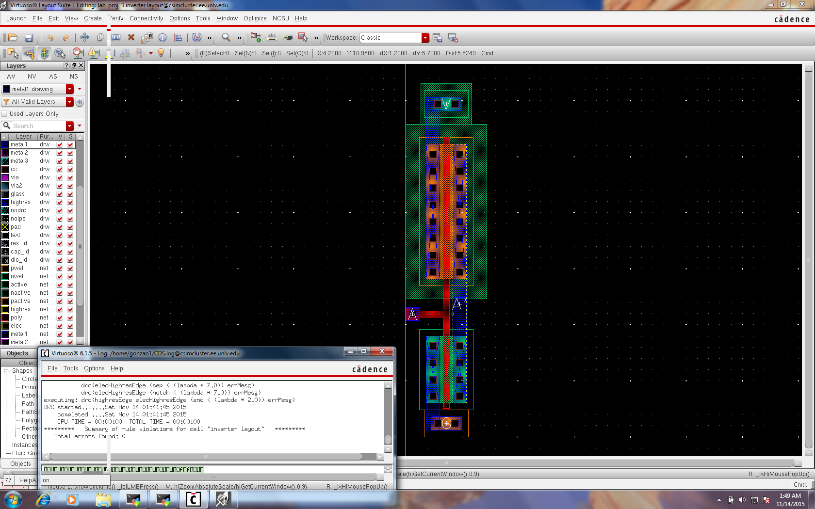
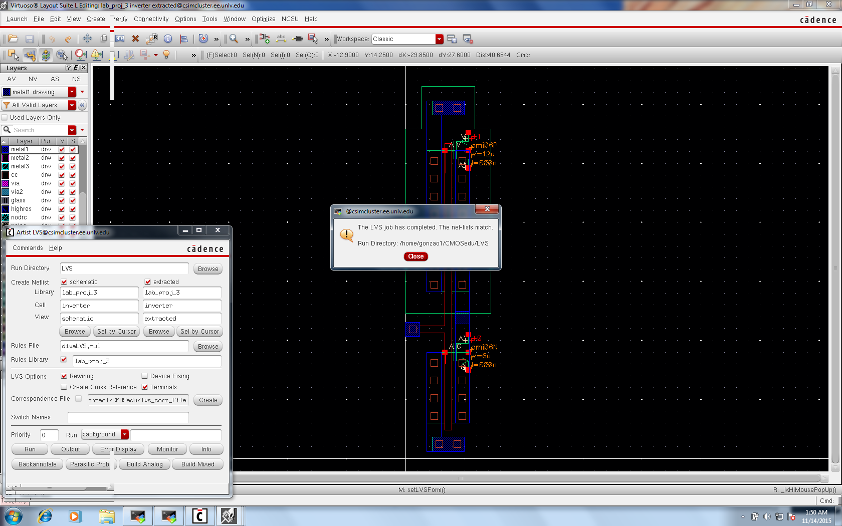
Inverter LVS
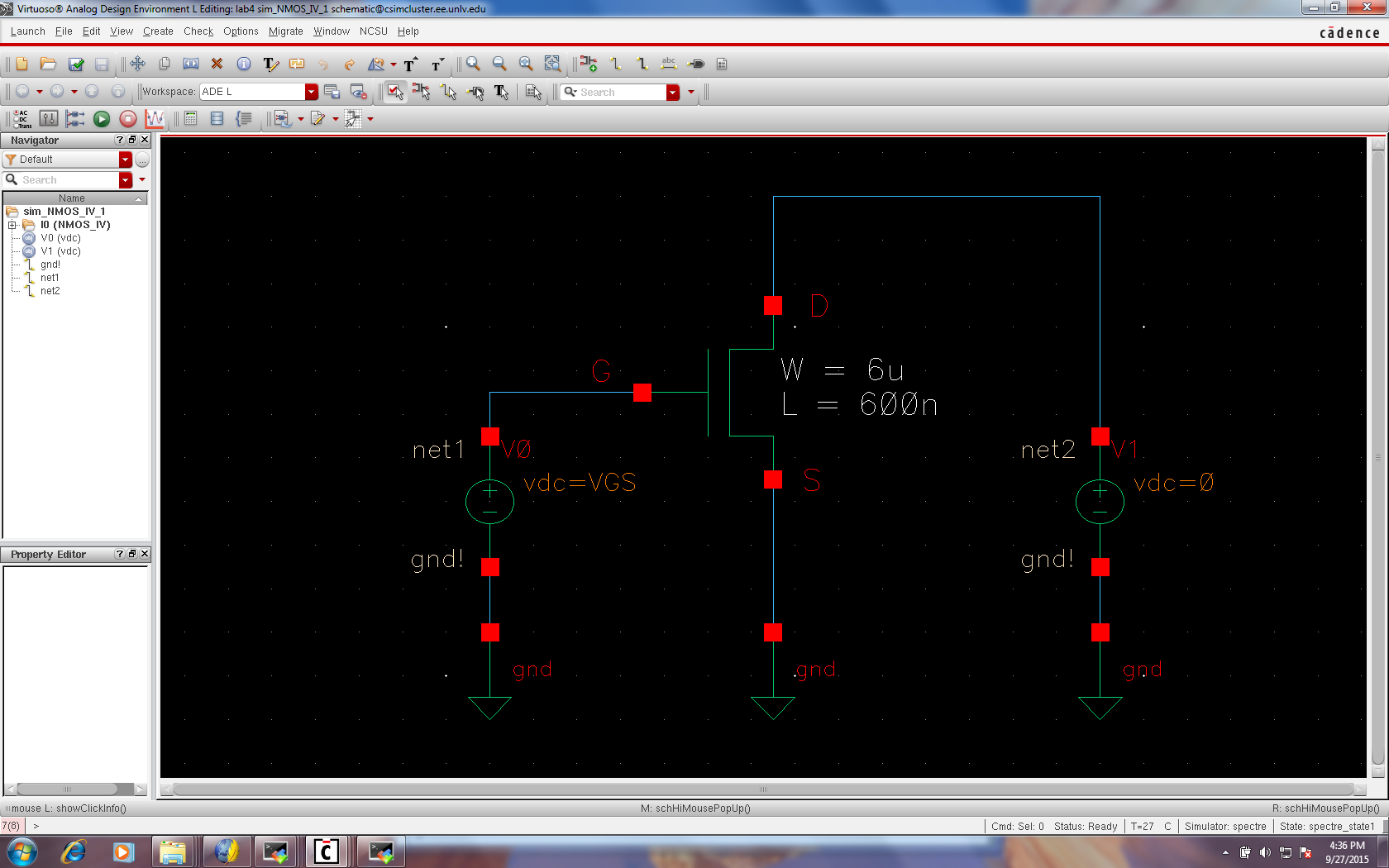
6u/0.6u NMOS and PMOS Transistors
NMOS
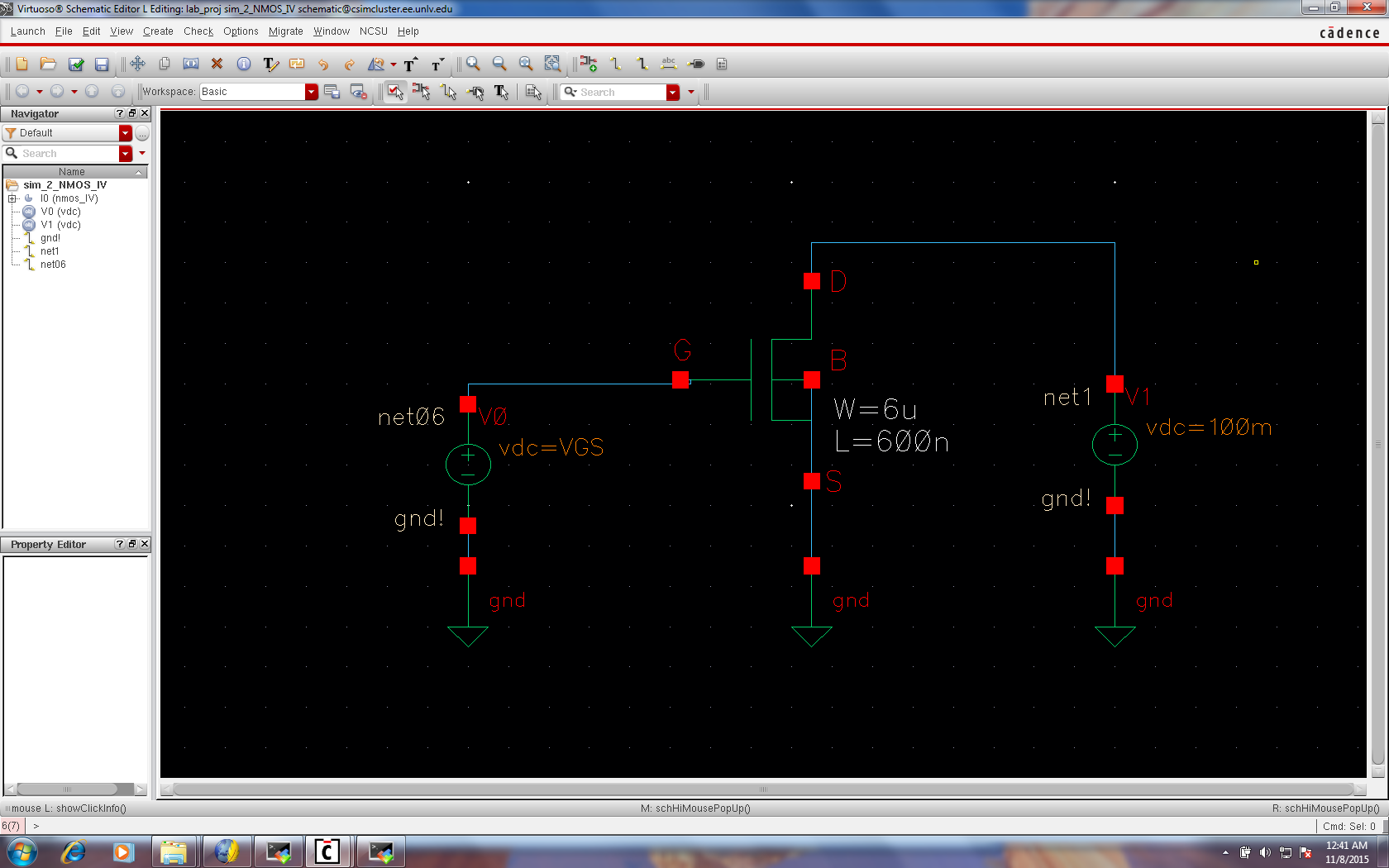
Transistor Simulation Schematic
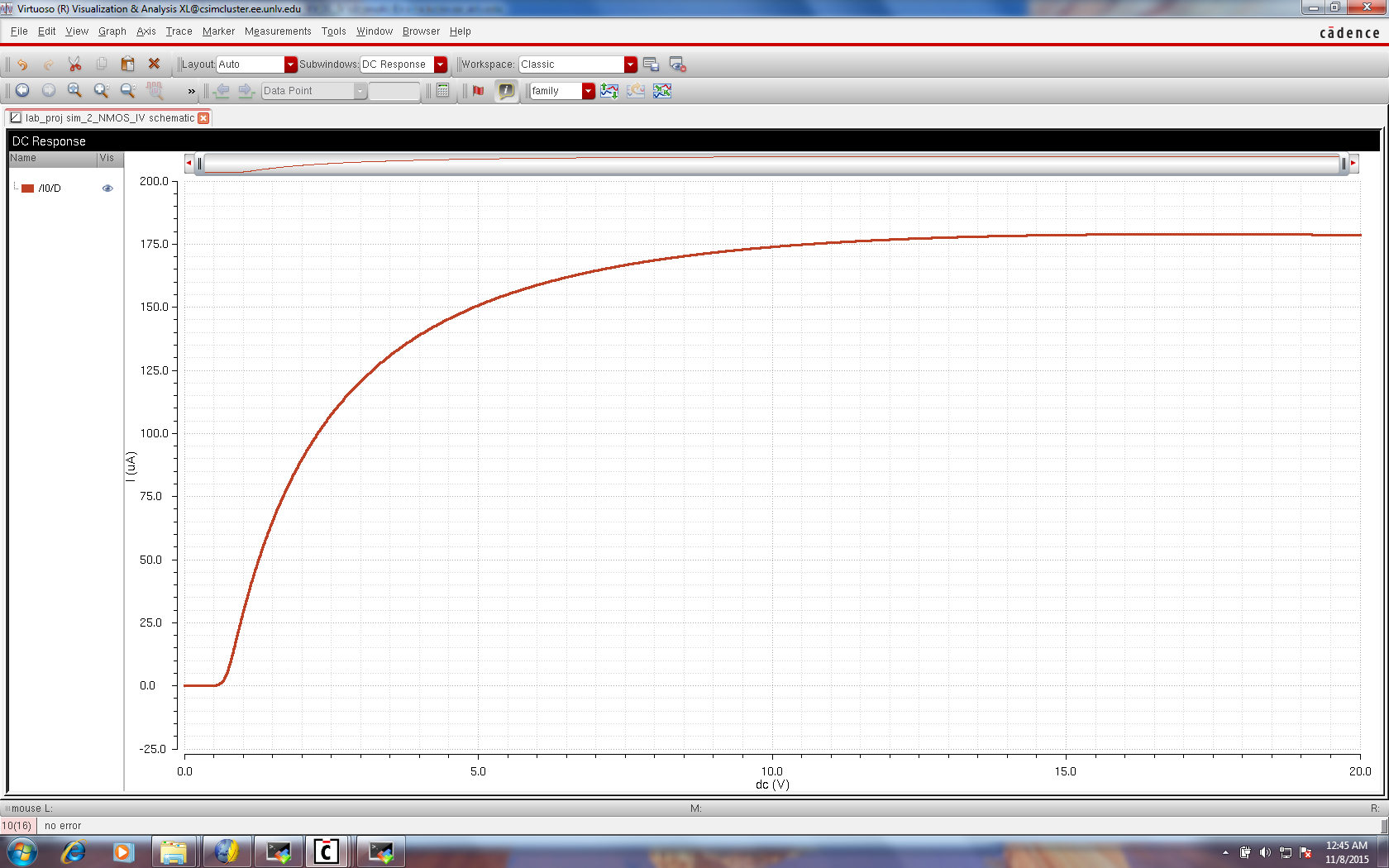
NMOS Transistor Simulation
NMOS
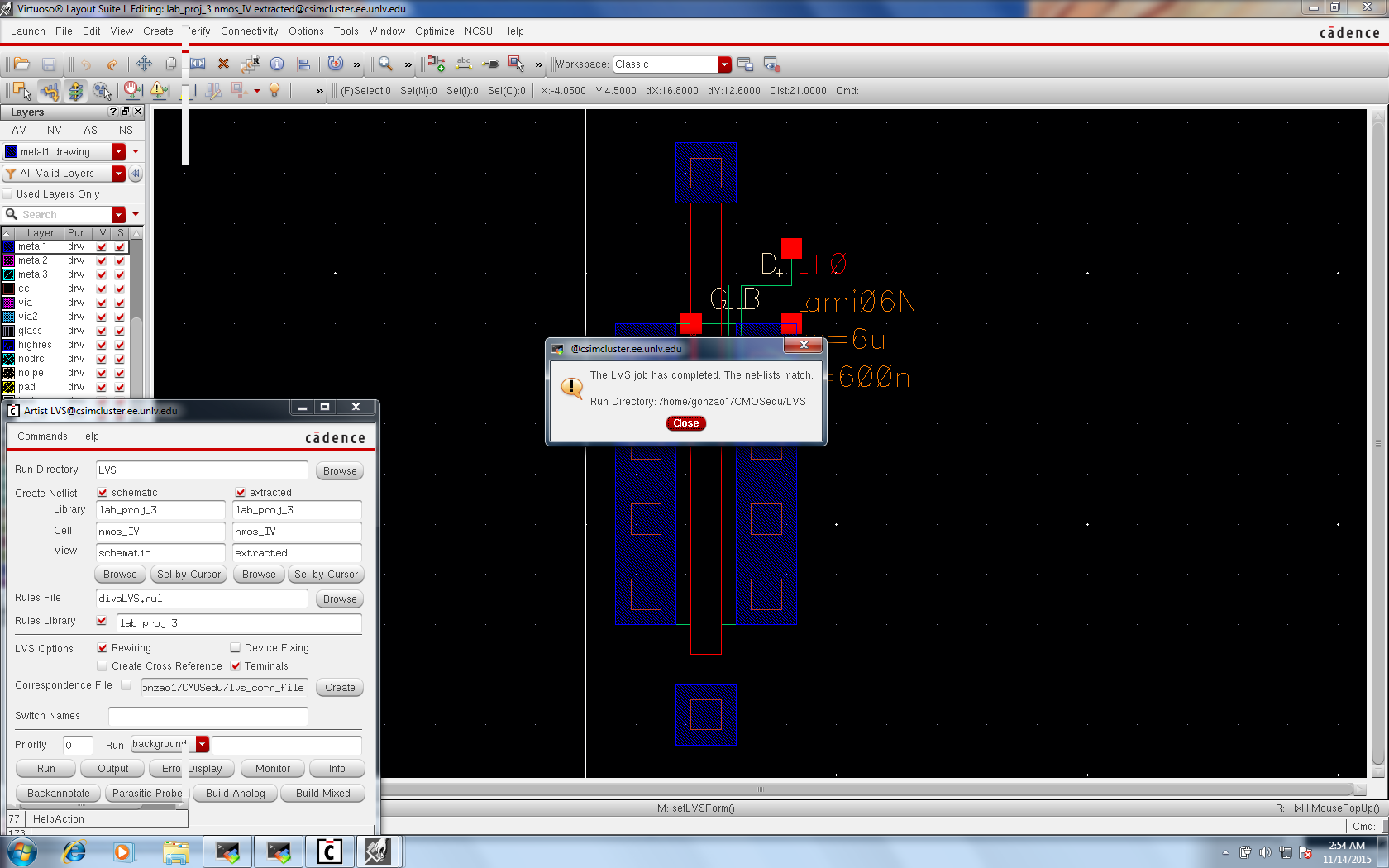
Transistor DRC
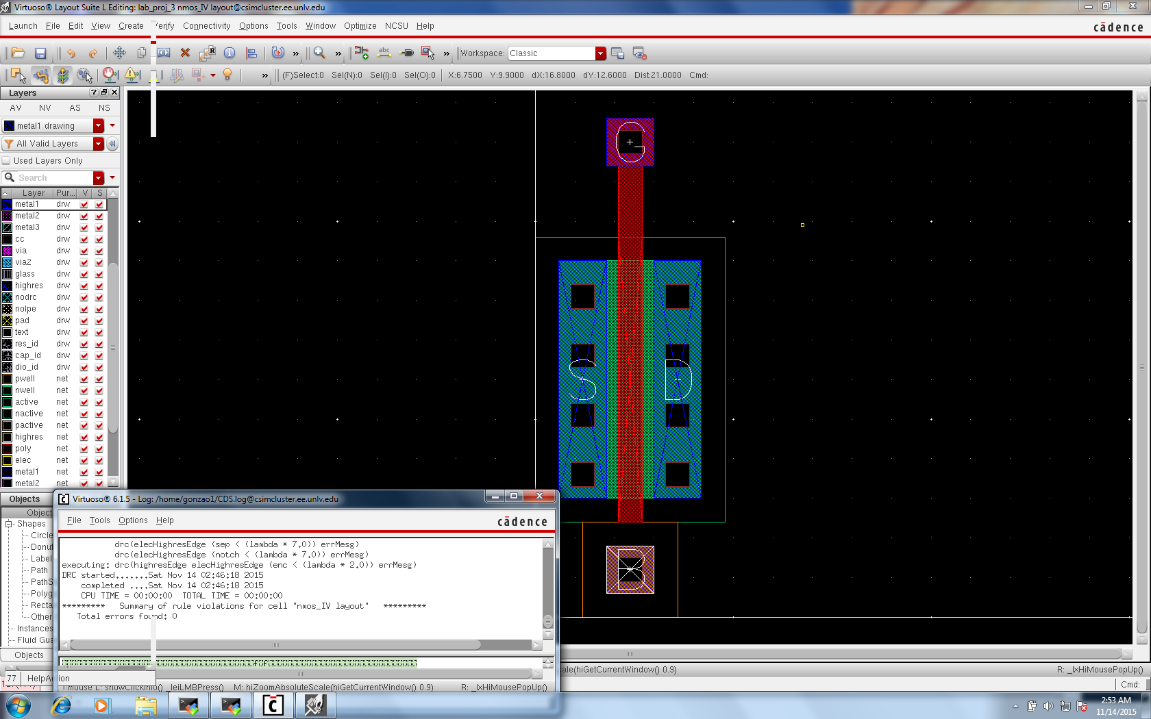
NMOS
Transistor LVS
PMOS Transistor Simulation Schematic
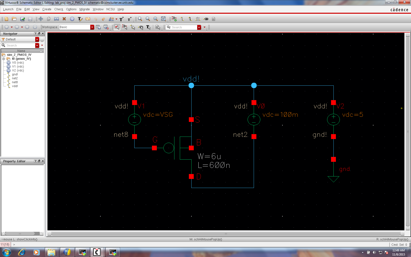
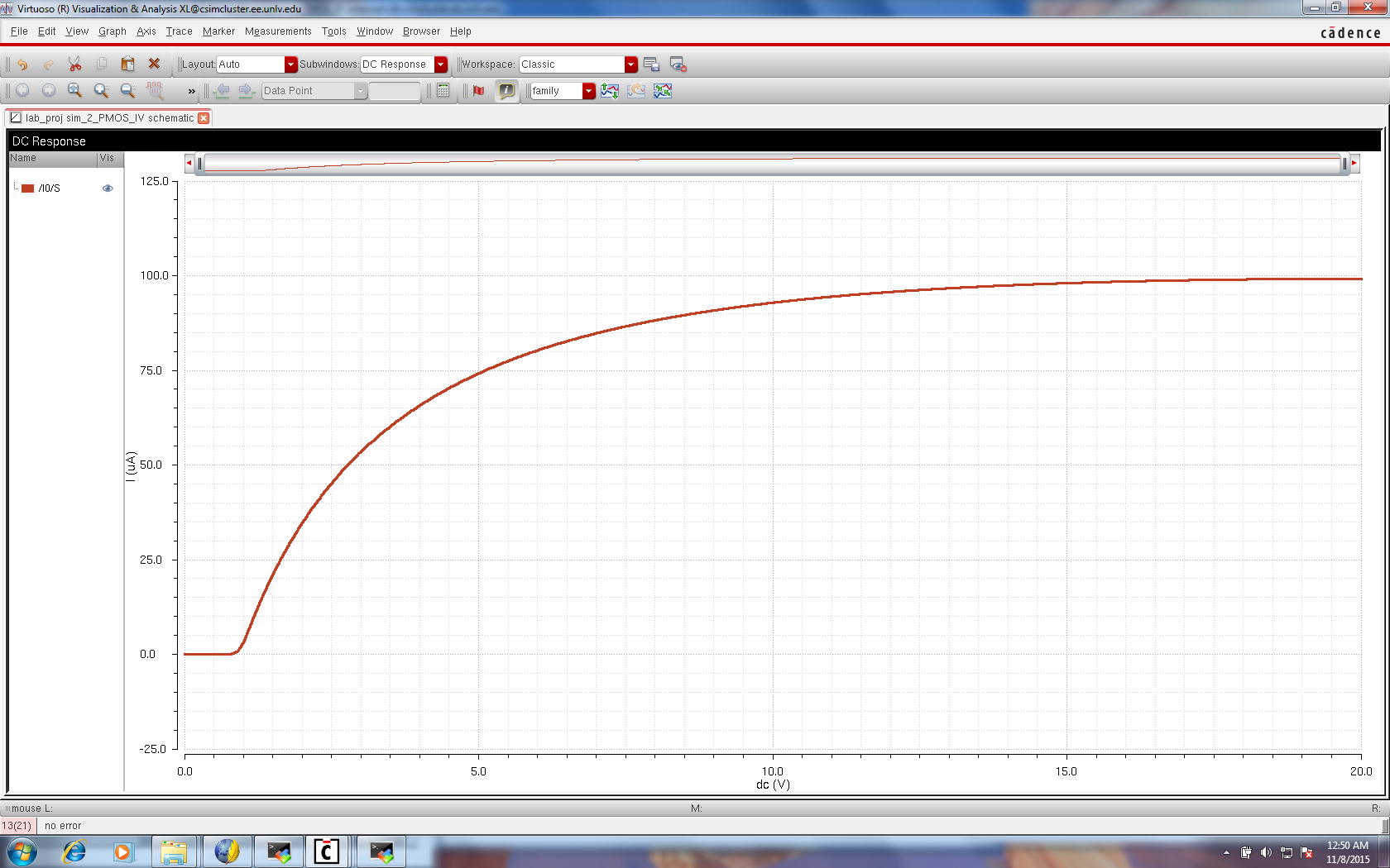
PMOS
Transistor Simulation
PMOS Transistor DRC
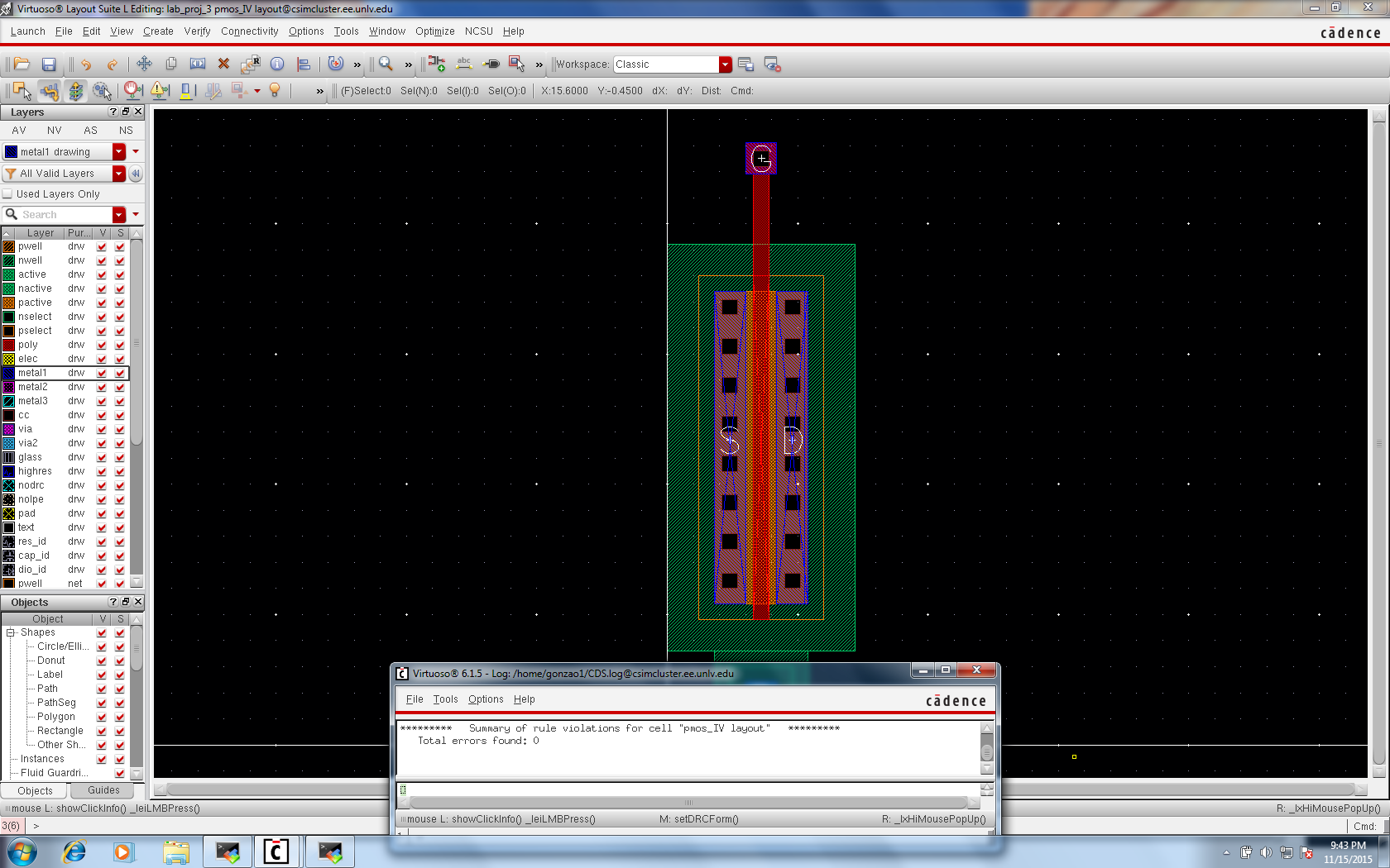
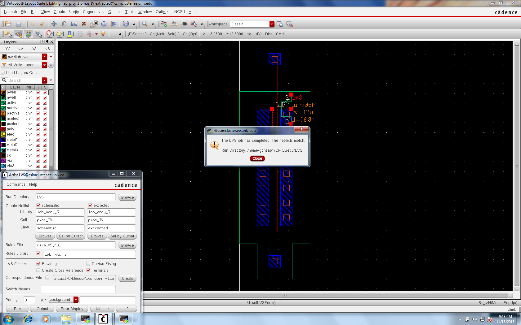
PMOS Transistor LVS
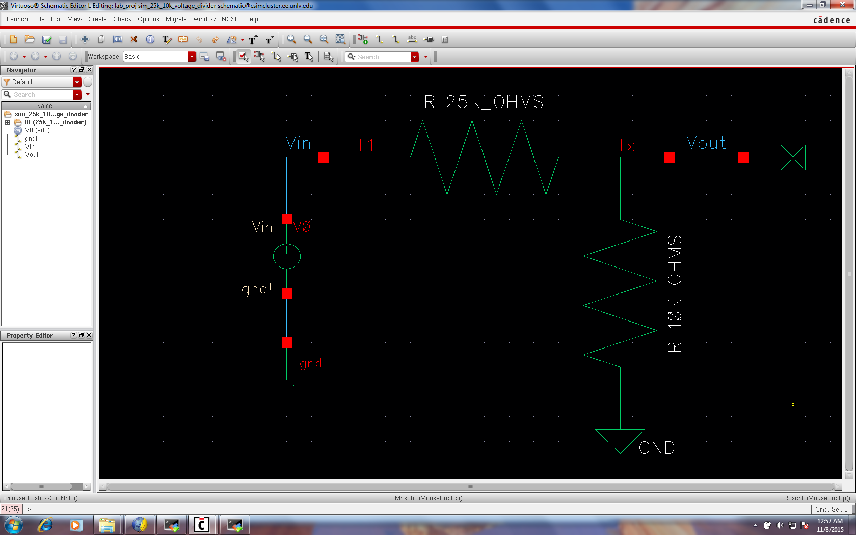
Voltage Divider - 25k/10k Resistors
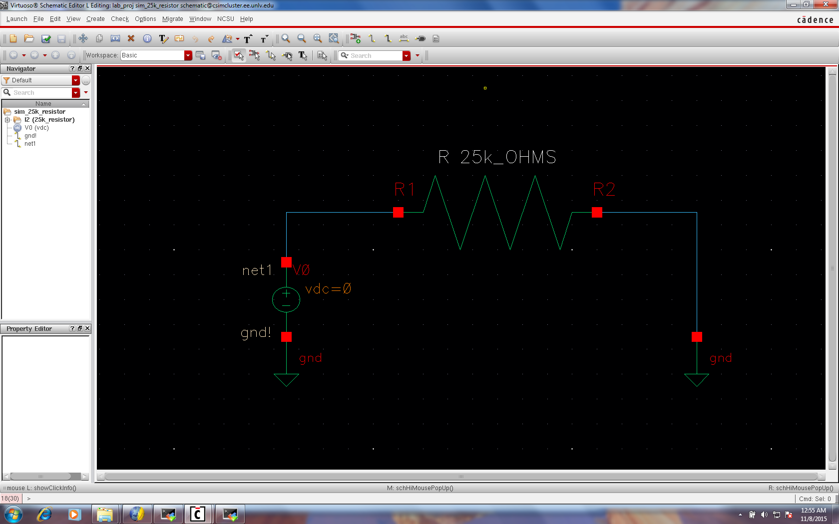
Voltage
Divider Simulation Schematic
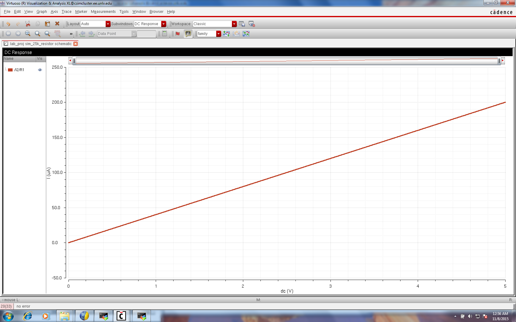
Voltage Divider Simulation
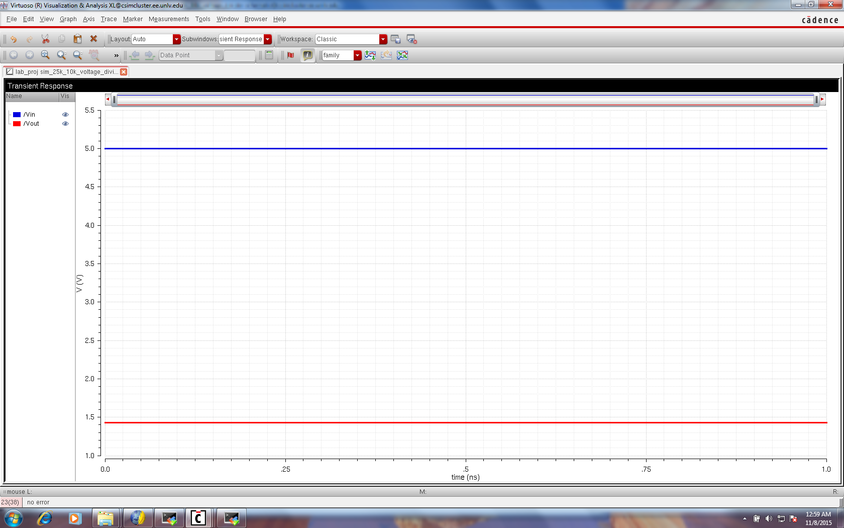
Recall from the voltage division principle the output voltage agrees with the simulation.
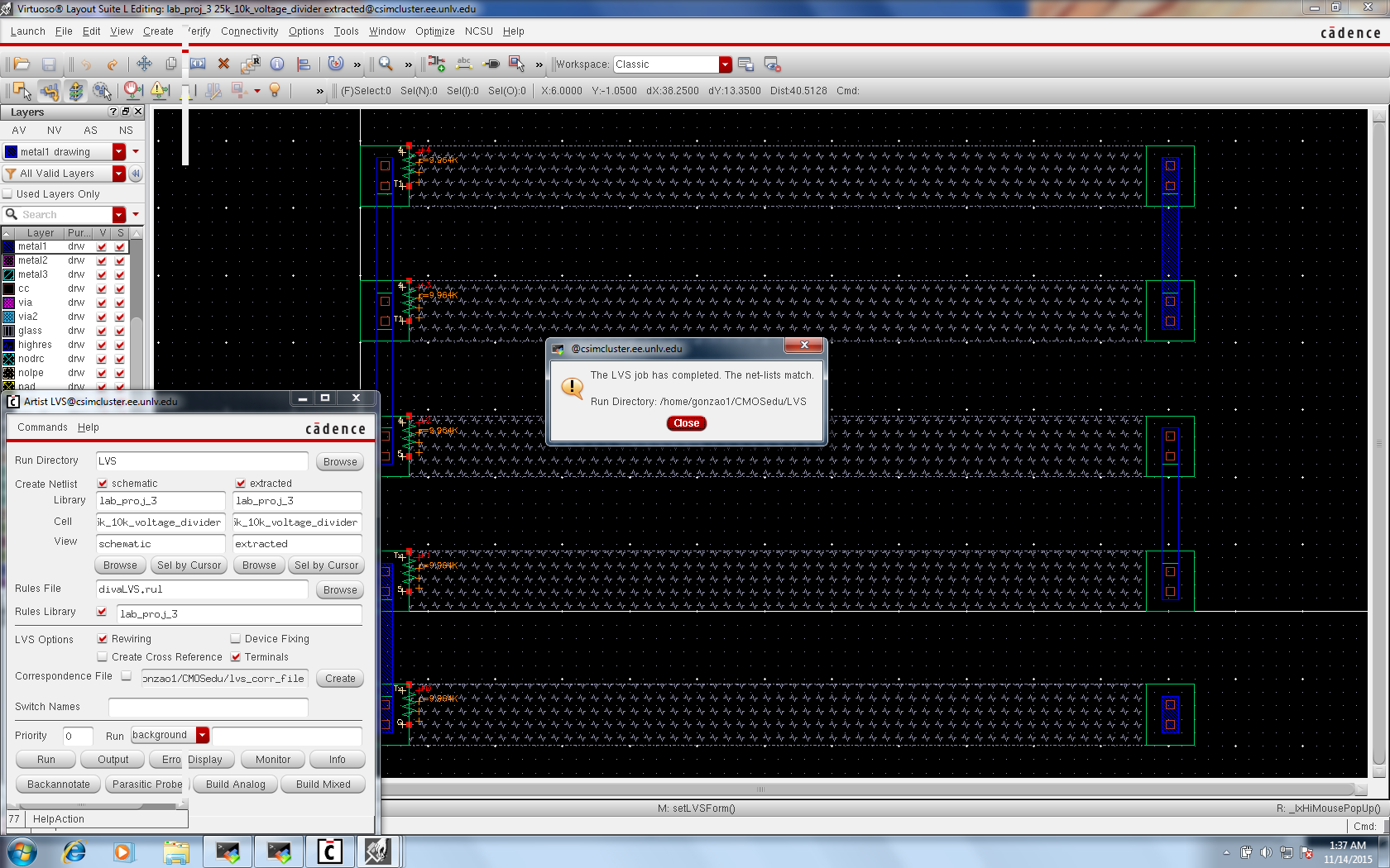
Voltage Divider DRC
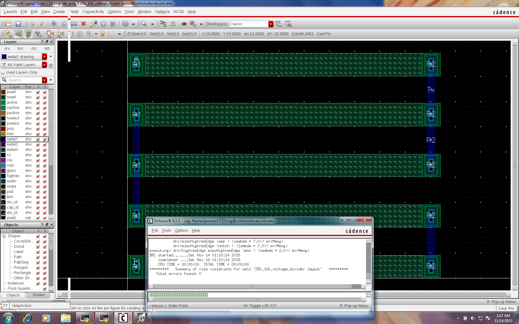
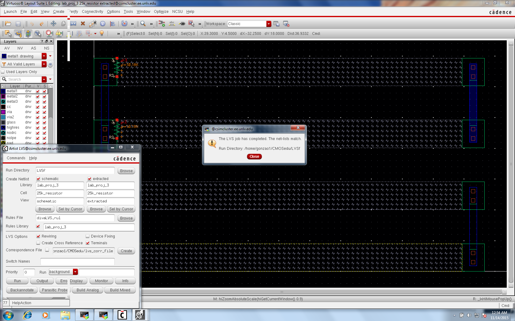
Voltage
Divider LVS
25k n-well Resistor
25k
Resistor Simulation Schematic
25k Resistor Simulation
Recall from Ohms Law, the slope of the curve is the resistance and correlates to 25k Ohms.
25k Resistor DRC
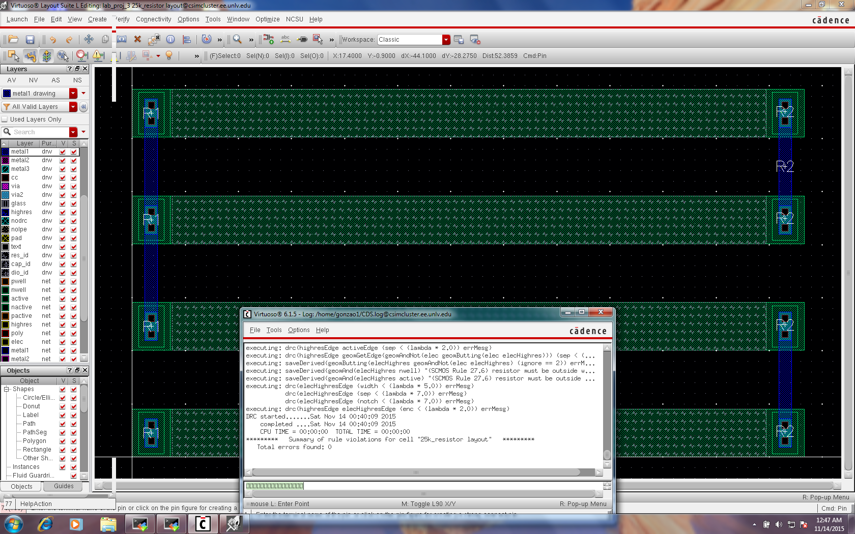
25k Resistor LVS
10k n-well Resistor
10k
Resistor Simulation Schematic
10k Resistor Simulation
Recall from Ohms Law, the slope of the curve is the resistance and correlates to 10k Ohms.
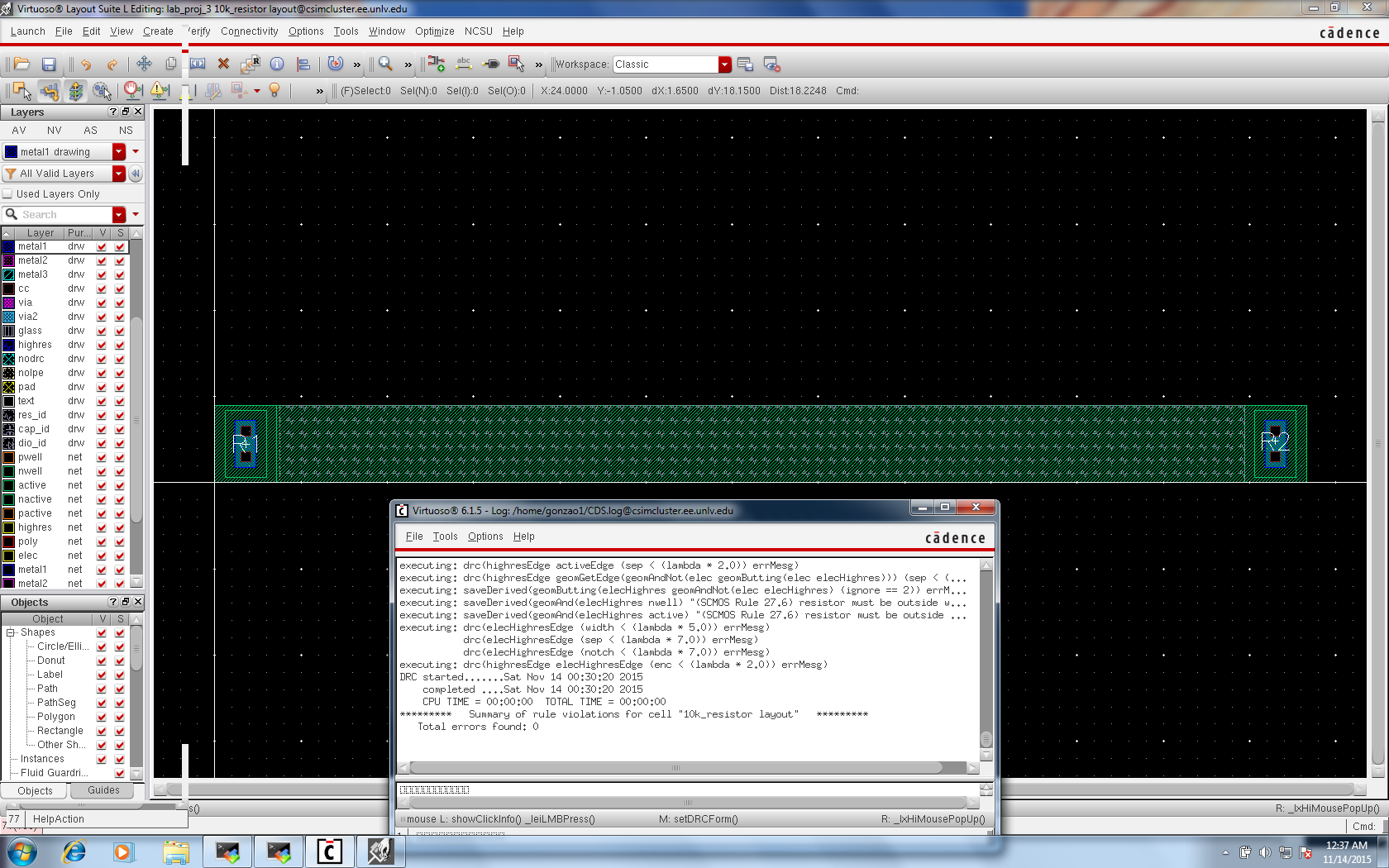
10k Resistor DRC
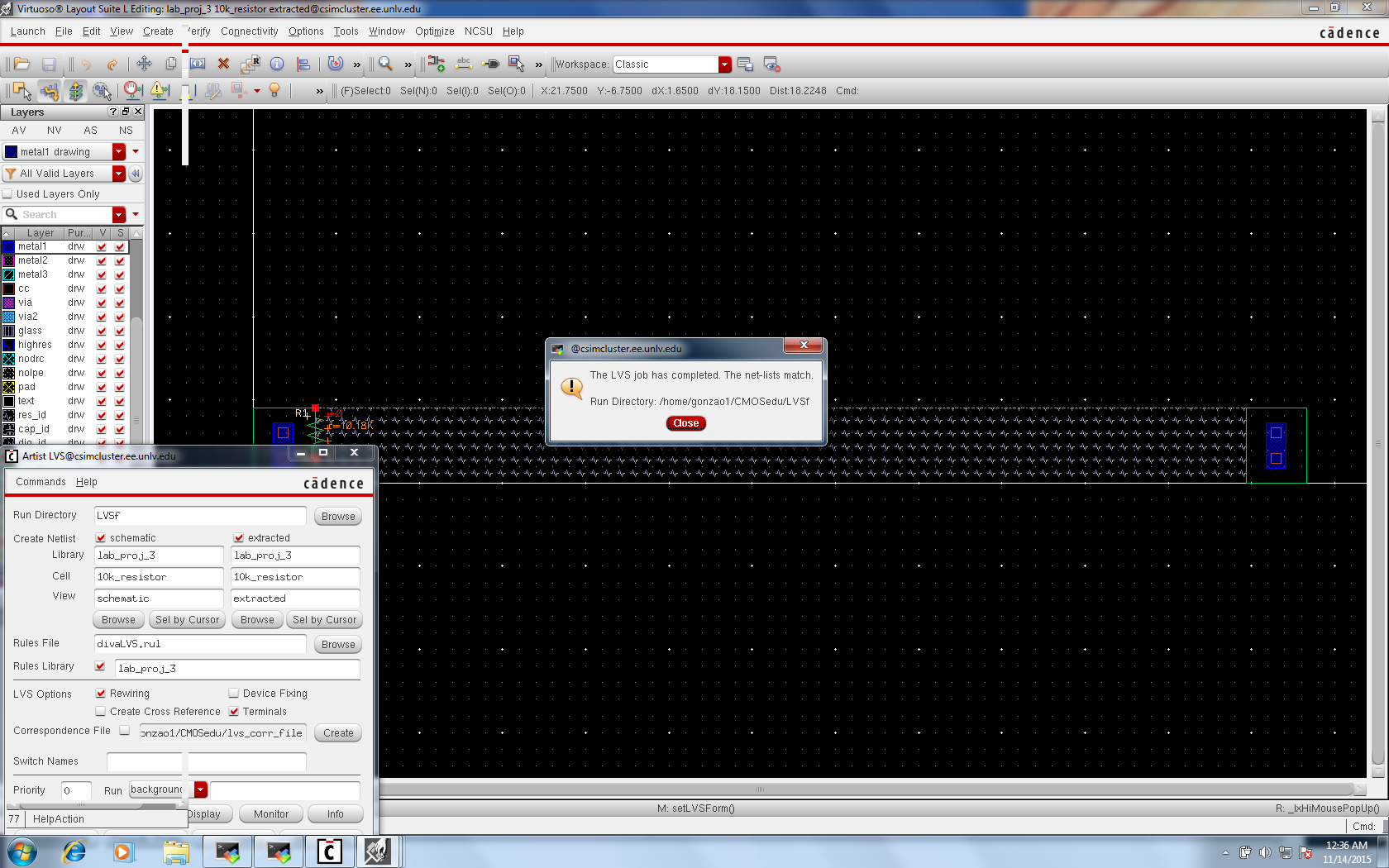
10k Resistor LVS
The
following devices were sub-level components used for the main test
structures.
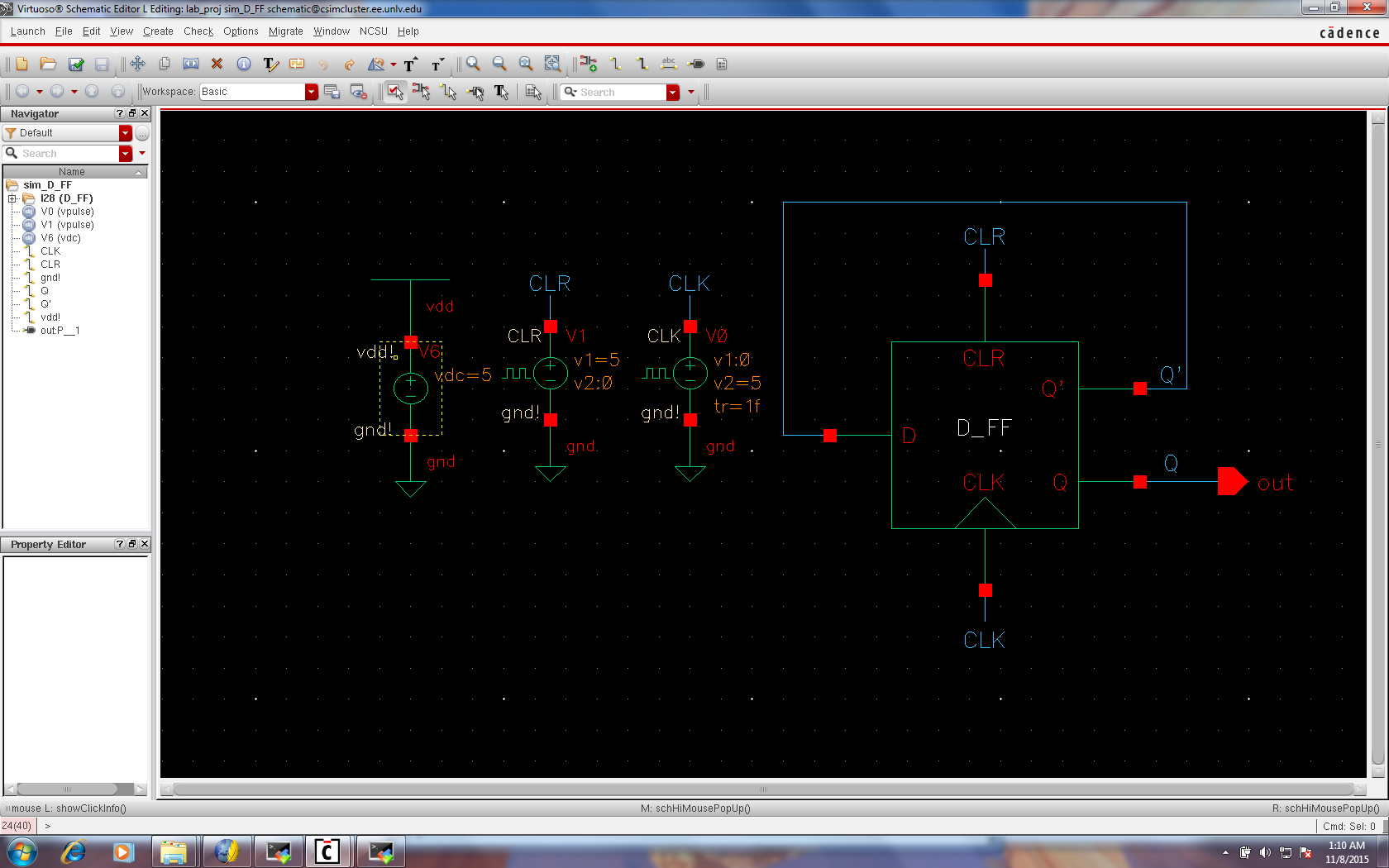
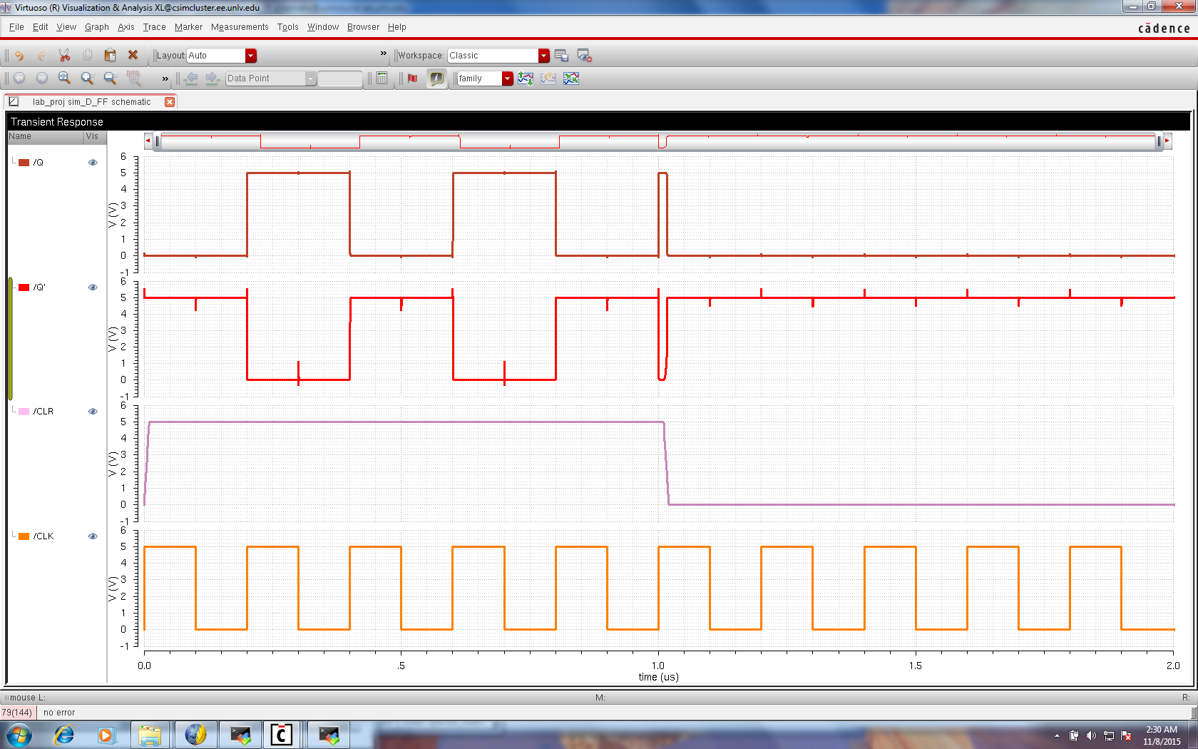
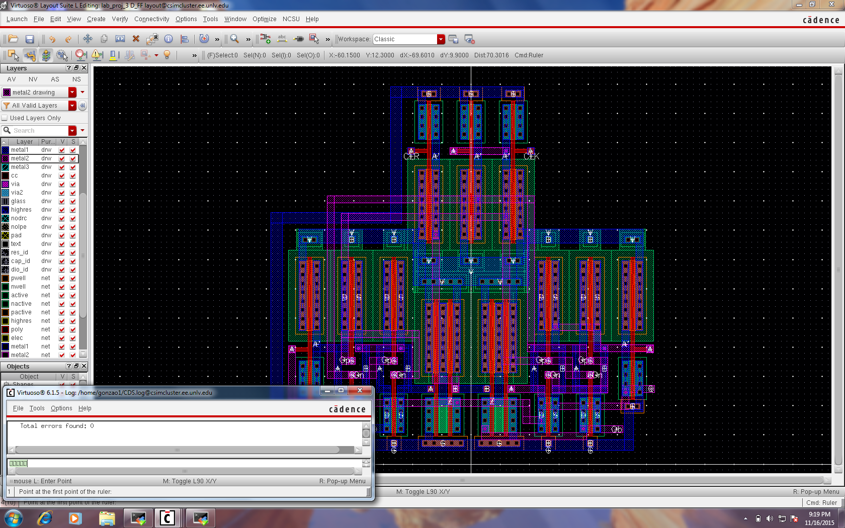
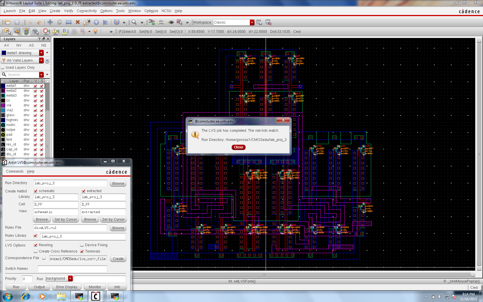
D Flip-Flop
D Flip-Flop Schematic
D Flip-Flop Simulation
D Flip-Flop DRC
D Flip-Flop LVS
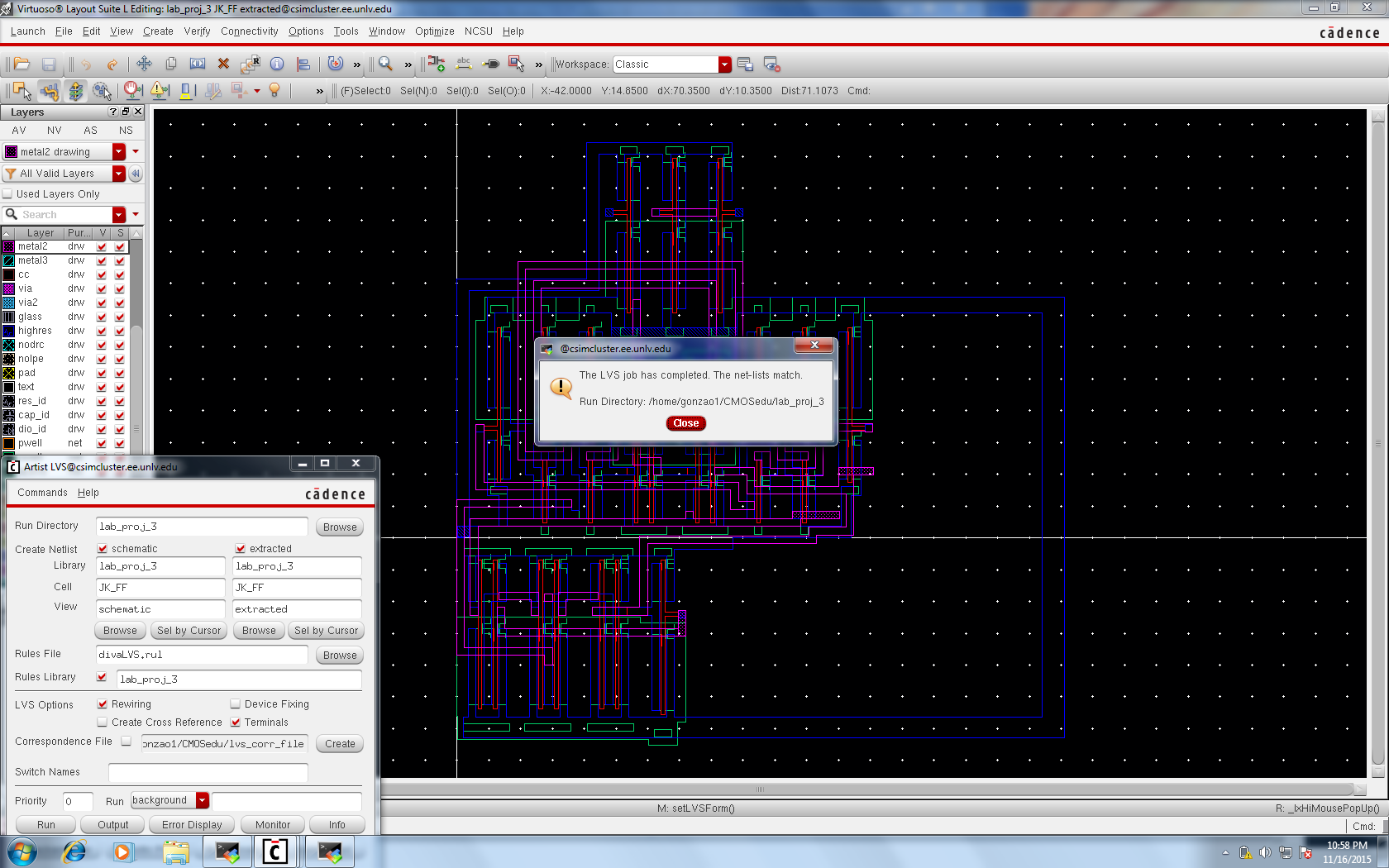
JK Flip-Flop
JK Flip-Flop DRC
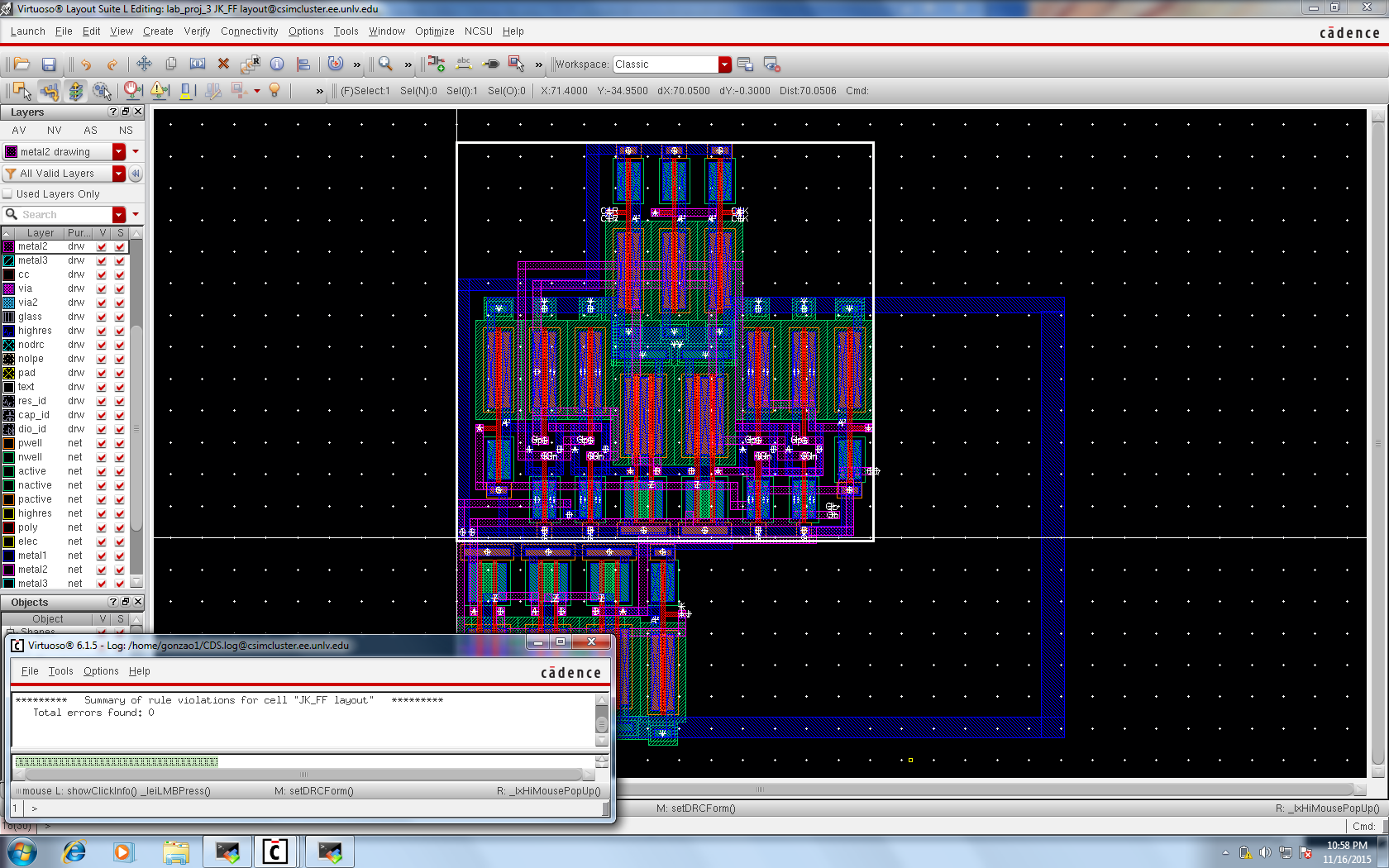
JK Flip-Flop LVS
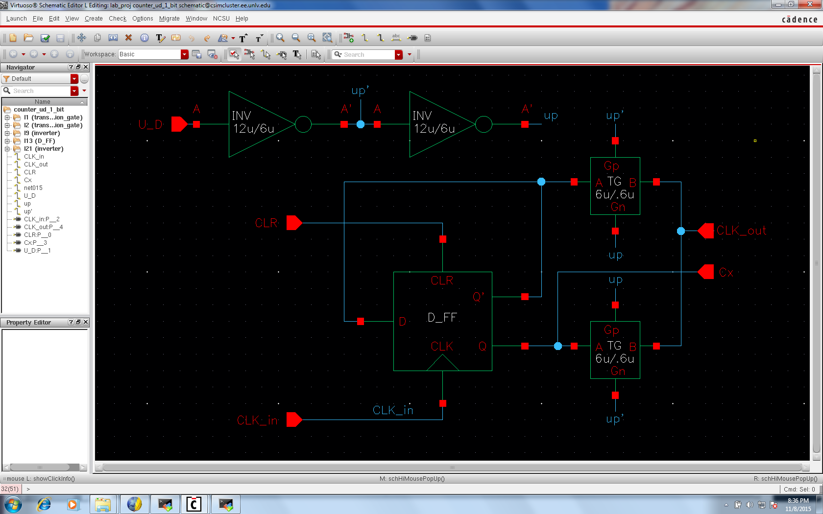
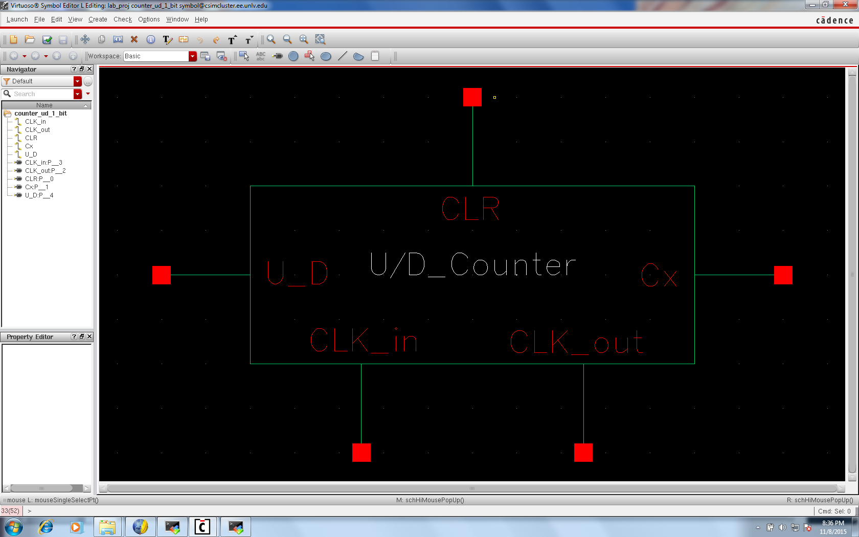
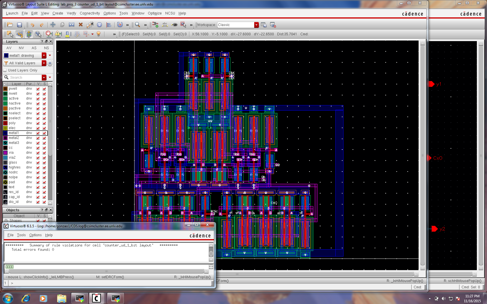
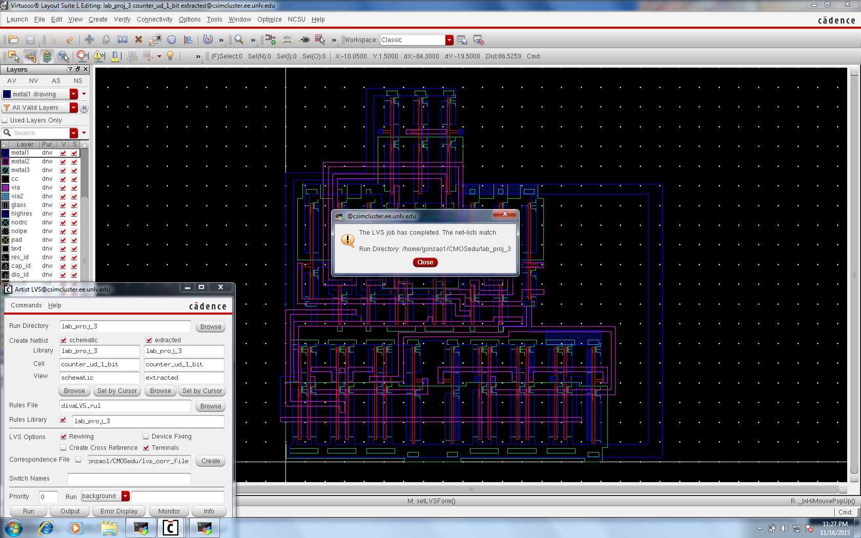
1-Bit Counter
1-Bit Counter Schematic
1-Bit Counter Symbol
1-Bit Counter DRC
1-Bit Counter LVS
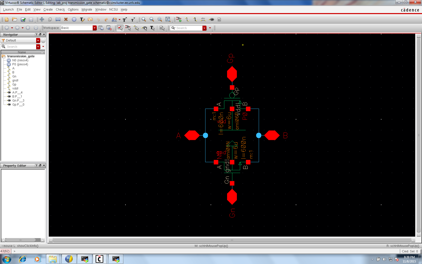
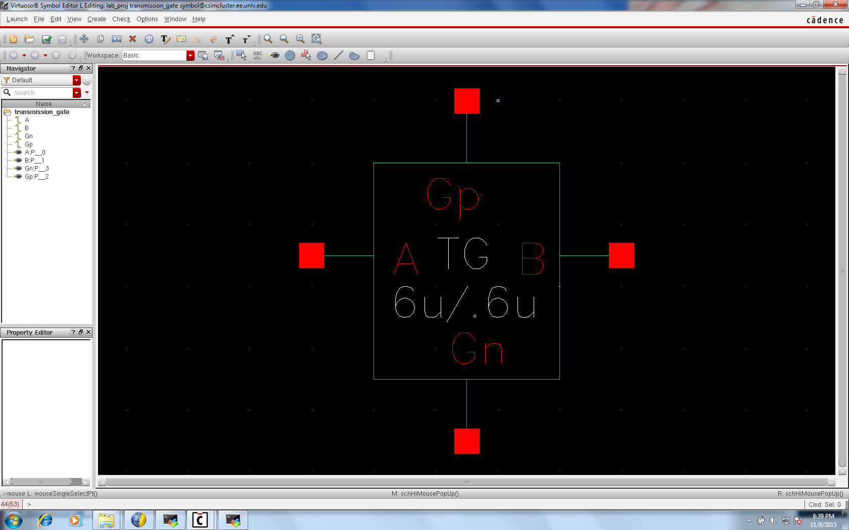
Transmission Gate
TG Schematic
TG Symbol
TG DRC
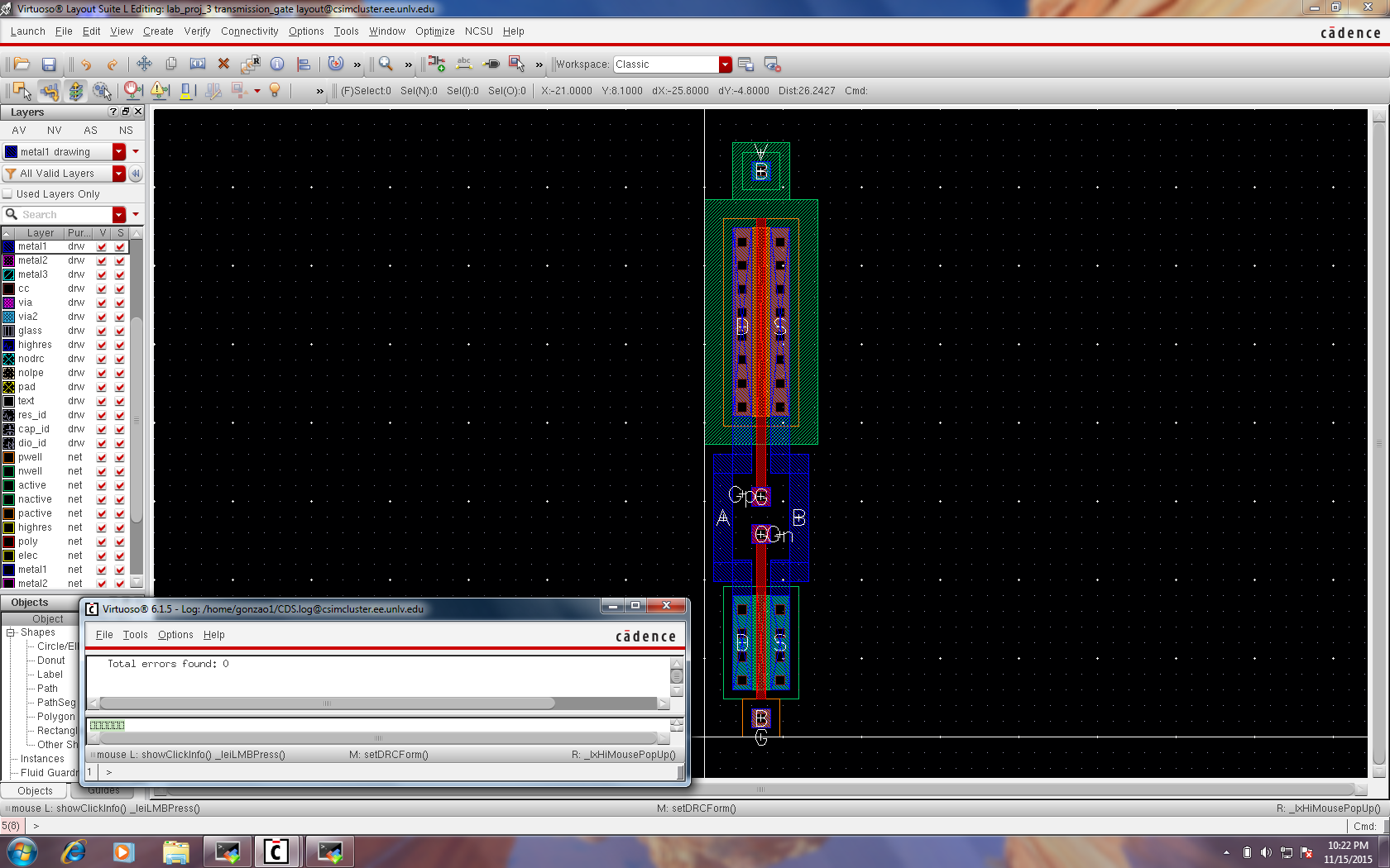
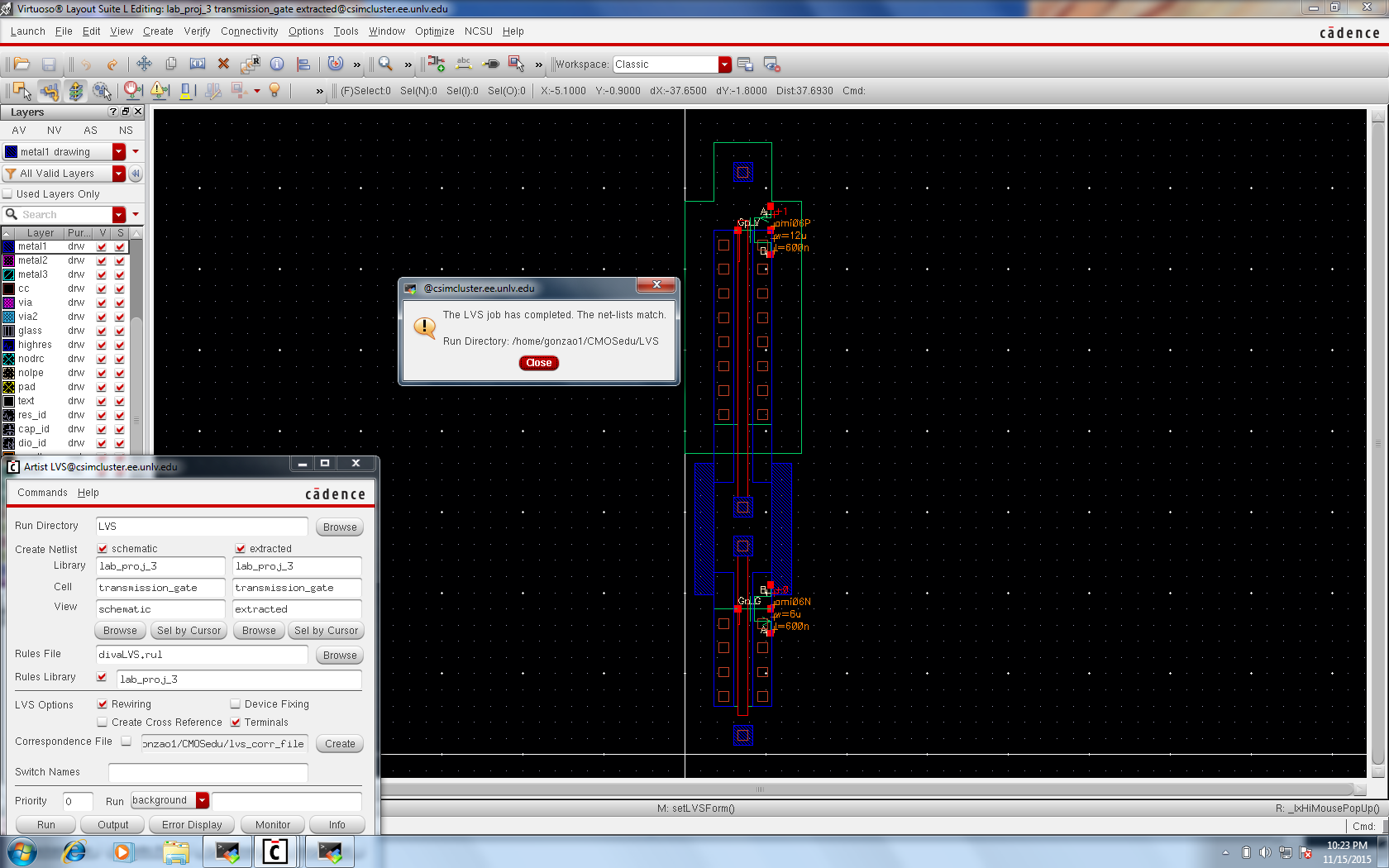
TG LVS
Ring Oscillator
Ring Oscillator Schematic
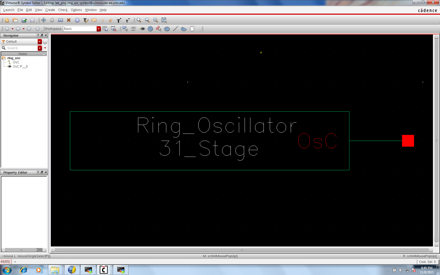
Ring Oscillator Symbol
Buffer
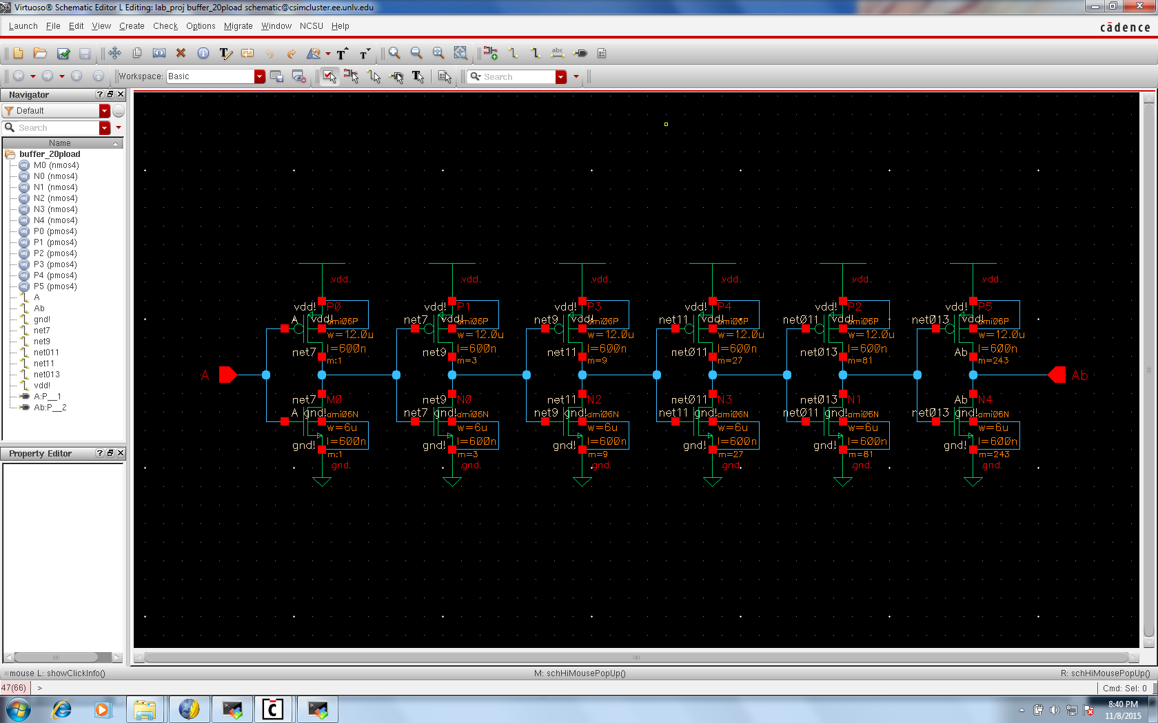
Buffer Schematic
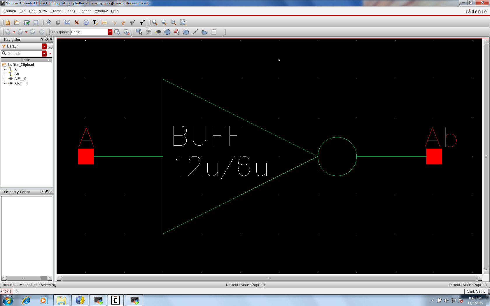
Buffer Symbol
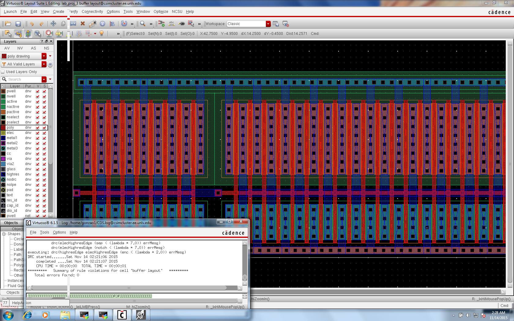
Buffer DRC
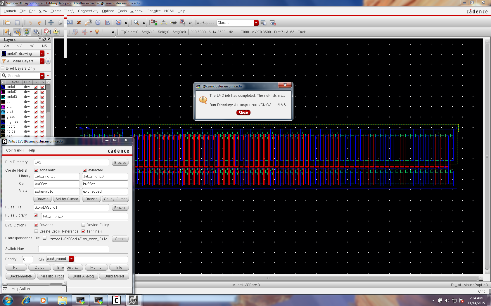
Buffer LVS
The
following is a link to the zipped chip design directory files for Lab 8
EE421 Lab 8 Design Directory.zip
The webpage and design directory was backed-up during the pre-lab portion of the lab.
Lab 8 served as a means to generating a test chip layout for submission to MOSIS for fabrication using the ON's C5 process.